Design of a High Step-Up Interleaved Boost
Converter with PI controller
Anwishta Saha
1, Goutam Kumar Panda
2Pradip Kumar Saha
3PG Student [Power Electronics and Drives], Dept. of EE, Jalpaiguri Govt. Engineering [Autonomous] College, Jalpaiguri, India.1
Professor & HOD, Dept. of EE, Jalpaiguri Govt. Engineering [Autonomous] College, Jalpaiguri, India.2 Professor, Dept. of EE, Jalpaiguri Govt. Engineering [Autonomous] College, Jalpaiguri, India.3
ABSTRACT: Generally conventional boost converters have been used to obtain higher output voltage than the input voltage. When these boost converters are operated for high ratios it leads to high voltage and current stress on the switch. Hence an interleaving technique of boost converter has been presented. This method of approach can be used in high power applications to produce high voltage gain when compared to the conventional boost converter. This project report deals with the simulation of Interleaved Boost Converter (ILBC). It is seen that, for higher power applications, more modules can be paralleled to increase the power rating and the dynamic performance. One of the challenges in designing a boost converter for high power application is how to handle the high current at the input side. In this project report an interleaved boost dc-dc converter is proposed for current sharing on high power application. Moreover, this converter also reduces the ripple of voltage. The simulated results are presented with R load.
KEYWORDS:Boost converter, Closed loop control, Interleaved, PI controller, Ripple factors.
I.INTRODUCTION
Power converters have required improvement as well as reduction of size and weight especially in mobile information/communication devices, traction converters, power control units for electric/hybrid vehicle, etc. Passive components and cooling devices usually occupy a much larger space than semiconductor devices in power electronics building block. It is well known that when many DGs are connected to utility grids, they can cause problems such as voltage rise and protection problem in the utility grid. To solve these problems, new concepts of electric power systems are proposed [1]. Resonant converters eliminate most of the switching losses encountered in Pulse Width Modulation converters. The active device is switched with either Zero Current Switching or Zero Voltage Switching at its terminals. When current through the switch is made zero, it is turned on /off, it is known as zero current switching and when voltage across the switch is made zero, it is turned on / off, it is known as zero voltage switching [2]. The main objective of this project report is to develop a modular high-efficiency high step-up boost converter with a forward energy-delivering circuit integrated voltage-doubler as an interface for high power applications. In the proposed topology, the inherent energy self-resetting capability of auxiliary transformer can be achieved without any resetting winding. Moreover, advantages of the proposed converter module such as low switcher voltage stress, lower duty ratio, and higher voltage transfer ratio features are obtained [3].
ISSN (Print) : 2320 – 3765 ISSN (Online): 2278 – 8875
I
nternational
J
ournal of
A
dvanced
R
esearch in
E
lectrical,
E
lectronics and
I
nstrumentation
E
ngineering
(An ISO 3297: 2007 Certified Organization) Vol. 4, Issue 2, February 2015
input current can be shared among the phases, which is desirable for energy dissipation [7]. The features of the interleaved boost dc-dc converter, the principle of operation and the design procedure are discussed in this project report. The simulation and experimental results are presented.
II.INTERLEAVED BOOST CONVERTER
In case of boost converter ripple is present in the input current due to rise and fall of inductor current. This problem can be eliminated by using interleaved boost converter .This technique consists of a phase shifting of the control signals of cells in parallel operating at the same switching frequency. The main advantage are the current distribution .The current in the switches are just a function of the input current .So interleaved boost converters can reduce input current ripple and the switching losses.
III.ILBC OPERATING PRINCIPLE
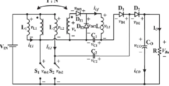
The proposed interleaved converter topology with high voltage transfer ratio is proposed as shown in Fig.1. The proposed converter consists of two-phase circuits with interleaved operation. The first phase is a boost integrating the forward-type circuit structure, which includes inductor L1 and switch S1 for the boost and an isolated forward energy-delivering circuit with turn ratio N. The second phase of the proposed converter is a boost circuit which contains inductor L2, switch S2, blocking capacitor C2, and diode D2 followed by the common output capacitor Co. From Figure.1, one can see that the proposed converter is basically based on the conventional voltage-doubler for the second phase circuit. However, for the first phase, in order to reduce the voltage stress of switch S1 and diode D1, an additional blocking capacitor C1, is added to function as that of C2 for the second phase. The operation principle can be described by considering the key waveforms of the proposed converter as shown in Figure.2. For simplicity, assume that all the components in Figure.1 including the high-frequency transformer of the forward energy delivering circuit are assumed ideal and under steady-state condition.
Figure.2: Key waveforms of the proposed converter.
IV.MODES OF OPERATION
Mode 1 [t0 < t ≤ t1]:From Fig. 2, one can see that for mode 1, switches S1, S2 are turned on. Diode Df1 is forward biased, while diodes D1,D2,Df2 are reverse biased. During this operation mode, both iL1 and iL2 are increasing to store energy in L1 and L2, respectively. Meanwhile, the input power is delivered to the secondary side through the isolation transformer and inductor Lf to charge capacitor C1. Also, the output power is supplied from capacitor Co. The voltage across inductances L1 and L2 can be represented as follows:
𝐿1𝑑𝑖𝐿1
𝑑𝑡 = 𝐿2
𝑑𝑖𝐿2
𝑑𝑡 = 𝑉𝐼𝑁
Mode 2 [t1 < t ≤ t2]:For this operation mode, switch S1 remains conducting, and S2 is turned off. Also, diodes D1 andDf2 remain reverse biased; D2 and Df1 are forward biased. The energy stored in inductor L2 is now released through C2 and D2 to the output. However, the first phase circuit including the forward-type converter remains the same. The voltage across inductances L1 and L2 can be represented as the following:
𝐿1𝑑𝑖𝐿1
ISSN (Print) : 2320 – 3765 ISSN (Online): 2278 – 8875
I
nternational
J
ournal of
A
dvanced
R
esearch in
E
lectrical,
E
lectronics and
I
nstrumentation
E
ngineering
(An ISO 3297: 2007 Certified Organization) Vol. 4, Issue 2, February 2015
Modes 3 [t2 < t ≤ t3]:For this operation mode, both S1 and S2 are turned on. The corresponding operating principle turns out to be the same as Mode 1. So it can be represented as follows:
𝐿1𝑑𝑖𝐿1
𝑑𝑡 = 𝐿2
𝑑𝑖𝐿2
𝑑𝑡 = 𝑉𝐼𝑁
Mode 4 [t3 < t ≤ t4]:During this operation mode, S1 is turned off, and S2 is turned on. Diode D2 and Df1 are reverse biased, and diode D1 is forward biased. Since diode Df1 is reverse biased, diode Df2 must turn on to conduct the inductor current iLf.. The energy stored in L1 is now released through C1 and D1 to charge capacitor C2 for compensating the lost charges in previous modes. The energy stored in transformer is now treated to perform the self-resetting operation without additional self-resetting winding. Also, the output power is supplied from capacitor Co. The voltage across inductances L1 and L2 can be represented as follows:
𝐿1𝑑𝑖𝐿1
𝑑𝑡 = 𝑉𝐼𝑁 + 𝑣𝑐1 − 𝑣𝑐2 𝐿2𝑑𝑖𝐿1
𝑑𝑡 = 𝑉𝐼𝑁
V.MATLAB SIMULATION
This is the Simulink diagram of interleaved boost converter with R-Load is shown in Fig.3. The voltage and current measurement blocks are connected to measure the output voltage and output current. The scopes are connected to measure the driving pulse and voltage across the switch. DC input voltage 24v DC is shown in the Figure.4. The gating pulse across the switch is shown in Fig.5. The output current is 7.21Amps and output voltage is 200.9V DC is shown in the Fig.6 and Fig.7.
Figure.3: Simulation Circuit Diagram of ILBC with R-load
Figure.4: Input Voltage Waveform
ISSN (Print) : 2320 – 3765 ISSN (Online): 2278 – 8875
I
nternational
J
ournal of
A
dvanced
R
esearch in
E
lectrical,
E
lectronics and
I
nstrumentation
E
ngineering
(An ISO 3297: 2007 Certified Organization) Vol. 4, Issue 2, February 2015
Figure.6: Output Current Waveform
VI.RESULTS
After simulation of conventional boost converter and interleaved boost converter we get this results is given below in table 1.
Boost Type Vin Iin Pin Vout Iout Pout Efficiency
Interleaved 24 86.21 2069.04 201.9 7.21 1455.70 70.35%
Table 1. Simulation Parameters Value
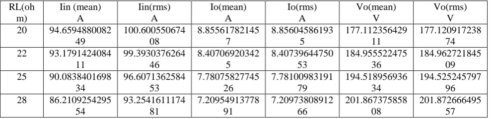
For different types of load calculating ripple factor.
RL(oh m) Iin (mean) A Iin(rms) A Io(mean) A Io(rms) A Vo(mean) V Vo(rms) V 20 94.6594880082
49 100.600550674 08 8.85561782145 7 8.85604586193 5 177.112356429 11 177.120917238 74 22 93.1791424084
11 99.3930376264 46 8.40706920342 5 8.40739644750 53 184.955522475 36 184.962721845 09 25 90.0838401698
34 96.6071362584 53 7.78075827745 26 7.78100983191 79 194.518956936 34 194.525245797 96 28 86.2109254295
54 93.2541611174 81 7.20954913778 91 7.20973808912 66 201.867375858 08 201.872666495 57
Ripple factor = Irms/Imean
For R = 20 ohm, For R =22 ohm,
Iin(rf) = 1.062762463 Iin(rf) = 1.06668762
Io(rf) = 1.000048335 Io(rf) = 1.000038925 Vo(rf) = 1.000048335 Vo(rf) = 1.000038925 For R = 25 ohm, For R = 28 ohm,
Iin(rf) = 1.07241361 Iin(rf) = 1.081697716 Io(rf) = 1.00003233 Io(rf) = 1.000026209 Vo(rf) = 1.00003233 Vo(rf) = 1.000026208
VII.CONCLUSION
High step-up inter leaved boost converter is simulated with R load. The simulation results are in line with predictions. The scope of this work is designing, modeling and simulation of ILBC. The model is developed using the blocks of Simulink. After this we conclude that interleaved boost converter provides high step up voltage 201.9v and high power 1455.70watt. and it is also minimize the ripples of output voltage and current.
VIII.FUTURE SCOPE
ISSN (Print) : 2320 – 3765 ISSN (Online): 2278 – 8875
I
nternational
J
ournal of
A
dvanced
R
esearch in
E
lectrical,
E
lectronics and
I
nstrumentation
E
ngineering
(An ISO 3297: 2007 Certified Organization) Vol. 4, Issue 2, February 2015
REFERENCES
[1] M.Subramani, Mr.K.Karthikeyan (2014) ― An Interleaved Boost DC-DC Converter for High Voltage AC and DC Applications, IJAREEIE, Vol 3, Issue 4, April 2014.
[2] R.N.A.L. Silva, G.A.L. Henn, P.P. Praca, L.H.S.C. Barreto, D.S. Oliveira Jr., F.L.M. Antunes (2008) ― Soft Switching Interleaved Boost Converter with High Voltage Gain, IEEE, 2008.
[3] Ching-Ming Lai, High-Efficiency Modular High Step-Up Interleaved Boost Converter for DC-Microgrid Applications, IEEE, Vol 48, No. 1, JANUARY/FEBRUARY 2012, Member, IEEE, Ching-Tsai Pan, Member, IEEE, and Ming-Chieh Cheng, Student Member, IEEE.
[4] S.NANGENDRA KUMAR, CHASSAN (2014) ― Modeling and Simulation of Closed Loop Control of High Voltage Gain Interleaved DC/DCConverter for RES Application, IJPSOEM, Vol 4, Issue 3, 2014.
[5] P.Radika, J.Baskaran, A.Nandhini (2014) ― High Voltage Gain Interleaved Boost Converter, IJAREEIE, Vol 3, Issue 1, January 2014.
[6] Fariborz Musavi, Member IEEE (2011) ―A High-Performance Single Phase Bridgeless Interleaved PFC Converter for Plug-in Hybrid Electric Vehicle Battery Chargers, IJAREEIE, Vol 47, NO 4, July/August 2011.