ISSN (Print) : 2320 – 3765 ISSN (Online): 2278 – 8875
I
nternational
J
ournal of
A
dvanced
R
esearch in
E
lectrical,
E
lectronics and
I
nstrumentation
E
ngineering
(An ISO 3297: 2007 Certified Organization)
Website: www.ijareeie.com
Vol. 6, Issue 3, March 2017
Design and Performance Analysis of High Pass
Filter with Modified Ground Structure for L
Band
Abhishek Singh Bhadoriya1, Sandeep Kumar Agrawal2, Mahendra Kumar Pandey3
1
PG Scholar, Department of Electronics, Rustamji Institute of Technology, BSF Academy, Tekanpur, Gwalior, India 2
Asst. Prof., Department of Electronics, Rustamji Institute of Technology, BSF Academy, Tekanpur, Gwalior, India 3
Asst. Prof., Department of Electronics, Rustamji Institute of Technology, BSF Academy, Tekanpur, Gwalior, India
ABSTRACT- The performance of a high pass filter (HPF) with and without modified ground structure for L Band telecommunication user for 1800-1900 MHz is analysed in this paper. The modified ground structure includes T etched shape in ground plane. Calculation and comparison of the response of both shaped filters was done separately. Parameters of the proposed configuration were calculated at the centre frequency of 1.48GHz and also proposed designs with dielectric constant of 4.4,loss tangent of 0.02 and substrate height of 1.6mm.Results were simulated using computer simulation technology software(CST).The undesired sidebands and fluctuations of response are reduced by using modified ground structure. Also the cut-off point of the high passes filer is shifted to a higher frequency and an improvement in selectivity.
KEYWORDS: High pass filter (HPF), Modified Ground Structure, Short circuited stub, L Band, DGS.
I.INTRODUCTION
For designing high performance and compact filters, a modified ground structure has been widely used .A modification on ground can change the propagation properties of transmission line b y changing current distribution and applied field between the ground plane and upper surface. There are various different structures f or implementing DGS[1].By using these different DGS structures filters ,power divider, power a m p l i fi er etc. was implemented [2]-[4]. PBG (photonic band-gap) and EBG (electromagnetic band-gap) structure are also a type of DGS, which is created by etching different periodic shapes in the ground plane. However, it is so difficult to use PBG structure for the design of the microwave or millimetre wave components due to the difficulties of the modulating and radiation from the periodic etched defects [5]-[9]. So many etched shapes for the microstrip could be used as a unit DGS. An LC unit circuit can represent the unit DGS circuit. They provide inductive and capacitive elements connected in series [10], which remove undesired output response fluctuations; move the high pass filter frequency limit to a higher value and the selectivity of a particular band. DGS has property of rejecting electromagnetic wave in certain frequency and direction, and most important function of these structures is the filtering of frequency bands, and harmonics of the filter in microwave.
II. IMPLEMENTATION OF 5TH ORDER HIGH PASS FILTER
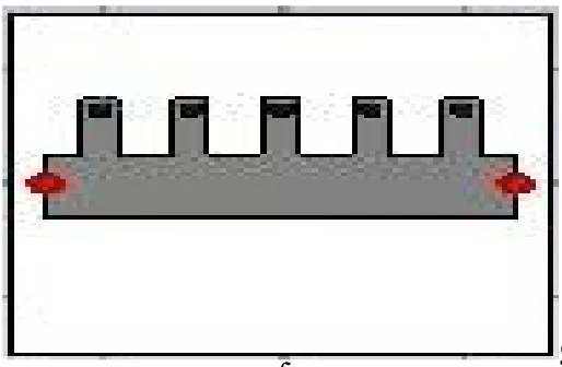
Fig-1: Optimum distributed high pass filter
To design high pass filter let us consider the cut off frequency fc=1.48GHz and 0.1dB Ripple in pass-band up to 3GHz. As in figure the electrical length Ɵc can be determined by equation (1) [12]:
−1 = 5(1)
By this, Ɵc =300 and for proposed 5th order filter shown in figure 2 which have element values given further. For given terminating impedance the associated impedance values can be determined by equation (2) and (3) [12]
= (2)
, = , (3)
For i=1, 2...6
Synthesis of W/h [12]
= (4) With
=
.
+ 0.23 + .
.
(5) Where
Zc= Zo= 50Ωandεr (dielectric constant) = 4.4, W=width, h= heightofdielectricwhichistakenas1.6mm.
Effective dielectric constant of dielectric material is given by equation (6)and(7)[12].
For w/h≤1
= + 1 + 12 . (6) For W/h>1
= + 1 + 12 . + 0.04 1− (7)
Whereas guided wavelength is given by equation (8).
=
( ) (8)
ISSN (Print) : 2320 – 3765 ISSN (Online): 2278 – 8875
I
nternational
J
ournal of
A
dvanced
R
esearch in
E
lectrical,
E
lectronics and
I
nstrumentation
E
ngineering
(An ISO 3297: 2007 Certified Organization)
Website: www.ijareeie.com
Vol. 6, Issue 3, March 2017
Ɵc=β*l (9)
Where β is the phase constant. For designing HPF T rectangular shape DGS were proposed. Length and width of rectangle is taken as 28, 11 and 7, 2mm respectively.
Fig-2: Proposed 5th order high pass filter with DGS
The element values of the proposed configuration are y1 =y2 =10mm y3 =y4=y5=10mm and y12=y23=y34=y45=6mm. And also the length between y12 and y23 is taken as 4 mm. And the rectangular hole of 2×2mm to connect PEC to the ground structure.
Fig 3(a) & 3(b) are the front view & bottom view of proposed T- shaped 5th order high pass filter.
Fig-3: (b) bottom view of the high pass filter.
The proposed DGS unit has the dimensions of L1=28mm, L2=2mm, L3=11mm and L4=7mm.
III. RESULT AND DISCUSSION
The simulation of 5th order high pass filter is shown in fig 4. FR4 (lossy) material with dielectric constant 4.4, loss tangent .02 and height of substrate 1.6mm are used in design. The graphs obtain after the simulation (CST software) of high pass filter without defected ground structure are shown in fig5.In this proposed work the result is calculated in 0-3GHz frequency range only for calculating the response of high pass filter without DGS structure of L band telecommunication user for 1800-1900 MHz
(a) (b)
(b)
Fig-4: (a) Top view of HPF (b) bottom view of HPF
ISSN (Print) : 2320 – 3765 ISSN (Online): 2278 – 8875
I
nternational
J
ournal of
A
dvanced
R
esearch in
E
lectrical,
E
lectronics and
I
nstrumentation
E
ngineering
(An ISO 3297: 2007 Certified Organization)
Website: www.ijareeie.com
Vol. 6, Issue 3, March 2017
Fig-5: Graph of HPF without DGS
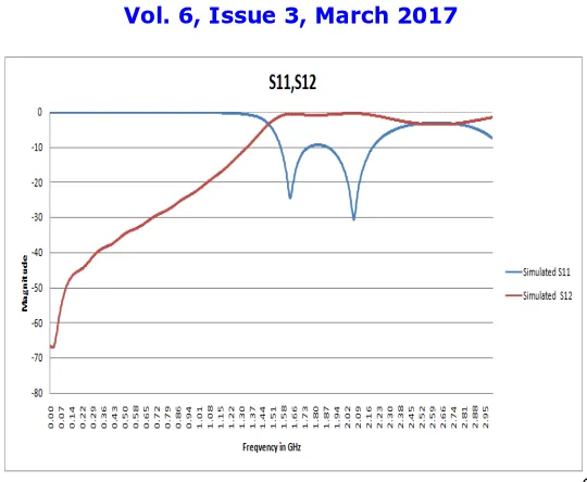
Another simulated result of using DGS (etched T shape on ground plane) is shown in figure 6. The graph shown in figure 6 after applying the DGS the cut off frequency is shifted to the 1.68GHz, which shows that the above 1.68GHz has were passes with negligible attenuation and signals below 1.68GHz is attenuation by up to 40 dB. By comparing both the results (figure 5 and figure 6), it has been found that the cut-off point changes after applying DGS and also reduced sidebands and fluctuation of the output is achieved. So for the application of L band telecommunication user for 1800-1900 MHz where we require increasing in pass-band using same size filter the use of DGS is advantageous. It shows that further improvement in the cut-off point will be achieved by using DGS in this design of high pass filter.
IV.CONCLUSION
The proposed design was implemented and analysed at the centre frequency fc=1.48GHz for HPF. It has been found that measured results are in good agreement with the simulated value. In the case of the HPF the cut-off point has been shifted to a higher frequency and sideband fluctuation was removed and also the return loss is minimized -35 to -40db. So for the application for the L band telecommunication user for 1800-1900 MHz where shifting of cut off, reduced level of fluctuation of response of HPF then use of DGS for designing filter should be proposed.
REFERENCES
[1] Mukesh Kumar Khandelwal, Binod Kumar Kanaujia, Santanu Dwari, Sachin Kumar, A.K. Gautam ’’Analysis and design of dual band compact stacked Microstrip patch antenna with defected ground structure for WLAN/WiMax applications” Journal of Electronics and Communications, Volume 69, Issue 1, Pages 39-47, January 2015.
[2] Ahmed Boutejdar, Mohamed Al Sharkawy and Abbas Omar, "A Simple Transformation of WLAN Band Pass to Low Pass Using Couple U-Defected Ground Structure (DGS) and Multilayer-Technique" Journal of Microwaves, Optoelectronics and Electromagnetic Applications, Volume 12, Issue 1, pp: 111-130, 2013.
[3] X.L. Guo, C. Xu, G.A. Zhang, Z.J. Zhang, H.H. Yin, Z.L. Wang “Tunable low-pass MEMS filter using defected ground structures (DGS)” Solid-State Electronics, Volume 94, Pages 28-31, April 2014.
[4] Dong-ming YUAN, Shu-wen ZHAO, Hong-xin ZHANG, Peng-fei HE ,“ Design and analysis of a structure-based micro strip band pass filter The Journal of China Universities of Posts and Telecommunications, Volume 21, Issue 4, August 2014, Pages 64-67,95.
[5] A.K. Verma, Ashwani kumar “Design of Low Pass Filters Using Some Defected Ground Structure” Int. J. Electron. Comm.. (AEU) 65, 2012 [6] J.-K.Xiao and Y.-F. Zhu “New U-Shaped DGS Band stop Filters” progress in Electromagnetic Research C, vol.25, page 179-191, 2012. [7] Jian-Kang Xiao, Yu-Feng Zhu “Multi-band band stop filter using inner T-shaped defected microstrip structure (DMS)” - International Journal
of Electronics and Communications, Volume 68, Issue 2, Pages 90-96,February 2014.
[8] Deena A. Salem, Ashraf. S. Mohra, A. Sebak “A compact ultra wideband band pass filter using arrow coupled lines with defected ground structure” Journal of Electrical Systems and Information Technology, Volume 1, Issue 1, Pages 36-44 May 2014.
[9] Kamaljeet Singh and K. Nagachenchaiah “Very Wideband, Compact MicrostripBand stop filter Covering S-Band to Ku-Band”. International Journal of Microwave Science and Technology H.P.Corporation Volume 2010.
[10] David M. Pozar, “Microwave Engineering”, 3rd Ed., John Wiley & Sons Inc., New York, 2005.
[11] Chang Chen, Weidong Chen, and Zhongxiang Zhang “A Novel Dual-Mode Band pass Filter with DGS” progress in Electromagnetic Research Symposium Proceedings, Marrakesh, Morocco, 2011.