IJEDR1401095
International Journal of Engineering Development and Research (www.ijedr.org)532
Design and Implementation of High Gain, High
Bandwidth CMOS Folded cascode
Operational Transconductance Amplifier
Jalpa solanki,
P.G Student,
Electronics and communication, SPCE – Visnagar, India [email protected]
________________________________________________________________________________________________________ Abstract— This paper deals with design and analysis of CMOS folded-cascode operational transconductance amplifier. Operational transconductance Amplifier (OTA) is a fundamental building block of analog circuits and systems which were previously implemented by using OPAMP. First description of optimum OTA architecture is given to optimize transistor sizing. Second, a design of folded cascode OTA, which is useful in high frequency applications like RF application. In order to implement higher frequency application, we need OTAs which have both high (DC) gain and a high bandwidth. The designed folded-cascode OTA are implemented in 0.13µm CMOS process with BSIM3V3 level 49 MOSFET model and simulation results are performed using SPICE software. From it is found that designed folded cascode OTA has a 53.99dB DC gain, around 351 MHz unity gain bandwidth and 53° phase margin.
Index Term- Folded-cascode OTA, Unity gain bandwidth, Op-amp,
I. INTRODUCTION
The design automation of analog integrated circuits is a demanding task in microelectronics industry due to the crescent necessity for low power design and time to market. The objective of analog circuit design is to map signal conditioning constrains into electronic circuit blocks that meet those specifications. This task is a challenging activity because the analog design procedure targets complex design specifications like dynamic range, noise, offset voltages, gain, etc. These parameters are closely related to transistor sizing, device technology dependent. So design process imposes to designers to make some choices based on their experience to achieve successful design.
Today operational amplifiers (OPAMPs) are used to implement variety of analog applications such as amplifiers, summers, integrators, differentiators, filters and oscillators. OPAMPs work well for low-frequency applications, such as audio and video systems but for higher frequencies, OPAMP designs become difficult due to their frequency limit [6].At those high frequencies, operational transconductance amplifiers (OTAs) are deemed to be promising to replace OPAMPS as the building blocks.
This paper is organized as follows. An Optimum Architecture of OTA was introduced in section II. Section III describes design of this OTA, Section IV present simulation results, section V shows comparative analysis with previous work while section VI provides concluding remarks.
.
II.OPTIMUMOTAARCHITECTURE
Several issues exist for selecting optimum architecture. Choice aimed both at large gain and large bandwidth. In order to achieve high gain, the differential telescopic topologies can be used. The telescopic architecture has low power consumption and it is a low noise OTA but Limited output swing and difficulty in shorting the input and output are two main drawback of this architecture [15].
In order to overcome some of the drawbacks of telescopic OTA, a folded cascode OTA based on cascode current mirror can be used. This OTA has good power supply rejection ratio (PSRR) compared to two stage OTA since the OTA is compensated with load capacitance.
A.Folded cascode OTA
The Operational Transconductance amplifiers (OTA’s) are important building blocks for various analog circuits and systems which were previously implemented by using OPAMP. OTA is an amplifier whose differential input voltage produces an output current and hence it is a voltage controlled current source.OTA is an OP-amp without an output buffer and can drive capacitive loads.
An OTA is amplifier whose all nodes are at low impedance except input and output nodes. Transconductance of OTA can be adjusted by bias current. The performance of OTA is limited by its input and output swing. To overcome these limits of simple OTA, folded cascode OTA is used.
Folded cascode OTA is shown in Fig 1. The name “folded cascode” comes from folding down n-channel cascode active loads of a diff-pair and changing the MOSFETs to p-channels.
IJEDR1401095
International Journal of Engineering Development and Research (www.ijedr.org)533
NMOS pair does. This is due to the greater mobility of NMOS device [5]. The first stage should provide the largest gain, so NMOS transistor has been chosen.B.Circuit Analysis
The Folded cascode OTA has a differential stage consisting of NMOS transistors M1 and M2. MOSFETS M3 and M4 Provide
the DC bias voltages to M5-M6-M7-M8 transistors.
Apply AC input Voltage between V+ and V-, cause the diff-amplifier drain current to become gmVin. This AC differential drain current is mirrored in the cascaded MOSFETs M9 to M12.
Figure1. Folded cascode OTA [14]
The output Voltage of the OTA is given by:
Vout = gm Vin Ro (1)
The “Unity gain frequency” of the OTA is:
Fu = gm1/2∏CL (2)
Transconductance of OTA is computed as
gm= 2∏ GBWCL (3)
The open-loop voltage gain is given by: Av = {gm1 gm8 gm10}/ ID
2
(gm8λP2 + gm10λ N2) (4)
Where, gm1, gm8 and gm10 are respectively the transconductances of transistors M1, M8 and M10. ID is the bias current
flowing in MOSFETs M1, M8, and M10. Like, CL is the capacitance at the output node. λN andλP are the parameters related to channel length modulation respectively for NMOS and PMOS devices. Taking the complementarities between the Transistors M4 and M6 into account: gm8 = gm10.
The dominant pole of OTA is located at 1/2∏ RoCL. Parasitic poles exist at the sources of M7/M8 and M9/M10.These parasitic
pole should be larger than the unity gain frequency of OTA.
III. DESIGN OF FOLDED CASCODE OTA
Based on design steps, following dimensions are found.
Table 1:- Device dimensions
M9, M10, M11, M12 2.52μm
Table 2:-Specifications
Gain 60dB
Unity gain bandwidth 300MHz
Phase margin 55°
Load capacitance(CL) 0.1pF
IJEDR1401095
International Journal of Engineering Development and Research (www.ijedr.org)534
THE DESIGNED FOLDED CASCODE OTA WAS BIASED AT 1.2V POWER SUPPLY VOLTAGE USING CMOS TECHNOLOGY OF
0.13ΜM WITH THE BSIM3V3 LEVEL 49 MOSFET MODEL
IV. SIMULATION RESULT
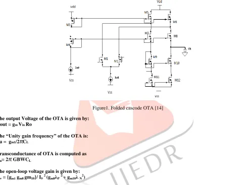
Figure 2:- gain, unity gain bandwidth
Figure 3. Phase Margin
Simulation result of Common Mode gain is shown in figure 4. From this we can get CMRR is 127.71dB
Figure 4. Common mode gain
IJEDR1401095
International Journal of Engineering Development and Research (www.ijedr.org)535
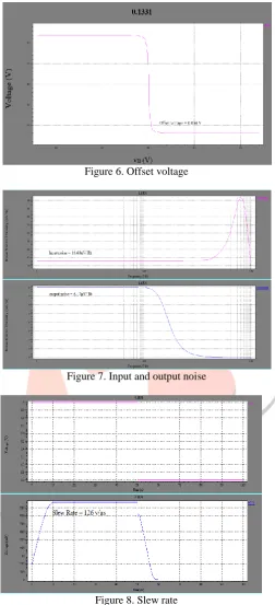
Figure 6. Offset voltageFigure 7. Input and output noise
Figure 8. Slew rate V. COMPARATIVE ANALYSIS
Parameter [1] [2] [3] [4] [7] [8] [9] [10] [11] [12] Proposed work Technology(µm) 0.18 0.18 0.18 0.18 0.18 0.18 0.18 0.18 0.18 0.18 0.13
Dc gain(dB) 68 80 95 71.7 46 80 - 76.26 62 70.02 53.99
UGB(MHz) 93.3 50 312 159 70.7 200 10 291 218.3 14.98 351
Phase
margin(Degree)
80 58 56 70.3 83.6 89 - 79.88 79.3 78.76 53
IJEDR1401095
International Journal of Engineering Development and Research (www.ijedr.org)536
VI.CONCLUSIONANDFUTURESCOPE
This work presents a design method of CMOS Folded- cascode OTA in BSIM3V3 0.13μm technology. Behavioral simulation show that designed OTA achieves High gain and High unity gain bandwidth for ±1.2V power supply. This high bandwidth Folded-cascode OTA is very useful in the high bandwidth applications like RF application.
Future work would involve measurement of parameters using PMOS and PMOS║NMOS differential pair in place of NMOS differential pair, layout, implementation of same design using gm/ID methodology and to find percentage of variation in W/L and
parameters with same specification..
REFERENCES
[1] Jonathan Rosenfeld. Mucahit Kozak, and Eby G. Friedman. A 0.8 Volt High Performance OTA Using Bulk-Driven MOSFETsfor Low Power Mmed-Signal SOCs0-7803-8182-3/03.IEEE 2003.
[2] Lei Ge and Ezz. El-hkry. A Novel Technique to Enhance the Open LoopGain of CMOS Folded Cascode OTA. 0-7803-8322-2/04.IEEE 2004.
[3] 'Ali Meaamar, 1Masuri Bin Othman, 2Omid Shoaei, A 0.1 8pim, 1.8-V CMOS High Gain Fully Differential Opamp Utilized in Pipelined ADC.0-7803-9731-2/06 IEEE2006.
[4] S. Alireza Zabihian and Reza Lotfi. Ultra-Low-Voltage, Low-Power, High-Speed Operational Amplifiers Using Body-Driven Gain-Boosting Technique. 1-4244-0921-7/07.IEEE 2007.
[5] H.Daoud, S.Bennour, M.Fakhfakh, M.Loulou.Optimizing CMOS Operational Transconductance Amplifier through Heuristic Programming. International conference on Design And Technology of Integrated system.978-1-4222-1577-9/08.IEEE 2008.
[6] You Zheng, “Operational Transconductance Amplifiers for Gigahertz applications” Queen’s University Kingston, Ontario, Canada, September, 2008.
[7] Rida S. Assaad, Student Member, IEEE, and Jose Silva-Martinez, Senior Member, IEEE. The Recycling Folded Cascode: A General Enhancement of the Folded Cascode Amplifier. IEEE journal of solid-state circuits, vol. 44, no. 9,september 2009. [8] HaidongLiu, Xiaohong Peng, Wuchen Wu. Design of a Gm-C Low Pass Filter with Low CutoffFrequency.
978-1-4244-4669-8/09.IEEE 2009.
[9] Wan Irfaan Wan Fuad and Abdul Halim Ali. Analysis of CMOS Differential Input to Increase ICMR of Folded Cascode Operational Amplifier.IEEE symposium on industial elecronics and application.2010
[10]Tapsi singh, Manjit Kaur, Gurmohan singh. Design and analysis of CMOS Folded cascode OTA using Gm/ID Technique.International Journal of Electronics and computer science engineering.2012
[11]S.Kumaravel, B.Venkataramani, S.Rishi, V.Sri Vijay,B.Shailendra. An Enhanced Folded Cascode OTA with push pull Input Stage. 978-1-4673-1591-3/12.IEEE2012 .
[12]Lucas C. Severo and Alessandro Girardi.A Methodology for the Automatic Design of Operational Amplifiers Including Yield Optimization 978-1-4799-1132-5/13 IEEE 2013.
[13]Douglas R. Holberg, Phillip E. Allen “CMOS Analog Circuit Design”
[14]R. Jacob Baker, Harry W. Li & David E. Boyce, “CMOS circuit Design, layout and simulation”, IEEE Press Series on Microelectronic Systems, Prentice Hall of India Private Limited, 2004.
[15]Behzad Razavi “Design of Analog CMOS Integrated Circuit”, Tata McGraw- Hill Edition, ISBN 0-07-052903-5.
CL( pF) - 0.18 2 2.2 5.6 1 - 0.1 1 3 0.1
Supply voltage(v)
0.8 1 1.8 1 1.8 1.8 2.7 2 1.8 1.8 1.2
CMRR(dB) - - 70 - - - 127.71
Output swing - - - 0.9 - - - -1.19 V to 1.19 V
Offset voltage(V) - - - 0.079 - - - 0.034
Input noise spectral density
- - - 16.63nV/ Rt
Output noise spectral density