A NOVEL LOW PASS FILTER USING ELLIPTIC SHAPE DEFECTED GROUND STRUCTURE
X. Q. Chen, R. Li, S. J. Shi, Q. Wang, L. Xu, andX. W. Shi
National Key Laboratory of Antennas and Microwave Technology Xidian University
Xi’an 710071,Shaanxi,China
Abstract—This paper presents a novel elliptic shape defected ground structure (DGS) for low pass filter (LPF) applications. An equivalent RLC circuit model is presented and its corresponding parameters are also extracted from the measured S-parameters. The filter presents the advantages of compact size,high selectivity; low insertion loss and high out-band suppression from 5.15 GHz to 10 GHz below −31 dB. Good agreement with response of equivalent circuit,electromagnetic simulation,and measurement is demonstrated
1. INTRODUCTION
Recently,defected ground structure (DGS) has become one of the most interesting areas of research in microwave and millimeter wave applications [1]. It could be widely used in microwave circuit design such as power divider,power amplifier and especially in filter design [1–9]. Low pass filters (LPF) design require that both in-band and out-band performances should be: low loss,high selectivity,high rejection,and wide spurious free frequency ranges. Many novel types of microstrip filters have been proposed and designed. Periodic or non-periodic DGS are realized by etching a slot in the backside metallic ground plane. The etched slot disturbs effectively the current distribution in the ground plane of microstrip line and the results in resonant characteristics [10,11].
proposed for the LPF design. The use of elliptic shape DGS will be shown to give sharp cut off frequency response as well as a good performance in both the passband and the stopband. The analysis of the dimension parameters with different dimension parameters was demonstrated as a design guide. The equivalent circuit (EC) has been extracted to characterize the proposed low-pass filter. The equivalent circuit model agrees with the field simulation results. The theoretical and measured results are presented with good agreement for LPF fabrication.
2. ELLIPTIC SHAPE DGS LOW PASS FILTER
2.1. DGS Cell andEquivalent Circuit
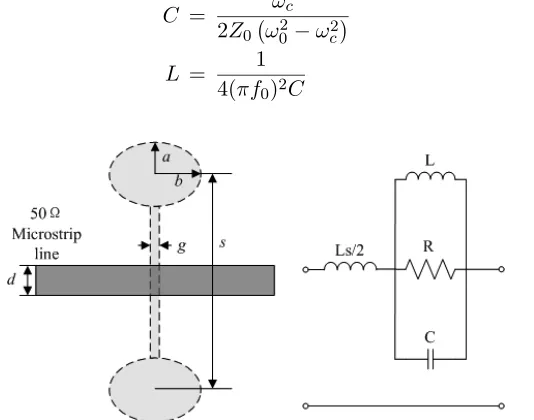
The proposed DGS cell is obtained by etching a slot connecting with two elliptic shapes defected structure in the ground plane,as shown in Figure 1. The width of microstrip line on the top is 1.88 mm,which corresponds to 50 Ω characteristic impedance. And its equivalent circuit of the cell is proposed. To derive the equivalent network parameters,the S-parameters of a DGS cell at the reference plane should be calculated using EM-simulator. And then,by using the relationship between the S parameter,the equivalent network parameters can be extracted as follows [11]:
C = ωc
2Z0
ω2 0−ωc2
(1)
L = 1
4(πf0)2C
(2)
R= 2Z0 1
|S11(ω0)|2 −
2Z0
ω0C−
1 ω0L
2
−1
(3)
where ω0 is the angular resonance frequency, ωc is the 3-dB cutoff
frequency,and Z0 is the characteristic impedance of the microstrip
transmission line.
As it is known,there is a close relationship between the etched shapes of the DGS and its frequency characteristics. Here a comparison between three types of DGS structure including dumbbell,circular and elliptic shape were carried out and simulated to identify their characteristics. The DGS cells have been simulated using HFSS and the permittivity of the dielectric board is 3.2 and the thickness h is 0.787 mm. For the comparison study of the properties,three types of DGS cell have the same defected areas of 15.1 mm2,slot length s= 12 mm and slot width g = 0.2 mm,where the elliptic shape with radius a= 2 mm and b = 2.4 mm was replace by circular shape with radius of 2.19 mm and dumbbell shape with square length of 3.88 mm. Figure 2 shows the similar characteristic curves of the proposed DGS cell.
Figure 2. Comparison of three types of DGS cell of elliptic,dumbbell and circular shapes.
Table 1. Comparison of characteristic of DGS cell. Elliptic Dumbbell Circular
fc(GHz) 3.25 3.32 3.44
f0(GHz) 5.01 5.12 5.18
L(nH) 2.833 2.579 2.581
C(pF) 0.358 0.375 0.366
S21max(dB) -27.85 -27.58 -26.93
For the elliptic DGS cell,its resonant characteristics are mainly affected by its radiusaand b. Figure 3 shows the frequency responses of EM simulation for the elliptic DGS with different radius b. The radius b varies from 1 mm to 4 mm,while radiusa= 2 mm,slot length s= 12 mm,slot widthg = 0.2 mm are constant. The variation of the characteristics could be explained by its equivalent circuit model. It demonstrates that the value of the equivalent inductance L increases as the radius b increasing from 1 mm to 4 mm,while has relatively little effect on the equivalent capacitance C. And the attenuation pole shifts from 6.28 GHz to 4.32 GHz. This causes the equivalent inductance increases proportion to the areas of the defected rectangle. And these make well explain for the shift of the cutoff frequency and the attenuation poles with changing the dimension parameters of the DGS which closely affect the values of the equivalent parameters.
2.2. Low-Pass Filter Design andOptimization
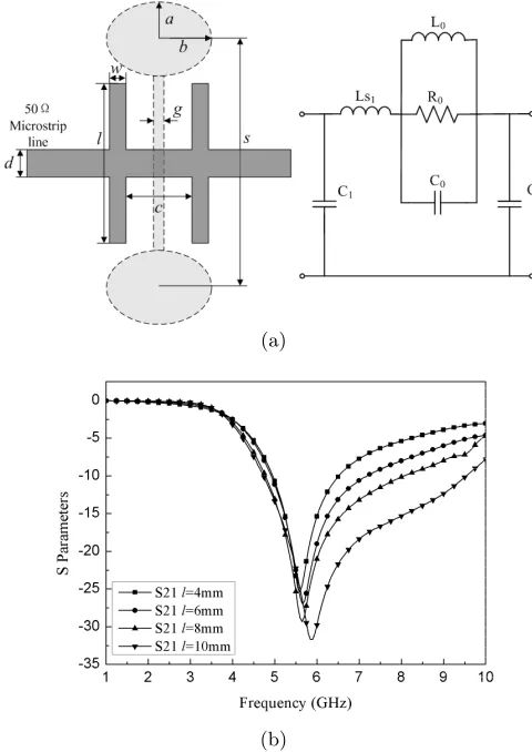
As analyzed above,the elliptic DGS can be used for low-pass filter design and spurious passband suppression. However,this structure also has some disadvantages such as insufficient suppression in high frequency range and slow cutoff characteristic. Therefore,an H shape open stubs are used in the single DGS cell to increase coupling capacitance between the microstrip line and the elliptic DGS which could minimize the size of the LPF and improve the stopband performance. Figure 4(a) shows proposed structure the LPF with H shape open stubs which parameters are c = 2.6 mm, w = 1 mm,
(a)
(b)
a= 1 mm,b= 1.5 mm andd= 1.88 mm as constant. Figure 4(b) shows the simulated results with stub length l varies from 4 mm to 10 mm. As open stub length l increased,the equivalent parallel capacitance C1 increases and the outband suppression could be improved and the attenuation pole is deeper without changing the 3 dB cutoff frequency at 3.98 GHz. And the outband suppression was improved about 15 dB when the stub length l of 10 mm compared with 4 mm.
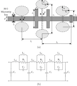
To design the desired low pass filter and improve the out band suppression,more DGS cells should be increased. The proposed low pass filter with optimized dimensions based on the analysis of single cells was proposed whit its equivalent circuit as Figure 5 shown. The dimension parameters are all constant except the open stub l2. The
value of the parameters are a = 1 mm, b = 1.5 mm, b1 = 2 mm,
w = 1 mm, g = 0.2 mm, s1 = 12 mm, s2 = 6 mm, l1 = 10 mm,
l3= 5 mm and l4 = 8 mm.
(a)
(b)
Figure 6. Simulated results of the proposed LPF with varied l2.
Figure 6 shows the simulated results of proposed low pass filter with different length of the open stub l2. When the length of stub
l2 increases,its parallel equivalent capacitance C3 which is shown in
Figure 5(b) increases too. The increased of C3 makes the out-band
suppression become lower which improves from−25 dB to−37 dB and the passband to stopband attenuation slope become sharper. While it is note that the in-band performances including insertion loss and return loss get worse at the same time. So the performances both of the passband and stopband should be concerned at the same time,and the tradeoff design method should be taken.
It means that the equivalent parallel capacitance C3 should be
chosen properly. So the parameters of the low-pass filter could be controlled and optimized by adjusting the stub length l2 with proper
length. The EM and the EC simulated results of the LPF with optimized dimensions l2 = 3 mm based on three elliptic DGS cell was
proposed as shown in Figure 7. These values of parameter in the equivalent network are: C0 = 0.43 pF, L0 = 2.21 nH, R0 = 2.192 kΩ,
C2 = 0.21 pF, L2 = 0.93 nH, R2 = 1.642 kΩ, Ls1 = 1.13 nH, Ls2 =
2.38 nH, C1 = 1.41 pF and C3 = 0.56 pF. The validity of the EM
Figure 7. The proposed LPF with EM and EC simulated results.
3. IMPLEMENTATION AND RESULTS
To validate the proposed low pass filter,it was simulated and fabricated with Taconic TLC which has relative a permittivity εr = 3.2 and a
thickness h = 0.787 mm. Figure 8(a) shows the photograph of the proposed low pass filter with compact size of 25 mm×40 mm. The measured results have shown a good agreement with the theoretical results. The experiment results show that the fabricated LPF has a 3 dB cut off frequency at 4.5 GHz and there is a shift of cut off frequency about 50 MHz. The insertion loss in the passband is low and its stopband is well suppressed below −32 dB from 5.2 GHz to 10 GHz.
(b)
Figure 8. Experiment results (a) Photograph of the proposed low-pass filter,(b) comparison of the simulated and measured results.
4. CONCLUSIONS
In this paper,a novel compact microstrip low-pass filter using elliptic DGS cells is presented. The novel H shape open stub increases the equivalent parallel capacitance to improve the outband suppression. An equivalent circuit model was given to depict the novel DGS filter. The proposed structure with main dimension parameters was analyzed as a design guide to fabricate the filter. The measurement results have shown good agreement with the theoretical results. The proposed LPF has sharp cut off frequency response,low insertion loss,and good rejection in stopband from 5.17 GHz to 10 GHz which was suppressed below−32 dB.
REFERENCES
1. Park,J.,J. P. Kim,and S. Nam,“Design of a novel harmonic-suppressed microstrip low-pass filter,” IEEE Microw. Wirel.
Compon. Lett.,Vol. 17,No. 6,424–426,2007.
2. Shobeyri,M. and M. H. Vadjed-Samiei,“Compact ultra-wideband bandpass filter with defected ground structure,” Progress In Electromagnetics Research Letters,Vol. 4,25–31,2008.
UWB bandpass filters with circular slots in ground,” Progress In Electromagnetics Research Letters,Vol. 3,87–93,2008.
4. Oraizi,H. and M. S. Esfahlan,“Miniaturization of Wilkinson power dividers by using defected ground structures,” Progress In Electromagnetics Research Letters,Vol. 4,113–120,2008.
5. Chen,X.-Q.,X.-W. Shi,Y.-C. Guo,and M.-X. Xiao,“A novel dual band transmitter using microstrip defected ground structure,” Progress In Electromagnetics Research Letters,Vol. 4,113–120, 2008.
6. Oskouei,H. D.,K. Forooraghi,and M. Hakkak,“Guided and leaky wave characteristics of periodic defected ground structures,” Progress In Electromagnetics Research,PIER 73,15–27,2007. 7. Chen,J.,Z.-B. Weng,Y.-C. Jiao,and F.-S. Zhang,“Lowpass filter
design of Hilbert curve ring defected ground structure,”Progress
In Electromagnetics Research,PIER 70,269–280,2007.
8. Sharma,R.,T. Chakravarty,S. Bhooshan,and A. B. Bhat-tacharyya,“Design of a novel 3 db microstrip backward wave cou-pler using defected ground structure,”Progress In
Electromagnet-ics Research,PIER 65,261–273,2006.
9. Zhang,F. and C. F. Li,“Power divider with microstrip electro-magnetic bandgap element for miniaturisation and harmonic re-jection,” Electron. Lett.,Vol. 44,No. 6,422–424,2008.
10. Hong,J. S. and B. M. Karyamapudi,“A general circuit model for defected ground structure’s in planar transmission lines,” IEEE Microw. Wirel. Compon. Lett.,Vol. 15,No. 10,706–708,2005. 11. Ahn,D.,J. S. Park,C. S. Kim,J. Kim,Y. X. Qian,and T. Itoh,
“A design of the low-pass filter using the novel microstrip defected ground structure,” IEEE Trans. Microw. Theory Tech.,Vol. 49, No. 1,86–93,2001.
12. Boutejdar,A.,A. Elsherbini,and A. Ornar,“Design of a novel ultra-wide stopband lowpass filter using h-defected ground structure,” Microw. Opt. Technol. Lett.,Vol. 50,No. 3,771–775, 2008.
13. Piscarreta,D. and S. W. Ting,“Microstrip parallel coupled-line bandpass filter with selectivity improvement using u-shaped defected ground structure,”Microw. Opt. Technol. Lett.,Vol. 50, No. 4,911–915,2008.