IMPLEMENTATION OF REDUCE THE AREA- POWER
EFFICIENT FIXED-POINT LMS ADAPTIVE FILTER
WITH LOW ADAPTATION-DELAY
A.Sakthivel
1, A.Lalithakumar
2PG Scholar [VLSI], Assistant Professor, Dept. of ECE,
Muthayammal Engineering College, Namakkal, Tamilnadu, (India)
ABSTRACT
In the existing system the high amount of delay, area and power can be used. So we use a novel partial product
generator and propose a strategy for optimized balanced pipelining across the time-consuming combinational
blocks of the structure. To achieve lower adaptation-delay and area-delay-power efficient implementation proposed
technique is adapted. In proposed method we use large processing elements (PEs) for achieving a lower adaptation
delay with the critical path of one MAC operation. They have proposed a fine-grained pipelined design to limit the
critical path to the maximum of one addition time, which supports high sampling frequency, but involves a lot of
area overhead for pipelining and higher power consumption due to large number of pipeline latches. An efficient
adder tree for pipelined inner-product computation is used to minimize the critical path and silicon area without
increasing the number of adaptation delays. So we use a carry select adder in the proposed method to reduce the
area and power. The carry select adder is efficient adder and easy to design compare to other design.
Keywords:
Adaptive Filter, Least Mean Square Algorithm, Weight Update Block, AdderI INTRODUCTION
The Least Mean Square (LMS) adaptive filter is the most popular and most widely used adaptive filter because of its
satisfactory convergence performance. The direct-form LMS adaptive filter involves a long critical path due to an
inner-product computation to obtain the filter output. The critical path is reduced by pipelined implementation .the
conventional LMS algorithm does not support pipelined implementation because of its recursive behavior, It is
modified then it called by delayed LMS (DLMS) algorithm which allows pipelined implementation of the filter. A
lot of work has been done to implement the DLMS algorithm in systolic architectures to increase the maximum
usable frequency but, they involve an adaptation delay of ∼ N cycles for filter length N, which is quite high for large
order filters. Since the convergence performance degrades considerably for a large adaptation delay has proposed a
modified systolic architecture to reduce the adaptation delay.
A transpose-form LMS adaptive filter, where the filter output at any instant depends on the delayed versions of
large processing elements (PEs) for achieving a lower adaptation delay with the critical path of one MAC operation.
A fine-grained pipelined design to limit the critical path to the maximum of one addition time, which supports high
sampling frequency, but involves a lot of area overhead for pipelining and higher power consumption than due to its
large number of pipeline latches. Further effort has been made to reduce the number of adaptation delays. With an
efficient adder tree for pipelined inner-product computation to minimize the critical path and silicon area without
increasing the number of adaptation delays.
Adaptive digital filters have a wide range of communication in area and DSP applications such as adaptive
equalization, system identification, and image restoration and noise cancelling and flip-flop clustering. In adaptive
filter mostly used algorithm is the least mean-square (LMS) algorithm because of its extra performance and simple
calculation.
II EXISTING METHOD
An efficient architecture is used for the implementation of a delayed least mean square adaptive filter. We use novel
partial product generator to optimized balanced pipelining across the time-consuming combinational blocks of the
structure. We also find that the proposed design offers less area, less energy than the best of the existing systolic
structures, on average, for filter lengths N = 8.The proposed structure for the weight-update block is shown in
below. It performs N multiply-accumulate operations of the form (μ × e) × xi + wi to update N filter weights for
each condition. Every the MAC units performs the multiplication of the shifted value of error with the delayed input
samples xi followed by the additions with the corresponding old weights. All the N multiplications for the MAC
operations are performed by N PPGs, followed by N shift–add trees. The PPGs generates L/2 partial products
corresponding to the each product of the recently shifted error value μ × e with L/2, the number of 2-b digits of the
input word xi.
Since the scaled error (μ×e) is multiplied with the entire N delayed input values. This leads to substantial reduction
of the adder complexity. The final outputs of MA units calculated and the desired updated weights to be used as
inputs of the error-computation block as well as the weight-update block for the next iteration. The weight-update
block generates w n−1−n2, and the weights are delayed by each of n2+1 cycle. However, it should be noted that the
delay by 1 cycle is due to the latch, which is included in the delay of the error-computation block, i.e.n1. Therefore,
the delay generated in the weight-update block becomes n2. If the locations of pipeline latches are decided n1
becomes 5, where three latches are in the error-computation block, one latch is after the subtraction and the other
latch is before PPG Also, n2 is set to 1 from a latch in the shift-add tree in the weight-update block.
III PROPOSED METHOD
3.1 Carry Select Adder
A carry-select adderis a way to implement an adder, it is easy to design. In logic element that computes the -bit sum
adders and a multiplexer. Adding two n-bit numbers with a carry-select adder is done with two adders (therefore two
ripple carry adders) in order to perform the calculation twice, The each of the function each of carry being zero and
the other assuming one.
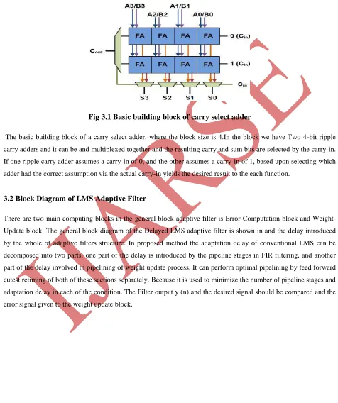
Fig 3.1 Basic building block of carry select adder
The basic building block of a carry select adder, where the block size is 4.In the block we have Two 4-bit ripple
carry adders and it can be and multiplexed together and the resulting carry and sum bits are selected by the carry-in.
If one ripple carry adder assumes a carry-in of 0, and the other assumes a carry-in of 1, based upon selecting which
adder had the correct assumption via the actual carry-in yields the desired result to the each function.
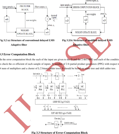
3.2 Block Diagram of LMS Adaptive Filter
There are two main computing blocks in the general block adaptive filter is Error-Computation block and
Weight-Update block. The general block diagram of the Delayed LMS adaptive filter is shown in and the delay introduced
by the whole of adaptive filters structure. In proposed method the adaptation delay of conventional LMS can be
decomposed into two parts: one part of the delay is introduced by the pipeline stages in FIR filtering, and another
part of the delay involved in pipelining of weight update process. It can perform optimal pipelining by feed forward
cutest retiming of both of these sections separately. Because it is used to minimize the number of pipeline stages and
adaptation delay in each of the condition. The Filter output y (n) and the desired signal should be compared and the
Fig 3.2 (a) Structure of conventional delayed LMS Fig 3.2(b) Structure of modified delayed LMS
Adaptive filter Adaptive filter
3.3 Error Computation Block
In the error computation block the each of the input are given to the D and the 2-BIT PPG and each of the condition
to check the co efficient of each sample of inputs. N number of 2-b partial product generators (PPG) with respect to
N num of multipliers and a cluster of L/2 binary adder trees. It should be based on adder tree and shift adder tree.
Fig 3.3 Structure of Error-Computation Block
3.4 Structure of PPG
In the PPG L/2 number of 2-to-3 decoders and also the same number of AND/OR cells (AOC).the 2 to 3 decoders
Fig3.4 Structure of PPG (AOC stands for OR/AND cell
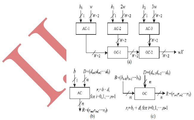
3.5 Structure of AOC
The structure of AOC consists of three AND cells and two OR cells. The each of the function can perform each
operation separately. Each AND cell takes an n-bit input D and a single bit input b, and also consists of n AND
gates.
Fig 3.5 Structure and function of AND/OR cell.
The each of the b0 input fed to the AC-1 and b1 and b2 are respectively to the AC-2 and AC-3.the AC-1 to
compare the these two inputs and give the result to the OC-1.D=(dn-1,dn-2…d0) and B=( bn-1,bn-2…b0) , R=(
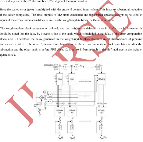
3.6 Weight-Update Block
The proposed structure for the weight-update block is shown in below. It performs N multiply-accumulate
operations of the form (μ × e) × xi + wi to update N filter weights for each condition. Every the MAC units performs
the multiplication of the shifted value of error with the delayed input samples xi followed by the additions with the
corresponding old weights. All the N multiplications for the MAC operations are performed by N PPGs, followed by
N shift–add trees. The PPGs generates L/2 partial products corresponding to the each product of the recently shifted
error value μ × e with L/2, the number of 2-b digits of the input word xi.
Since the scaled error (μ×e) is multiplied with the entire N delayed input values. This leads to substantial reduction
of the adder complexity. The final outputs of MA units calculated and the desired updated weights to be used as
inputs of the error-computation block as well as the weight-update block for the next iteration.
The weight-update block generates w n−1−n2, and the weights are delayed by each of n2+1 cycle. However, it
should be noted that the delay by 1 cycle is due to the latch, which is included in the delay of the error-computation
block, i.e.n1. Therefore, the delay generated in the weight-update block becomes n2. If the locations of pipeline
latches are decided n1 becomes 5, where three latches are in the error-computation block, one latch is after the
subtraction and the other latch is before PPG Also, n2 is set to 1 from a latch in the shift-add tree in the
weight-update block.
IV EXPERIMENTAL RESULTS AND DISCUSSIONS
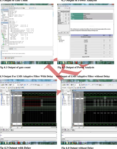
4.1 Output of Gate Count
4.2 Output of Power Analysis
Fig 4.1 Output of gate count Fig 4.2 Output of Power Analysis
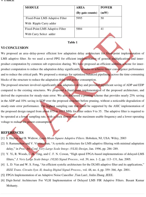
4.3 Output For LMS Adaptive Filter With Delay 4.4 Ouput of LMS Adaptive Filter without Delay
V TABLE
Table 1
VI CONCLUSION
We proposed an area–delay-power efficient low adaptation delay architecture for fixed-point implementation of
LMS adaptive filter. So we used a novel PPG for efficient implementation of general multiplications and
product computation by common sub expression sharing. We have proposed an efficient addition scheme for
inner-product computation to reduce the adaptation delay significantly in order to achieve faster convergence performance
and to reduce the critical path. We proposed a strategy for optimized balanced pipelining across the time-consuming
blocks of the structure to reduce the adaptation delay and power consumption.
The proposed structure involved significantly less adaptation delay and provided significant saving of ADP and EDP
compared to the existing structures. We proposed a fixed-point implementation of the proposed architecture, and
derived the expression for steady-state error. We also discussed a pruning scheme that provides nearly 25% saving
in the ADP and 10% saving in EDP over the proposed structure before pruning, without a noticeable degradation of
steady-state error performance. The highest sampling rate that could be supported by the ASIC implementation of
the proposed design ranged from about 875 to 1015 MHz for filter orders 9 to 35. The adaptive filter is required to
be operated at a lower sampling rate, with a clock slower than the maximum usable frequency and a lower operating
voltage to reduce the power consumption.
REFERENCES
[1] S. Haykin and B. Widrow, Least-Mean-Square Adaptive Filters. Hoboken, NJ, USA: Wiley, 2003
[2] S. Ramanathan and V. Visvanathan, “A systolic architecture for LMS adaptive filtering with minimal adaptation
delay,” in Proc.Int. Conf. Very Large Scale Integr. (VLSI) Design, Jan. 1996, pp. 286–289.
[3] Y. Yi, R. Woods, L.-K. Ting, and C. F. N. Cowan, “High speed FPGA-based implementations of delayed-LMS
filters,” J. Very LargeScale Integr. (VLSI) Signal Process., vol. 39, nos. 1–2, pp. 113–131, Jan. 2005.
[4] L. D. Van and W. S. Feng, “An efficient systolic architecture for the DLMS adaptive filter and its applications,”
IEEE Trans. CircuitsSyst. II, Analog Digital Signal Process., vol. 48, no. 4, pp. 359–366, Apr. 2001.
[5] FPGA Implementation of an Adaptive Noise Canceller ,Tian Lan1, Jinlin Zhang ,IEEE.
[6] Digit-Serial Architecture For VLSI Implementation of Delayed LMS FIR Adaptive Filters. Basant Kumar
Mohanty.
MODULE AREA
(By gate counts)
POWER
(mW)
Fixed-Point LMS Adaptive Filter
With Ripple Carry adder
5995 50
Fixed-Point LMS Adaptive Filter
With Carry Select adder