Single String Interleaved Boost Converter
Based PV Eleven Level Inverter System for
Rural Application
Nithin Shaji 1, Dr Sreekala . K 2
P.G. Student, Department of Electrical and Electronics Engineering, SNGCE, Kadayiruppu, Kerala, India1 Associate Professor, Department of Electrical and Electronics Engineering, SNGCE, Kadayiruppu, Kerala, India2
ABSTRACT: The most severe problem our society is facing now is limitation of power which we can produce with our limited sources. Non renewable sources of energy are diminishing day by day which has resulted in an increase in cost of these sources. Demand of electricity will worsen present scenario of decreasing non renewable resources. In the present scenario renewable solar energy usage is the most suitable solution. The paper presents insight into most suitable electronic conversion circuit for solar energy usage. Interleaved Boost converter circuit was used because of its parallel current operation using lower rated low cost inductors. Multilevel inverter circuitry is used for converting DC to AC. Structural configuration of PV cells and reflectors for rural are for efficient usage of sunlight is described.
KEYWORDS:PV system Fuzzy, Interleaved Boost Converter, Bi-directional switching, H Bridge Inverter.
I.INTRODUCTION
The most severe problem our society is facing now is limitation of power which we can produce. Non renewable sources of energy are diminishing day by day which has resulted in an increase in cost of these sources. Cost of electrical energy generation based on non renewable energy is affected by this. Demand of electricity will worsen present scenario of decreasing non renewable resources. In these conditions renewable energy usage is the most suitable solution available. Of the renewable energy solar is the best suitable for electricity generation.
The Block diagram of current PV DC/AC system is shown in Fig 1. PV system of single string and multi string are available. Multi string PV has a disadvantage of using multiple boost converters for boosting operation. This will increase conduction losses and switching losses of multi string PV system. So single string PV system is proposed here to be used instead of multi string.
Fig 1 Block diagram of the current system
Normal boost converter is used in current system for boosting. This system when used for high level boosting will have inductors of high rating and cost of such inductors will be high. Interleaved boost converter is proposed to be used instead of normal boost converters. The interleaved boost converter will provide parallel paths for current flow thus the inductor rating of parallel inductors can be lower than the normal inductor and size of such inductor will be smaller.
controller. Fuzzy is a tool used for manipulating imprecise data. Fuzzy based controller is intended to be used in the proposed system replacing PI for better performance.
Eleven levels multilevel inverter is proposed to be used for achieving better AC wave form. At the eleven level inverter circuitry MOSFETs will be replacing IGBT switches since the operation is well under 1000V and 5KW power MOSFET switches can replace IGBT for better conduction properties. The body diode operation of MOSFET can be used here for bidirectional switch representation instead of IGBT with bridge diode configuration. Bidirectional switch representation form of MOSFET is used for capacitor selection and H-bridge inverter is used to achieve eleven levels AC waveform.
Fig 2 Block diagram of the (proposed system) Single String Interleaved Boost Converter Based PV Eleven Level Inverter System for Rural Application
Fig 2 shows Block diagram of the single string interleaved boost converter based PV eleven level inverter systems for rural application (proposed system). Single string PV system provides a dc input to interleaved boost converter for boosting. Voltage sensors are used for regulating output voltage of interleaved boost converter through controller. The output of interleaved boost converter DC is converted to AC by multilevel inverter and fed to the load.
II.CIRCUITCONFIGURATIONOFINTERLEAVEDBOOSTCONVERTER
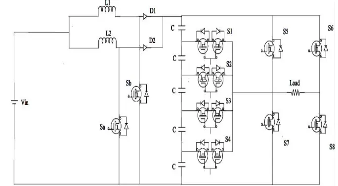
Fig 3 shows the circuit diagram of proposed single string interleaved boost converter based PV eleven level inverter systems for rural application. Here in the circuit PV module is represented by a cell. L1,Sa, D1 and L2 ,Sb,D2 form two parallel paths of interleaved boost converter. Here the switches switch to provide charging and discharging operation of the inductor. When switch Sa (Sb) is turned on then inductor L1 (L2) charges and when turned off the inductors discharges across the capacitors. The capacitor selection capacitors S1, S2, S3, and S4 are used to select intermediate levels between +V max and –V max. Switches S5, S6 , S7 and S8 form H bridge inverter circuit.
III.CIRCUITOPERATIONOFINTERLEAVEDBOOSTCONVERTER
For simplifying circuit analysis following assumptions is made: 1) Input voltage is pure sinusoidal
2) Ideal lossless components
3) Switching frequency (fs) is much higher than the ac line frequency ( )
4) Output capacitor Ci(i=1,2,3,4,5) is large enough such that the output voltage can be considered constant over the whole line period.
The switches of interleaved boost converter are operated at 50% duty ratio. Here the switches switch to provide charging and discharging operation of the inductor. When switch Sa (Sb) is turned on then inductor L1 (L2) charges and when turned off the inductors discharges across the capacitors. The operation of interleaved boost converter at 50 % duty cycle allows a constant current flow through output capacitor Co thus reducing the output voltage ripple and the inductor size is reduced as the current sharing action is taking place.
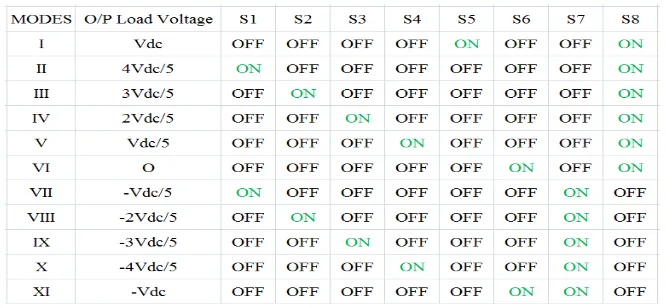
At inverter section the bi-direction MOSFET switches are triggered in appropriate intervals to provide eleven level stepped output. The proposed inverter's operation can be divided into eleven switching states. Proper switching of the inverter can produce eleven output voltage levels (Vdc , 4Vdc/5, 3Vdc/5, 2Vdc/5, Vdc/5, 0, Vdc/5, 2Vdc/5, -3Vdc/5, -4Vdc/5, - Vdc) from the dc supply voltage. There are eleven level modes of operation based on the switching conditions as shown in the TABLE IV.
Modes of operation of the system:
i.
Maximum positive output ( Vdc):Switch S5 is ON, connecting the load positive terminal to Vdc, and S8 is ON, connecting the load negative terminal to ground. All other controlled switches are OFF. The voltage applied to the load terminals is Vdc.
ii.
Four Fifth positive output (4 Vdc/5):The bidirectional switch 51 is turned ON, connecting the load positive terminal, and 58 is turned ON, connecting the load to negative terminal to ground. All other controlled switches are OFF. The voltage applied to the load terminals is 4 Vdc/5.
iii.
Third-fifth positive output (3Vdc/5):The bidirectional switch S2 is turned ON, connecting the load positive terminal, and S8 is turned ON, connecting the load negative terminal to ground. All other controlled switches are OFF. The voltage applied to the load terminals is 3Vde/5.
iv.
Two-fifth positive output (2Vdc/5):The bidirectional switch S3 is turned ON, connecting the load positive terminal, and S8 is turned ON, connecting the load negative terminal to ground. All other controlled switches are OFF. The voltage applied to the load terminals is 2Vdc/5.
v.
One Fifth positive output (Vdc/5):The bidirectional switch S4 is turned ON, connecting the load positive terminal, and S8 is turned ON, connecting the load negative terminal to ground. All other controlled switches are OFF; the voltage applied to the load terminals is Vdc/5
vi.
Zero output:This level can be produced by two switching combinations; switches S5 and S7 are ON, or S6 and S8 are ON, and all other controlled switches are OFF. The terminal a-b is a short circuited. The voltage applied to the load terminals is zero.
vii.
One-fifth negative output (-Vdc/5):The bidirectional switch S7 is ON, connecting the load positive terminal, and SI is ON, connecting the load negative terminal to Vdc. All other controlled switches are OFF. The voltage applied to the load terminals is – Vdc/5.
viii.
Two-fifth negative output (-2Vdc/5):ix.
Three-fifth negative output (-3Vdc/5):The bidirectional switch S7 is ON, connecting the load positive terminal, and S3 is ON, connecting the load negative terminal to ground. All other controlled switches are OFF; the voltage applied to the load terminals is -3 Vdc/5.
x.
Four-fifth negative output (-4Vdc/5):The bidirectional switch S7 is ON, connecting the load positive terminal, and S4 is ON, connecting the load negative terminal to ground. All other controlled switches are OFF; the voltage applied to the load terminals is -4 Vdc/5.
xi.
Maximum negative output (-Vdc):Switch S6 is ON, connecting the load negative terminal to Vdc, and S7 is ON, connecting the load positive terminal to ground. All other controlled switches are OFF. The voltage applied to the load terminals is – Vdc.
Out Put Voltages according to switches ON and OFF is shown in TABLE I
TABLE I Out Put Voltages according to switches ON and OFF
IV.DESIGN OF INTERLEAVED BOOST CONVERTER USED IN ELEVEN-LEVEL INVERTER
The Interleaved boost Converter is designed based on the following parameters Input voltage (Vdc), Output voltage (Vo), Power (Pin), Switching frequency (fs), Duty ratio (D).The Duty ratio D is given by equation,
=Vo−Vdc
Vo
Load resistance is given by equation,
= Vo
Po
Pin = Po Inductor value is given by equation,
=R⨉D⨉(1−D )
Where R = load resistance. The value of capacitor is given by,
= V × D
F⨉ΔV⨉R
Where ΔV is output ripple.
V. CONTROL SYSTEM
A. PI CONTROLLER FOR INTERLEAVED BOOST CONVERTER
Fig 4: PI controller for interleaved boost converter
The fig 4 shows the PI controller used in interleaved boost converter. The PI controller is mainly used to eliminate the steady state error resulting from P controller. It has a negative impact on the speed of response and overall stability of the system. The Controller is mostly used in areas where speed of the system is not an issue. It cannot decrease the rise time and eliminate the oscillations.
The error signal is attained by subtracting voltage output value (Vout) from reference voltage value (Vref). The error signal is given to PI controller to produce the duty cycle. The duty cycle value is then provided to the PWM gen Block. PWM Gen Block can produce three PWM signals PWM1, PWM2, PWM3. PWM1 produces PWM pulses at defined duty ratio. PWM2 and PWM3 can be phase shifted comparing to PWM1 output. Here PWM2 will produce PWM pulses at 180 phase shift compared to PWM1. PWM1 and PWM2 output pulses are used for gate triggering of switches S1 and S2.
B. FUZZZY CONTROLER FOR INTERLEAVED BOOST CONVERTER
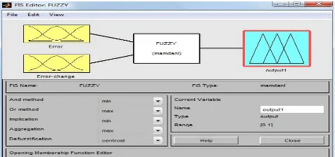
Closed loop control using FUZZY is used in this system so as to provide better and easier control. FUZZY is a tool that can manipulate imprecise data and is much simpler than its predecessors (linear algebraic equation ). In earlier system using PI controller in closed loop the output was changed in a steady value. By using triangular membership function in FUZZY mamdani model we are able relate each of the variables, i.e. error and error change in rules to provide an output. FIS editor (Fuzzy inference System editor) is used to enter variables in FUZZY and there triangular membership function (Fig 5).
Fig 6 Closed loop controller using FUZZY
Fig 6 shows the MATLAB model of closed loop controller using FUZZY mamdani model. The error signal is produced by subtracting the voltage output value of the converter with reference value of output voltage. When this error is provided to the unit delay block a change in error signal is occurred. Both this signal is given as input to mux block and the output of mux block is provided as input to FUZZY block. Output of FUZZY block will be the duty ratio. The output of FUZZY is provided as input to the PWM Gen block to produce PWM signals with
180 phase difference. These triggering pulses are provided to the switches S1 and S2. TABLE II FUZZY RULES
Table II shows FUZZY rules which shows different output values to be provided according to the error (e) and change in error (
ė)
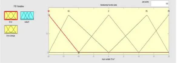
signals.Fig 7a: FUZZY variable Error and its triangular membership functions
Fig 7c: FUZZY variable output1 and its triangular membership functions
In this system five membership functions NB, NS, Z, PS, PB are used in input variables as shown in Fig 7a, 7b . So a total of twenty five rules can be created relating this to membership function of output variable output1.The membership functions of output variable output1 are NVB, NB, NM, NS, Z, PS, PM, PB, PVB as shown in Fig 7c.
VI.SIMULATION RESULT
For verifying the feasibility and validity of the proposed converter, MATLAB/SIMULINK software is applied for the simulation of the proposed system (Fig 7) with an input voltage of = 24 V at 50 kHz and output voltage of Interleaved boost converter is set as . The duty cycle of the Interleaved boost converter is set as 50%. Switching
frequency is taken at 3kHZ and ΔV at 0.01. Simulation parameters used is shown in Table III. TableIII SIMULATION PARAMETERS
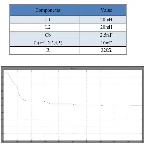
Components Value L1 20mH L2 20mH Cb 2.5mF Ci(i=1,2,3,4,5) 10mF R 320Ω
Fig 8: Output of FUZZY controller (duty cycle)
Fig 9: Single String Interleaved Boost Converter Based PV Eleven Level Inverter System For Rural Application Fig 9 shows the simulation model of Single String Interleaved Boost Converter Based PV Eleven Level Inverter System for Rural Application. A FUZZY controller was used for the closed loop simulation of interleaved boost converter of the above discussed system. The Output Voltage is compared with the reference Output voltage.
The compared Output is fed to FUZZY controller Block. The Output of the FUZZY controller is given as input to PWM Generator module with phase shift180 . This Output is fed to the gate of the MOSFET’s Sa and Sb for triggering the MOSFETS to ON condition.
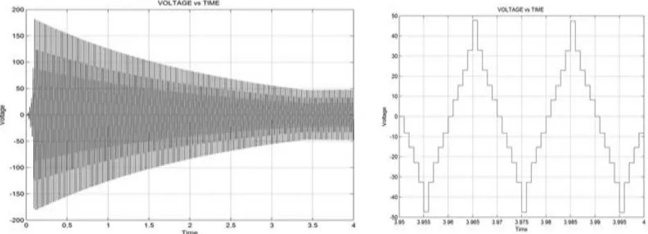
Fig 10 and 11 shows the output voltage waveform which is taken across the load resistor. The required out voltage was reached and the overshoots which is seen in PI controller is absent in the FUZZY system and the waveform generated by FUZZY is smoothly increasing to the reference value. Oscillation at the reference value is absent in FUZZY controller output while oscillation of small range was visible at PI controller output.
Fig 11: Output voltage of Single String FUZZY controlled Interleaved Boost Converter Based PV Eleven Level Inverter System For Rural Application.
VII. HARDWARE MODEL
Fig 12: Hardware model of Fuzzy controlled single string interleaved boost converter based PV eleven level inverter system for rural application
Fig 12 shows the hardware implementation of the fuzzy controlled single string interleaved boost converter based PV eleven level inverter systems for rural application. The above shown circuit consists of 10 driver circuit to switch 10 MOSFET based switches. Driver circuit is used to provide 15 volts to switch the MOSFET Switches of the inverter. Driver amplifies the voltage from microcontroller which is 5 volts. Also it has an optocoupler for isolating purpose. So damage to MOSFET is prevented. The driver circuit forms the most important part of the hardware unit because it acts as the backbone of the inverter because it gives the triggering pulse to the switches in the proper sequence.
The interleaved boost converter boosts the input voltage and the output is provided as input to the capacitor selection circuit. Where according to the switches triggered different voltage levels can be created. The output of the capacitor selection circuit is given across the H bridge inverter. The output of H Bridge inverter results in eleven level inverted output.
The optocoupler steps up PWM voltage level to Vcc (15V). These gating pulses are used to drive or switch MOSFETs. The pulse used for switching Switch Sa and Sb of interleaved boost converter are shown in fig 13. The gating pulses of MOSFETs used in capacitor selection switches are shown in fig 14 ( switches S1 and S2 ), fig 15 ( switches S3 and S4 ),fig 16 ( switches S5 and S7 ), fig 17 ( switches S6 and S8 ).
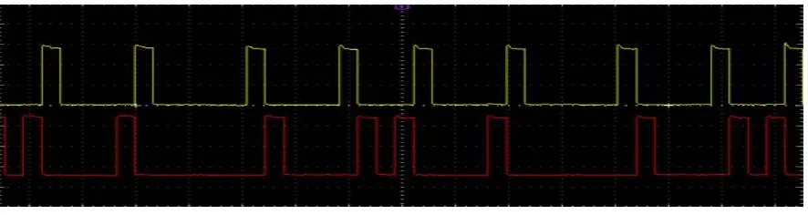
Fig 13: Gate pulses for switch Sa(Yellow) And Sb(Red)
Fig 13 shows the gating pulses provided to switches Sa and Sb. The yellow signal shows the gating pulse to switch Sa and red signal shows the gating pulses to switch Sb.
Fig 14: Gate pulses for switch S1(Yellow) And S2(Red)
Fig 14 shows the gating pulses provided to switches S1 and S2. The yellow signal shows the gating pulse to switch S1 and red signal shows the gating pulses to switch S2.
Fig 15: Gate pulses for switch S3(Yellow) And S4(Red)
Fig 16: Gate pulses for switch S7(Yellow) And S5(Red)
Fig 16 shows the gating pulses provided to switches S7 and S5. The yellow signal shows the gating pulse to switch S7 and red signal shows the gating pulses to switch S5.
Fig 17: Gate pulses for switch S6(Yellow) And S8(Red)
Fig 17 shows the gating pulses provided to switches S6 and S8. The yellow signal shows the gating pulse to switch S6 and red signal shows the gating pulses to switch S8.
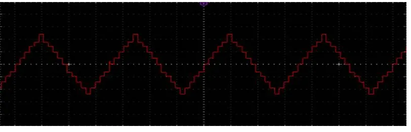
Fig 18: Output voltage waveform
Fig 18 shows the output voltage waveform of of Fuzzy controlled single string interleaved boost converter based PV eleven level inverter system for rural application taken across the load. The switches were successfully triggered and output waveform was achieved.
VIII. CONCLUSION
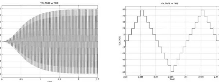
since current is split into two parallel paths. Decrease in rating will lead to lower coast as well as smaller size. The capacitor voltage ripple is also reduced as the current always passes through the capacitor charging the capacitor in case of discharge. So capacitor of lower tolerance to voltage ripple can be used. The overshoots and oscillation seen in PI controller is eliminated in this system by using of FUZZY controller. Fig 19 shows comparison between PI and FUZZY controllers. Fuzzy controller can work when value for object is uncertain.
Fig 19: Comparison between PI and FUZZY
By using MOSFET’s based bi-directional switch combination replacing IGBT and Diode bridge structure we are reducing the use of non linear structure. MOSFET’s are highly suitable for low power operation considering IGBT.
The future research will be focused on reducing no of components so as to decrease the total coast of the system. Advanced controller using neural control can be used for better performance. Research can be done for replacing series capacitor circuit since voltage division is not similar between two capacitors of same rating.
REFERENCES
[1] E.G.Chinju and S.Reshmila, “A Novel Nine Level Inverter For Photovoltaic Applications”, International Conference on Emerging Trends in Engineering & Management (ICETEM-2016)
[2] Nithin Shaji and Dr Sreekala.K, “Fuzzy controlled power factor correctionin AC/DC interleaved boost converter” ,International Conference on Circuit, Power and Computing Technologies (ICCPCT-2016)
[3] Sreevidya. E.V and V. Jegathesan, “A Modified Control Approach For Power Factor Correction In AC/DC Boost Converter” , IEEE Sponsored 2nd International Conference on Innovations in Information, Embedded and Communication systems (ICIIECS)2015
[4] VivekP. V and P. Kanakasabapathy, “Multistring Seven-Level Inverter for Standalon Photovoltaic Systems”, IEEE International Conference on Technological Advancements in Power & Energy, 2015
[5] S.Parthiban , P.G Scholar and D. Durairaj, “Standalone Photovoltaic System with MPPT Techniques on Single-Phase Eleven-Level Inverter for Utility Applications”, IEEE Trans. Ind. Electron, 2015
[6] Giampaolo Buticchi, Davide Barater, Emilio Lorenzani, Carlo Concari, and Giovanni Franceschini, “A Nine-Level Grid-Connected Converter Topology for Single-Phase Transformerless PV Systems”, IEEE Transactions On Industrial Electronics, VOL. 61, NO. 8, AUGUST 2014
[7] S .Krishnan and K. Sathiyasekar, “Modified Structure and Reflector Based SolarPhotovoltaic System for Optimization of Solar Energy”,
IEEE International Conference on Advanced Communication Control and Computing Technologies (ICACCCT) 2014
[8] Charles I. Odeh, Damian B.N. Nnadi, “Single-phase 9-level hybridised cascaded multilevel inverter”, IET Power Electron. Vol. 6, Iss. 3, pp. 468–477,2013
[9] Nasrudin A. Rahim, Krismadinata Chaniago, and Jeyraj Selvaraj, “Single-Phase Seven-Level Grid-Connected Inverter for Photovoltaic System”, IEEE Transactions On Industrial Electronics, VOL. 58, NO. 6, JUNE 2011.
[10] Elena Villanueva, Pablo Correa, José Rodríguez and Mario Pacas, “Control of a Single-Phase Cascaded H-Bridge Multilevel Inverter for Grid-Connected Photovoltaic Systems”, IEEE Transactions On Industrial Electronics, VOL. 56, NO. 11, NOVEMBER 2009
[11] Jinn-Chang Wu and Chia-Wei Chou, “A Solar Power Generation System with a Seven-Level Inverter”, IEEE Transactions On Industrial Electronics, VOL. 56, NO. 11, NOVEMBER 2009
[12] Sérgio Daher, Jürgen Schmid, and Fernando L. M. Antunes, “Multilevel Inverter Topologies for Stand-Alone PV Systems”, IEEE Transactions On Industrial Electronics, VOL. 55, NO. 7, JULY 2008
[13] Cassiano Rech, and José Renes Pinheiro, “Hybrid Multilevel Converters: Unified Analysis and Design Considerations”, IEEE Transactions On Industrial Electronics, VOL. 54, NO. 2, APRIL 2007
[14] Roberto González, Jesús López, , Pablo Sanchis, and Luis Marroyo, “Transformerless Inverter for Single-Phase Photovoltaic Systems”, IEEE Transactions On Power Electronics, VOL. 22, NO. 2, MARCH 2007
[15] Jing Huang and Keith A. Corzine, “Extended Operation of Flying Capacitor Multilevel Inverters”, IEEE Transactions On Power Electronics,, VOL. 21, NO. 1, JANUARY 2006.
[16] Feel-Soon Kang, Sung-Jun Park, Su Eog Cho,Cheul-U Kim and Toshifumi Ise, “Multilevel PWM Inverters Suitable for the Use of Stand-Alone Photovoltaic Power Systems”, IEEE Transactions On Energy Conversion, VOL. 20, NO. 4, DECEMBER 2005