Solar Power Generation Seven Level To Nine
Level Inverter
K.Srinivasulu
1
, B.Manthru Naik
2
M.Tech Student, Dept. of EEE, Dr. Samuel George Institute of Engineering &Technology, Markapur, JNTU Kakinada
University, India1
Associate Professor, Dept. of EEE, Dr. Samuel George Institute of Engineering &Technology, Markapur, JNTU
Kakinada University, India2
ABSTRACT: This paper generates a solar photovoltaic system with dc-dc power converter and a nine level inverter, the nine level inverter topology consists of less number of switches when compared to conventional cascaded H bridge inverter the output of solar PV panel system will be fed to a MPPT algorithm to fetch a maximum amount of power from a photo voltaic system. The P&O algorithm is used in MPPT technique for residential renewable energy generation the output voltage of a solar PV system is steeped up by use of dc-dc power converter. The nine level inverter with reduced switches and a dc-dc power converter with independent voltage sources for a inverter is used to reduce harmonics generated from inverter. The harmonic reduction is achieved by selecting appropriate switching angles. The proposed method is implemented using MATLAB/SIMULINK.
KEYWORDS: DC/DC boost converter, Nine level inverter, Multilevel inverter, Pulse width modulated (PWM), Solar panel
I. INTRODUCTION
In numerous rural areas uninterrupted electricity is not accessible from grid. Mostly the grid gets power from hydro power station as well as from thermal power station. As the conservative energy sources are diminishing hasty, in the midst of consequent mount in cost, solar and wind energy offers a superior substitute resource along with free from pollution. The renewable energy resources are profitable and they will not cause any detrimental effects on the surroundings. With the latest investigate, results the expenditure of photovoltaic cells are likely to go down in future. Each cell having 0.7V and that are allied in series or parallel and form solar array. A single phase PV based seven-level inverter is discussed in paper [9]. The PV power generation is a budding modern trend owing to its various advantages resembling inexpensive, ecological responsive power generation. Multilevel inverter possibly will generate almost sinusoidal output voltage waveform along with output current which will compress the harmonic distortion furthermore improve its power quality [12].
Multilevel Inverters (MLI) began with the neutral point clamped inverter topology proposed by Nabae et al. [1]. Recently, multilevel inverters have become more attractive for researchers due to their advantages over conventional three-level pulse width-modulated (PWM) inverters. MLI has two main advantages compared with the conventional H-bridge inverters, the higher voltage capability and the reduced harmonic content in the output waveform due to the multiple dc levels. MLI is now preferred in high power medium voltage applications due to the reduced voltage stresses on the devices. MLI incorporates a topological structure that allows a desired output voltage to be synthesized among a set of isolated or interconnected distinct voltage sources. Numerous topologies realize this connectivity, and can be generally divided into three major categories, namely, diode clamped MLI, flying capacitor MLI, and separated dc sources (cascaded voltages) MLI.
of supplying power towards the utility, the dc power is rehabilitated to ac by means of single H-bridge inverter combined in the company of the capacitor selection circuit.
Recently, many topologies of the MLI and its control techniques have been published. The MLI technique is implemented by adding one switch and four power diodes to the H-bridge single phase inverter. Another solution can be found by using two switches and two power diodes with the H-bridge single phase inverter. Those two systems can generate only five levels in the output voltage with less harmonic contents. The other solution is a modular inverter that can reach to any required voltage levels. But these inverters topologies can be improved by reducing their switches without affecting their performances.
The modular multilevel inverter is similar to the cascade H-bridge type. For this, a new modulation method is proposed to achieve dynamic capacitor voltage balance. A multilevel dc-link inverter is presented to overcome the problem of partial shading of individual photovoltaic sources that are connected in series. The dc bus of a full-bridge inverter is configured by several individual dc blocks, where each dc block is composed of a solar cell, a power electronic switch, and a diode. Controlling the power electronics of the dc blocks will result in a multilevel dc-link voltage to supply a full-bridge inverter and to simultaneously overcome the problems of partial shading of individual photovoltaic sources. This paper proposes a new solar power generation system. The proposed solar power generation system is composed of a dc/dc power converter and a seven-level inverter. The seven level inverter is configured using a capacitor selection circuit and a full-bridge power converter, connected in cascade. The seven-level inverter contains only six power electronic switches, which simplifies the circuit configuration. Since only one power electronic switch is switched at high frequency at any time to generate the seven-level output voltage, the switching power loss is reduced, and the power efficiency is improved. The inductance of the filter inductor is also reduced because there is a seven level output voltage. In this topology nine level inverters are used to produce pulse width modulated signals. Conventional PI inverter has some disadvantage i.e large steady state error and more settling time.
Fig.1. Block Diagram of Proposed Solar Power Generation System
II. CIRCUIT CONFIGURATION
Fig 1 shows the configuration of the proposed solar power generation system.
Fig. 2 Configuration of the proposed solar power generation system.
power of the solar cell array into two independent voltage sources with multiple relationships, which are supplied to the seven-level inverter. This new seven-level inverter is composed of a capacitor selection circuit and a full-bridge power converter, connected in a cascade. The power electronic switches of capacitor selection circuit determine the discharge of the two capacitors while the two capacitors are being discharged individually or in series. Because of the multiple relationships between the voltages of the dc capacitors, the capacitor selection circuit outputs a level dc voltage. The full-bridge power converter further converts this three-level dc voltage to a seven-three-level ac voltage that is synchronized with the utility voltage. In this way, the proposed solar power generation system generates a sinusoidal output current that is in phase with the utility voltage and is fed into the utility, which produces a unity power factor. As can be seen, this new seven-level inverter contains only six power electronic switches, so the power circuit is simplified.
II. DC–DC POWER CONVERTER
As seen in Fig.1, the DC–DC power converter incorporates a boost converter and a current-fed forward converter. The boost converter is composed of an inductor LD, a power electronic switch SD1, and a diode, DD3. The boost converter charges capacitor C2 of the seven-level inverter. The current-fed forward converter is composed of an inductor LD, power electronic switches SD1 andSD2, a transformer, and diodes DD1 and DD2. The current-fed forward converter charges capacitor C1 of the seven-level inverter. The inductor LD and the power electronic switchSD1 of the current-fed forward converter are also used in the boost converter. Fig 3(a) shows the operating circuit of the dc–dc power converter when SD1 is turned ON. The solar cell array supplies energy to the inductor LD. When SD1 is turned OFF and SD2 is turned ON, its operating circuit is shown in Fig 3(b). Accordingly, capacitor C1is connected to capacitor C2 in parallel through the transformer, so the energy of inductor LD and the solar cell array charge capacitorC2 through DD3 and charge capacitor C1 through the transformer and DD1 during the off state of SD1. Since capacitorsC1 andC2 are charged in parallel by using the transformer, the voltage ratio of capacitors C1and C2 is the same as the turn ratio (2:1) of the transformer. Therefore, the voltages of C1 and C2 have multiple relationships. The boost converter is operated in the continuous conduction mode (CCM). The voltage ofC2can be represented as
(1)
(a)
(b)
Where VS is the output voltage of solar cell array and D is the duty ratio of SD1. The voltage of capacitor C1 can be represented as (2) It should be noted that the current of the magnetizing inductance of the transformer increases whenSD2is in the ON state. Conventionally, the forward converter needs a third demagnetizing winding in order to release the energy stored in the magnetizing inductance back to the power source. However, in the proposed dc–dc power converter, the energy stored in the magnetizing inductance is delivered to capacitorC2 through DD2 andSD1 whenSD2 is turned OFF. Since the energy stored in the magnetizing inductance is transferred forward to the output capacitorC2 and not back to the dc source, the power efficiency is improved. In addition, the power circuit is simplified because the charging circuits for capacitors C1 and C2 are integrated. Capacitors C1 and C2 are charged in parallel by using the transformer, so their voltages automatically have multiple relationships. The control circuit is also simplified.
III. SEVEN-LEVEL INVERTER
As seen in Fig1, the seven-level inverter is composed of a capacitor selection circuit and a full-bridge power converter, which are connected in cascade. The operation of the seven level inverter can be divided into the positive half cycle and the negative half cycle of the utility. For ease of analysis, the power electronic switches and diodes are assumed to be ideal, while the voltages of both capacitors C1 and C2 in the capacitor selection circuit are constant and equal to Vdc/3
and 2Vdc/3, respectively. Since the output current of the solar power generation system will be controlled to be
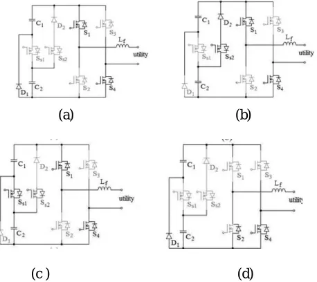
sinusoidal and in phase with the utility voltage, the output current of the seven-level inverter is also positive in the positive half cycle of the utility. The operation of the seven-level inverter in the positive half cycle of the utility can be further divided into four modes, as shown in Fig 3.
(a) (b)
(c ) (d)
Fig 4 Operation of the seven-level inverter in the positive half cycle, (a) Mode 1, (b) mode 2, (c) mode 3, and (d) mode 4.
Mode 1: The operation of mode 1 is shown in Fig 4(a). BothSS1 andSS2 of the capacitor selection circuit are OFF,
soC1 is discharged through D1 and the output voltage of the capacitor selection circuit is Vdc/3.S1andS4of the
full-bridge power converters are ON. At this point, the output voltage of the seven-level inverter is directly equal to the output voltage of the capacitor selection circuit, which means the output voltage of the seven-level inverter is Vdc/3.
Mode 2: The operation of mode 2 is shown in Fig 4(b). Inthe capacitor selection circuit,SS1is OFF and SS2is ON,
soC2 is discharged throughSS2andD2and the output voltage of the capacitor selection circuit is 2Vdc/3.S1andS4of the full-bridge power converter are ON. At this point, the output voltage of the seven-level inverter is 2Vdc/3.
Mode 3: The operation of mode 3 is shown in Fig 4(c). Inthe capacitor selection circuit, SS1 is ON. Since D2 has a
circuit is Vdc. S1 andS4 of the full-bridge power converter are ON. At this point, the output voltage of the seven-level
inverter is Vdc.
Mode 4: The operation of mode 4 is shown in Fig 4(d).BothSS1 and SS2 of the capacitor selection circuit are OFF.
The output voltage of the capacitor selection circuit is Vdc/3. OnlyS4 of the full-bridge power converter is ON. Since the output current of the seven-level inverter is positive and passes through the filter inductor, it forces the anti parallel diode of S2 to be switched ON for continuous conduction of the filter inductor current. At this point, the output voltage of the seven level inverter is zero. Therefore, in the positive half cycle, the output voltage of the seven-level inverter has four levels:Vdc,2Vdc/3,Vdc/3, and 0.
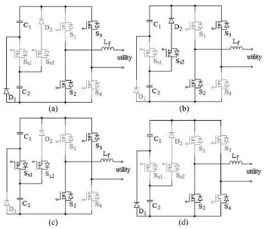
In the negative half cycle, the output current of the seven-level inverter is negative. The operation of the seven-level inverter can also be further divided into four modes, as shown in Fig 5. A comparison with Fig 4 shows that the operation of the capacitor selection circuit in the negative half cycle is the same as that in the positive half cycle. The difference is that S2 andS3 of the full-bridge power converter are ON during modes 5, 6, and 7, andS2 is also ON during mode 8 of the negative half cycle. Accordingly, the output voltage of the capacitor selection circuit is inverted by the full-bridge power converter, so the output voltage of the seven-level inverter also has four levels: −Vdc,
−2Vdc/3,−Vdc/3, and 0. In summary, the output voltage of the seven-level inverter has the voltage
levels:Vdc,2Vdc/3,Vdc/3, 0,−Vdc/3,−2Vdc/3, and −Vdc. The seven-level inverter is controlled by the current-mode control, and pulse-width modulation (PWM) is use to generate the control signals for the power electronic switches. The output voltage of the seven-level inverter must be switched in two levels, according to the utility voltage. One level of the output voltage is higher than the utility voltage in order to increase the filter inductor current, and the other level of the output voltage is lower than the utility voltage, in order to decrease the filter inductor current. In this way, the output current of the seven-level inverter can be controlled to trace a reference current.
Fig 5 Operation of the seven-level inverter in the negative half cycle: (a) Mode 5, (b) mode 6, (c) mode 7, and (d) mode 8.
Accordingly, the output voltage of the seven-level inverter must be changed in accordance with the utility voltage. In the positive half cycle, when the utility voltage is smaller than Vdc/3, the seven-level inverter must be
switched between modes 1 and 4 to output a voltage of Vdc/3 or 0. Within this voltage range, S1 is switched in PWM. The duty ratio d of S1 can be represented as
(3)
Where Vm and Vtri are the modulation signal and the amplitude of carrier signal in the PWM circuit,
respectively. The output voltage of the seven-level inverter can be written as
(5)
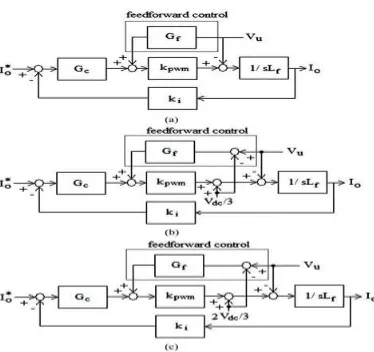
Fig .5(a) shows the simplified model for the seven-level inverter when the utility voltage is smaller than Vdc/3. The closed loop transfer function can be derived as
(6) Where Gc is the current inverter and ki is the gain of the current detector. The seven-level inverter is switched between modes 2 and 1, in order to output a voltage of 2Vdc/3 or Vdc/3 when the utility voltage is in the range (Vdc/3, 2Vdc/3). Within this voltage range, SS2 is switched in PWM. The duty ratio ofSS2 is the same as
(3). However, the output voltage of seven-level inverter can be written as
(7)
Fig 6. Model of the seven-level inverter under different range of utility voltage, (a) in the range of smaller than Vdc/3, (b) in the range of (Vdc/3, 2Vdc/3), (c) in the range of higher than 2Vdc/3
Fig 6(b) shows the simplified model for the seven-level inverter when the utility voltage is within this voltage range. The closed-loop transfer function can be derived as
(8) The seven-level inverter is switched between modes 3 and 2 in order to output a voltage of Vdc or 2Vdc/3, when the utility voltage is in the range (2Vdc/3, Vdc). Within this voltage range, SS1 is switched in PWM and SS2 remains in the ON state to avoid switching ofSS2. The duty ratio of SS1 is the same as (3). However, the output voltage of seven-level inverter can be written as
(10)
TABLE I
STATES OF POWER ELECTRONIC SWITCHES FOR ASEVEN- LEVEL INVERTER
As seen in (6), (8), and (10), the second term is the disturbance. Hence, a feed forward control, which is also shown in Fig5, should be used to eliminate the disturbance, and the gain Gf should be 1/kpwm. In the negative half cycle, the seven-level inverter is switched between modes 5 and 8, in order to output a voltage of−Vdc/3 or 0, when the absolute value of the utility voltage is smaller than Vdc/3. Accordingly, S3 is switched in PWM. The seven level inverter is switched in modes 6 and 5 to output a voltage of−2Vdc/3 or −Vdc/3 when the utility voltage is in the range (−Vdc/3, −2Vdc/3).Within this voltage range, SS2 is switched in
PWM. The seven-level inverter is switched in modes 7 and 6 to output a voltage of−Vdc or−2Vdc/3, when the utility voltage is in the range (−2Vdc/3, −Vdc). At this voltage range, SS1 is switched in PWM and SS2 remains in the ON state to avoid switching ofSS2. The simplified model for the seven-level inverter in the negative half cycle is the similar to that for the positive half cycle. Since only six power electronic switches are used in the proposed seven-level inverter, the power circuit is significantly simplified compared with a conventional seven-level inverter. The states of the power electronic switches of the seven-level inverter, as detailed previously, are summarized in Table I. It can be seen that only one power electronic switch is switched in PWM within each voltage range and the change in the output voltage of the seven-level inverter for each switching operation is Vdc/3, so switching power loss is reduced. Figs 3 and 4 show that only three semiconductor devices are conducting in series in modes 1, 3, 4, 5, 7, and 8 and four semiconductor devices are conducting in series in modes 2 and 6. This is superior to the conventional multi-level inverter topologies, in which at least four semiconductor devices are conducting in series. Therefore, the conduction loss of the proposed seven-level inverter is also reduced slightly. The drawback of the proposed seven-level inverter is that the voltage rating of the full-bridge converter is higher than that of conventional multilevel inverter topologies. The leakage current is an important parameter in a solar power generation system for transformer less operation. The leakage current is dependent on the parasitic capacitance and the negative terminal voltage of the solar cell array respect to ground. To reduce the leakage current, the filter inductor Lf should be replaced by a symmetric topology and the
A. SEVEN-LEVEL INVERTER
Fig.7(a) shows the control block diagram for the seven-level inverter. The control object of the seven-level inverter is its output current, which should be sinusoidal and in phase with the utility voltage. The utility voltage is detected by a voltage detector, and then sent to a phase-lock loop (PLL) circuit in order to generate a sinusoidal signal with unity amplitude. The voltage of capacitor C2 is detected and then compared with a setting voltage. The compared result is sent to a PI inverter. Then, the outputs of the PLL circuit and the PI inverter are sent to a multiplier to produce the reference signal, while the output current of the seven-level inverter is detected by a current detector. The reference signal and the detected output current are sent to absolute circuits and then sent to subtract or, and the output of the subtract or is sent to a current inverter. The detected utility voltage is also sent to an absolute circuit and then sent to a comparator circuit, where the absolute utility voltage is compared with both half and whole of the detected voltage of capacitor C2, in order to determine the range of the operating voltage. The comparator circuit has three output signals, which correspond to the operation voltage ranges, (0, Vdc/3), (Vdc/3, 2Vdc/3), and (2Vdc/3, Vdc). The feed-forward control eliminates the disturbances of the utility voltage, Vdc/3 and 2Vdc/3, as shown in (6), (8), and (10). The absolute value of the utility voltage and the outputs of the compared circuit are sent to a feed-forward inverter to generate the feed-forward signal. Then, the output of the current inverter and the feed-forward signal are summed and sent to a PWM circuit to produce the PWM signal. The detected utility voltage is also compared with zero, in order to obtain a square signal that is synchronized with the utility voltage. Finally, the PWM signal, the square signal, and the outputs of the compared circuit are sent to the switching signal processing circuit to generate the control signals for the power electronic switches of the seven-level inverter, according to Table I. The current inverter controls the output current of the seven level inverter, which is a sinusoidal signal of 60 Hz. Since the feed-forward control is used in the control circuit, the current inverter can be a simple amplifier, which gives good tracking performance. As can be seen in (6), (8), and (10), the gain of the current inverter determines the bandwidth and the steady state error. The gain of the current inverter must be as large as possible in order to ensure a fast response and a low steady-state error. But the gain of the current inverter is limited because the bandwidth of the power converter is limited by the switching frequency.
B. DC–DC POWER CONVERTER
VI. MATALAB/SIMULINK RESULTS
Case I. Seven level inverter for RES by using PI inverter
Fig.8.Simulink circuit for proposed seven level inverter using PI Inverter.
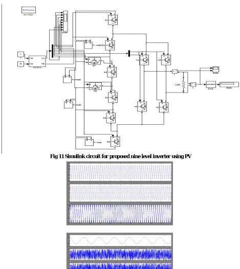
Fig 11 Simulink circuit for proposed nine level inverter using PV
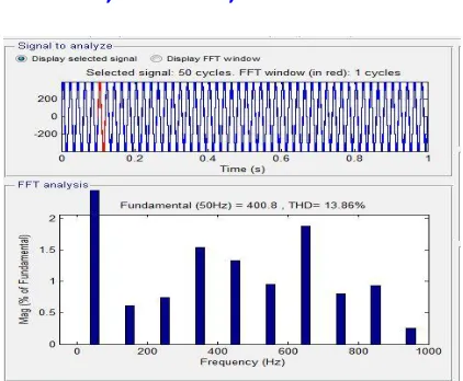
Fig 14 FFT analysis for inverter current
VII. CONCLUSION
The proposed technique has some features such as it reduces the cost of the overall system, compact size as well as an increased efficiency. With the help of lower number of switches, seven-level of output voltages are generated and thus it reduces the switching loss and conduction losses. The THD of seven-level inverter This paper proposes a solar power generation system to convert the dc energy generated by a solar cell array into ac energy that is fed into the utility. The proposed solar power generation system is composed of a dc–dc power converter and a nine level inverter. The nine-level inverter contains less power electronic switches, which simplifies the circuit configuration. This reduces the switching power loss and improvesthepowerefficiency. Experimental results show that the proposed solar power generation system generates a nine-level output voltage and outputs a sinusoidal current that is in phase with the utility voltage, yielding a power factor of unity. In addition, the proposed solar power generation system can effectively trace the maximum power of solar cell array.
REFERENCES
[1] Jinn-Chang Wu, Member, IEEE, and Chia-Wei Chou, ―A Solar Power Generation System With a Seven-Level Inverter,‖ IEEE Trans. Power Electron., vol. 29,no. 7,
pp. 3454–3462, July. 2014. [2] Fan Zhang, Kary Thanapalan, Andrew Procter, Stephen Carr, and Jon Maddy, ―Adaptive Hybrid Maximum Power Point Tracking Method for a Photovoltaic System‖ IEEE Trans. Energy Conversion, vol. 28, no. 2, pp.353-360, June. 2013.
[3] J. D. Barros, J. F. A. Silva, and E.G.A Jesus, ―Fast-predictive optimal control of NPC multilevel converters,‖ IEEE Trans. Ind. Electron., vol. 60, no. 2, pp. 619–627, Feb. 2013.
[4] J. Chavarria, D. Biel, F. Guinjoan, C.Meza, and J. J. Negroni, ―Energy balance control of PV cascaded multilevel grid-connected inverters under level-shifted and phase-shifted PWMs,‖ IEEE Trans. . Electron., vol. 60, no. 1, pp. 98–111, Jan. 2013.
[5] X. She, A. Q. Huang, T. Zhao, and G. Wang, ―Coupling effect reduction of a voltage-balancing inverter in single-phase cascaded multilevel converters,‖ IEEE
Trans. Power Electron., vol. 27, no. 8, pp. 3530–3543, Aug. 2012.
[6] S. Choi and M. Saeedifard, ―Capacitor voltage balancing of
flying capacitor multilevel converters by space vector PWM,‖ IEEE Trans. Power Delivery, vol. 27, no. 3, pp. 1154–1161, Jul. 2012.
[7] R. A. Mastromauro, M. Liserre, and A. Dell‘ Aquila, ―Control issues in single-stage photovoltaic systems: MPPT, current and voltage control,‖ IEEE Trans. Ind.
Informat., vol. 8, no. 2, pp. 241–254, May. 2012.
[8] L. Maharjan, T. Yamagishi, and H. Akagi, ―Active-power control of individual converter cells for a battery energy storage system based on a multilevel cascade PWM converter,‖ IEEE Trans. Power Electron., vol. 27, no. 3, pp. 1099–1107, Mar. 2012.
BIOGRAPHY
Mr. K.SRINIVASULU he is pursuing M.Tech at Dr.samuel George institute of engineering &technology.Markapur,Jntu Kakinada University.