N A N O E X P R E S S
Open Access
Metal work-function-dependent barrier height of
Ni contacts with metal-embedded nanoparticles
to 4H-SiC
Min-Seok Kang
1†, Jung-Joon Ahn
1†, Kyoung-Sook Moon
2†and Sang-Mo Koo
1*†Abstract
Metal, typically gold [Au], nanoparticles [NPs] embedded in a capping metal contact layer onto silicon carbide [SiC] are considered to have practical applications in changing the barrier height of the original contacts. Here, we demonstrate the use of silver [Ag] NPs to effectively lower the barrier height of the electrical contacts to 4H-SiC. It has been shown that the barrier height of the fabricated SiC diode structures (Ni with embedded Ag-NPs) has significantly reduced by 0.11 eV and 0.18 eV with respect to the samples with Au-NPs and the reference samples, respectively. The experimental results have also been compared with both an analytic model based on Tung’s theory and physics-based two-dimensional numerical simulations.
Introduction
Recently, silicon carbide [SiC] has been proposed as the material of choice especially for power electronic and sen-sing devices operating under high temperature, fast switching, and high-power conditions mainly due to its wide bandgap (3.26 eV), high critical electric field (2.2 × 10⁶V/cm), superior thermal conductivity (4.9 W/Kcm), and high bulk electron mobility (900 cm2/Vs) of the 4H polytype [1,2]. For stable operations at high power densi-ties and elevated temperatures, SiC diodes, including Schottky barrier diodes and junction barrier Schottky diodes, as well as SiC transistors, have been under exten-sive exploration with great improvements in wafer growth technology and device process.
In order to realize stable SiC devices, metal contacts to SiC with suitable physical and electrical characteristics are required. For example, Ohmic contacts with low contact resistances and Schottky contacts with controlled barrier height (FB) between SiC and metal are among the most important factors for determining the performance of SiC devices [3-5]. Furthermore, electrical characteristics of devices, such as voltage drop and switching speed of such devices, are dependent on the current transport behavior
through the structure of the metal/4H-SiC interface. It is, therefore, of critical importance to reduce the barrier height of the metal/4H-SiC interface in order to improve the on-state voltage drop in 4H-SiC devices.
To date, extensive studies have been carried out on the properties of barrier height of various metals on n- and p-types for SiC [6,7], and many attempts have been made to modify the contact barrier height on SiC. The effect of inhomogeneities and Fermi-level pinning on Schottky con-tact properties has been known to be minimal, and the barrier height depends mostly on the metal work function without strong Fermi-level pinning for SiC [4,5]. Recent work on the electrical contacts to SiC includes the imple-mentation of nanostructures such as metal nanoparticles [NPs] to modify the barrier height at metal-SiC interfaces and to alter fundamental SiC device properties by control-ling the size of the metal NPs. Previous results in the lit-erature have been primarily focused on the effect of size reduction of NPs on the characteristics of diode structures with embedded NPs, which experimentally investigates the change in transport properties of metal/semiconductor interfaces in SiC depending on the size of NPs [5-10]. However, so far, the focus has been mainly on the scaling effect of the NPs rather than on altering the electrical bar-rier of the NPs.
In this work, we demonstrate that the work function change in the embedded metal NPs can effectively control the barrier height change of the SiC diode structures. Our
* Correspondence: [email protected] †Contributed equally
1
Department of Electronic Materials Engineering, Kwangwoon University, 447-1 Wolgye-dong, Nowon-gu, Seoul, 139-701, South Korea
Full list of author information is available at the end of the article
results show that incorporating NPs with a larger work function difference to the capping metal layer results in an improved barrier lowering by further enhancing the local electric field. The experimental results have also been compared with both an analytic model based on Tung’s theory [11-13] and physics-based two-dimensional numer-ical simulations.
Experimental details
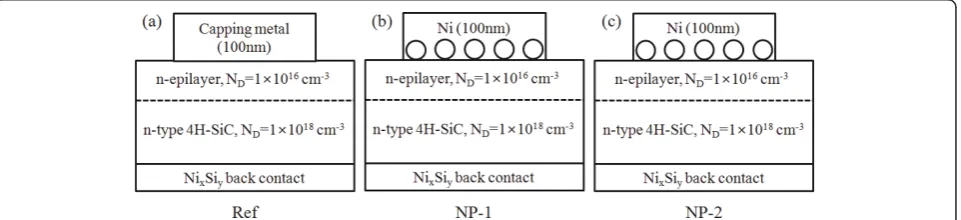
The starting materials are n-type 4H-SiC wafers with an 8-μm-thick n-type epilayer (ND= 1 × 1016cm-3) grown on an n+ substrate (ND= 1 × 1019cm-3). A large area Ohmic contact on the back was formed by e-beam evaporation of a 100-nm-thick Ni film, followed by a rapid thermal annealing process at 950°C in N2for 90 s [14]. After the samples were cleaned in H2SO4:H2O2 = 4:1, the native oxide was removed by a BOE dip. A thin layer (10 nm) of metal film (Au and Ag, respectively) was then deposited on the front side of the samples by e-beam evaporation, and the samples were annealed in a quartz tube furnace at 500°C for 20 min to induce the formation and growth of the metal NPs [15,16]. As a capping layer, a 100-nm-thick Ni film was deposited on the front side of the samples to form macroscopic circular patterns with an area of 3.14 × 10⁻²cm2. We then obtained macroscopic Ni/SiC diodes with embedded NPs with different metal work function values from the capping metal/4H-SiC interface. Note that the bulk work function differences along Au and Ni-Ag areΔFB(Ni-Au)which is 0.21 eV andΔFB(Ni-Ag)which is 0.84 eV, respectively [17,18]. The device structures stu-died in this work are basically Ni/SiC contacts embedded with the metal NPs to the 4H-SiC substrate. Figure 1 shows the fabricated samples with metal NPs: Ni/SiC tacts embedded with the Au-NPs (NP-1) and Ni/SiC con-tacts embedded with the Ag-NPs (NP-2). Note that control samples (Ref) were also prepared for comparison by sputtering a 100-nm-thick Ni directly onto the SiC sub-strate without the NPs. Table 1 summarizes all the differ-ent sets of fabricated samples and process conditions.
The barrier height and ideality factor were compared with the physical distribution condition of the NPs as
determined by field emission scanning electron micro-scopy [FE-SEM]. To investigate the effect of the NPs at the Ni/SiC interface on the electrical properties, cur-rent-voltage [I-V] and capacitance-voltage [C-V] charac-teristics of the devices were measured by using a Keithley 4200 semiconductor parameter analyzer (Keith-ley Instruments Inc., Cleveland, OH, USA). The experi-mental results have also been compared with an analytic model based on Tung’s theory [11-13] and further veri-fied by considering band diagram and electric field dis-tribution using a physics-based two-dimensional numerical simulator Atlas (Silvaco Inc., Santa Clara, CA, USA) [19].
[image:2.595.304.538.111.172.2]Results and discussion
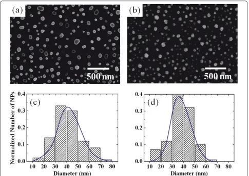
Figure 2a, b shows representative FE-SEM surface images of the nanoscale metal particles formed on SiC, where Au (NP-1) and Ag (NP-2) particles were formed after annealing 10-nm thick, corresponding metal films depos-ited on (0001) 4H-SiC at 500°C. It is clear that the metal (Au and Ag) films were fully agglomerated after anneal-ing for 20 min. The physical distribution condition of the NPs has been determined by the SEM images. Figure 2c, d shows the distribution of relative amounts of the NPs in the samples sorted according to size. The diameter dis-tribution in the samples was fitted by a Gaussian distri-bution and shown in a blue line in each histogram, where the peak position was taken as the average diameter (< 2R>), with a standard deviation [s]. The average dia-meters of the Au and Ag NPs were 40.5 nm with asof 11.7 nm and 36.1 nm with asof 10.3 nm, respectively. It is noticeable in Figure 2 that the difference of the NPs’
Figure 1Schematic view of Ni contacts with embedded nanoparticles on SiC. (a) Ni/SiC contacts without NPs (Ref), (b) Ni/SiC contacts embedded with the Au-NPs (NP-1), and (c) Ni/SiC contacts embedded with the Ag-NPs (NP-2).
Table 1 Summary of all the different sets of fabricated samples and process conditions
Sample NPs Capping layer
< 2R> (nm) s(nm)
NP Annealing
Ref - Ni - -
-NP-1 Au Ni 40.5 11.7 500°C, 20 min NP-2 Ag Ni 36.1 10.3 500°C, 20 min Kanget al.Nanoscale Research Letters2012,7:75
http://www.nanoscalereslett.com/content/7/1/75
[image:2.595.60.541.593.703.2]sizes compared to the NP-1 sample and NP-2 sample was rather small (below 6%).
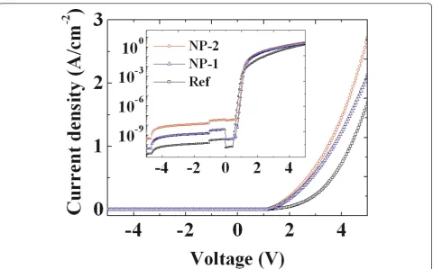
Figure 3 shows the current density-voltage [J-V] char-acteristics of the as-deposited Ni contacts and samples
with different embedded NPs. FromI-V measurements,
the saturation current density, effective ideality factor, and effective barrier height can be extracted in a plot of ln (J)-V characteristics. According to the thermionic emission model, the J-V characteristics are given by [20,21] the following equations:
J=Jsexp
qV
nkT 1−exp
qV kT
(1)
Js=A∗T2exp
−qΦB
kT
, (2)
where Js is the saturation current density, FBis the effective barrier height [FB=kT/eln(A*T2/Js)],A* is the Richard constant (for 4H-SiC, 146 A/cm2 K2) [22], Tis
the absolute temperature,kis the Boltzman constant, q
is the electron charge, and nis the ideality factor [n = kT/e(dV/d(lnJ))]. The values of the effective ideality fac-tor and barrier height were calculated from the ln (J) versus forward voltageVcharacteristics. Under forward voltage conditions, it clearly shows that the current value of sample NP-2 was about one order of magnitude higher than that of reference samples (10-3 A/cm2), due to the smaller barrier height of NP-2 (0.87 eV) com-pared with that of Ref (1.04 eV).
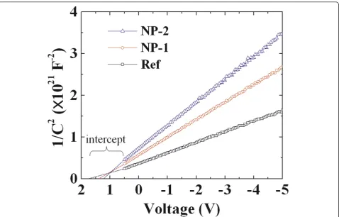
The barrier height from C-V measurements was
extracted as well for comparison with theI-V measure-ments. The doping concentration (ND) of the epilayers can be determined from the slope in plotting 1/C2versus the reverse voltage, which can be expressed as follows [23]:
ND=
2
qKSε0A2
d1/C2 dV
,
[image:3.595.70.217.614.681.2](3)
where,Ais the contact area of the diode (3.14 × 10⁻² cm2), KS is the semiconductor dielectric constant for 4H-SiC (6.52 at high frequency), andε0is the permittiv-ity free space charge. Figure 4 shows the 1/C2 versus reverse voltage characteristics measured at a frequency of 1 MHz at room temperature. The straight line inter-cepts of the 1/C2-Vcharacteristics with voltage axis are obtained, and thus, the barrier height values can be given as follows [23]:
ΦB=Vi+Vn, (4)
whereViis the voltage intercept,Vnis the energy dif-ference between the minimum of the conduction band and Fermi level in the bulk of n-type SiC [Vn=kT/eln (NC/ND)], and NC is the conduction band density of states for 4H-SiC at 300 K (approximately 1.66 × 1019 cm-3) [24]. As observed from both I-V and C-V mea-surement results, all the samples exhibit excellent recti-fying behavior with stable ideality factors.
Figure 5a shows the relative barrier height difference between the samples with NPs (NP-1 and NP-2) and the reference samples, respectively, which are extracted fromI-Vand C-Vmeasurements. There is some quanti-tative difference between the extracted values from the two different measurements; the extracted values for the
barrier heights for the reference sample and the ideality factor are FB(I-V)which is 1.04 eV andFB(C-V)which is 1.69 eV, respectively, withnat 1.50 for the control sam-ples. The difference from the two different methods is commonly observed, which normally shows higher values forC-Vmeasurements than those obtained from
I-V characteristics due to additional capacitance at the interface [3,25].
The results, however, clearly suggest that the barrier height difference between the Ni/SiC contacts (Ref) and samples with embedded NPs significantly increases and that the enhancement becomes greater for Ag particles (NP-2) than for Au particles (NP-1). The values of barrier height lowering are 0.06 eV and 0.07 eV for NP-1, whereas the values are clearly increased to 0.17 eV and 0.18 eV for NP-2 as obtained fromI-VandC-V measure-ments, respectively. Note that the reduced barrier height and improved ideality factor are attributed to the the lar-ger difference in the metal work function of Ag than that of Au with respect to the capping metal of Ni.
[image:4.595.59.540.86.385.2]In order to understand this reduction of the barrier height, we have used an analytic model by Tung [13,14], which considers the current transport theory at the metal/semiconductor interfaces with inhomogeneous barrier height [16]. In general, conventional theories of
Figure 3I-Vcharacteristics of Ni films. The current-voltage characteristics of Ni film without NPs (Ref), Ni film with embedded Au-NPs (NP-1), and Ni film with embedded Ag-NPs (NP-2) to n-type 4H-SiC.
Kanget al.Nanoscale Research Letters2012,7:75 http://www.nanoscalereslett.com/content/7/1/75
current transport, such as the thermionic emission and diffusion, are inadquate for effectively considering improved electrical behaviors associated with the NPs. The electric field E for the circular patch geometry of NPs at the depletion region close to the surface of the semiconductor is given by the following equation [6,13]:
E(z) =Vbi
2
w−
2z w2
−Φ ⎡ ⎢
⎣ 1
z2+R 02
− z2 (z2+R
02)3 ⎤ ⎥
⎦, (5)
wherez is the distance from the surface of the semi-conductor, wis the depletion width, R0 is the radius of the circular patch, andΔF is the difference of the bar-rier height between the capping metal and NPs.
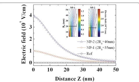
Figure 6 shows the calculated electric field distribution as a function of the depth from the surface of the NPs using Equation 5. The presence of small regions with a low barrier height,FB- Δ, due to the difference of the barrier height between the capping metal (Ni) and NPs results in the increased electric field at the depletion region close to the surface of the semiconductor. As shown in Figure 6, the values of the electric field are
estimated to be 2.6 × 10⁴ V/cm (Ref), 0.1 × 10⁷ V/cm (NP-1), and 3.9 × 10⁷ V/cm (NP-2) for the given experi-mental conditions including the diameters of the NPs, namely, 2R0which is 40 nm for NP-1 and 2R0 which is 35 nm for NP-2. The insets of Figure 6 show the electric field distribution as a function of the size of the NPs at n-type 4H-SiC. The electric field is increased as the small size of the NPs decreases due to the increased dif-ference of the barrier height between Ni and the NPs. The electric field at the surface of sample NP-2 is there-fore higher than that of NP-1 for a similar particle diameter.
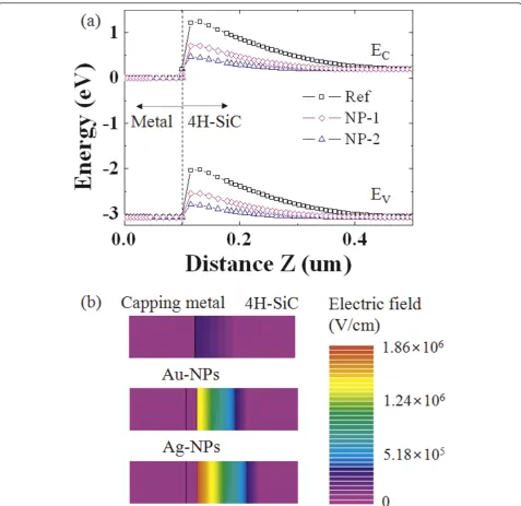
[image:5.595.60.539.87.393.2]To further examine this effect and understand the trans-port properties, we have performed two-dimensional numerical simulations. Figure 7a, b shows the electric field distribution of the metal-SiC structure, and it indicates that the maximum electric field is at the depletion region close to the surface of SiC and corresponding energy band profiles. The maximum electric field is increased up to 1.8 × 10⁶and 2.4 × 10⁶for NP-1 and NP-2, respectively, compared to the value of 5.18 × 10⁵for Ref. The increased electric field of the samples with the Au and Ag NPs is
mainly attributed to the reduction of barrier height as the effective barrier of the conduction band at the depletion region decreases. As shown in Figure 7a, the extracted energy band diagram profiles along the cut line across the NP-substrate structures show that the reduction of barrier is more profound in NP-2 (with Ag) than in NP-1.
Conclusions
[image:6.595.58.290.88.368.2]In summary, we demostrate that the work function change in the embedded metal NPs can effectively lower the barrier height of the SiC diode structures. It has been experimentally shown that incorporating NPs (Ag) with a larger work function difference to the cap-ping metal layer (Ni) results in an improved barrier lowering by further enhancing the local electric field. The barrier height of the fabricated SiC diode structures (NP-1; Ni with embedded Ag-NPs) has significantly reduced by 0.11 eV and 0.18 eV with respect to the samples with Au-NPs (NP-2) and the reference samples, respectively. The experimental results are in agreement with both analytic calulations based on Tung’s model and physics-based two-dimensional numerical simula-tions, which confirm that the increased electric field of the samples with NPs is mainly attributed to the reduc-tion of barrier height as the effective barrier of the con-duction band at the depletion region of the surface decreases.
Figure 5Barrier height difference and ideality factor. (a) Barrier height difference between the samples with NPs (NP-1 and NP-2) and the reference sample usingI-VandC-Vcharacteristics. (b) Ideality factor of fabricated diodes extracted fromI-Vcharacteristics.
Figure 6Electric field distribution. Comparison of the electric field distribution at the depletion region close to the surface of the 4H-SiC of different work functions using Tung’s model. The inset represents the electric field distribution as a function of the size of the NPs.
Kanget al.Nanoscale Research Letters2012,7:75 http://www.nanoscalereslett.com/content/7/1/75
[image:6.595.59.538.421.703.2]Acknowledgements
This work was supported by the National Research Foundation Grants 2011-0017942 and 2011-0003298 through a research grant from Kwangwoon University in 2011, and Korea-Sweden Collaboration Project.
Author details
1Department of Electronic Materials Engineering, Kwangwoon University,
447-1 Wolgye-dong, Nowon-gu, Seoul, 139-701, South Korea2Department of
Mathematics and Information, Kyungwon Campus, Gachon University, Seongnam, 461-701, South Korea
Authors’contributions
MSK carried out the experiments and characterization and prepared the manuscript initially. JJA participated in the experiments on nanoparticle formation. KSM participated in the discussion of the analytical model and
carried out the numerical calculation. SMK conceived the study and participated in its design and coordination.
All authors read and approved the final manuscript.
Competing interests
The authors declare that they have no competing interests.
Received: 15 July 2011 Accepted: 13 January 2012 Published: 13 January 2012
References
[image:7.595.59.537.87.550.2]1. Liu X, Luo Z, Han S, Tang T, Zhang D, Zhou C:Band engineering of carbon nanotube field-effect transistors via selected area chemical gating.Appl Phys Lett2005,86:243501-243503.
2. Guy OJ, Lodzinski M, Teng KS, Maffeis TGG, Tan M, Blackwood I, Dunstan PR, Al-Hartony O, Wilks SP, Wilby T, Rimmer N, Lewis D, Hopkins J: Investigation of the 4H-SiC surface.Appl Surf Sci2008,254:8098-8105. 3. Itoh A, Matsunami H:Analysis of Schottky barrier heights of metal/SiC
contacts and its possible application to high-voltage rectifying devices.
Phys Stat Sol1997,162:389-408.
4. Porter LM, Davis RF:Critical review of ohmic and rectifying contacts for silicon carbide.Mater Sci Eng1995,34:83-105.
5. Sohn JI, Song JO, Leem DS, Lee SH:Nano-dot addition effect on the electrical properties of Ni contacts to p-type GaN.Phys Stat Sol2004, 10:2524-2527.
6. Lee SK, Zetterling CM, Östling M, Åberg I, Magnusson MH, Deppert K, Wernersson LE, Samuelson L, Litwin A:Reduction of the Schottky barrier height on silicon carbide using Au nano-particles.Solid State Electron
2002,46:1443-1440.
7. Ruffino F, Crupi I, Irrera A, Grimaldi MG:Pd/Au/SiC nanostructured diodes for nanoelectronics: room temperature electrical properties.IEEE Trans Nanotechnology2010,9:414-421.
8. Langhuth H, Frédérick S, Kaniber M, Finley J, Rührmair U:Strong photoluminescence enhancement from colloidal quantum dot near silver nano-island films.J Fluoresc2011,21:539-543.
9. Iucolano F, Roccaforte F, Giannazzo F, Raineri V:Temperature behavior of inhomogeneous Pt/GaN Schottky contacts.J Appl Phys2007,102:092119. 10. Fadwa J, Nilanthi W, Philippe B, Frédéric V, Sarah YS, Gilles T, Michael A,
Pierre D, Maïté CM, Marie A, Michel G:3D exploration of light scattering from live cells in the presence of gold nanomarkers using holographic microscopy.3D Res2011,02:01002.
11. Tung RT:Electron transport at metal-semiconductor interfaces: general theory.Phys Rev B1992,45:13509-13523.
12. Tung RT:Electron transport of inhomogeneous Schottky barriers.Appl Phys Lett1991,58:2821-2823.
13. Sullivan JP, Tung RT, Pinto MR:Electron transport of inhomogeneous Schottky barriers: a numerical study.J Appl Phys1991,70:7403-7424. 14. Huang YP, Chen CW, Shen TC, Huang JF:Autostereoscopic 3D display
with scanning multi-electrode driven liquid crystal (MeD-LC) lens.3D Res
2010,01:39-42.
15. Kwon JY, Yoon TS, Kim KB:Comparison of the agglomeration behavior of Au and Cu films sputter deposited on silicon dioxide.J Appl Phys2003, 93:3270-3278.
16. Spadavecchia J, Prete P, Lovergine N, Tapfer L, Rella P:Au nanoparticles prepared by physical method on Si and sapphire substrates for biosensor applications.J Phys Chem B2005,109:17347-17349.
17. Clemenger K:Spherical supershells in metal clusters and the transition to protocrystalline structure.Phys Rev B1991,44:12991-13001.
18. Chiang KC, Cheng CH, Jhou KY, Pan HC, Hsiao CN, Chou CP, McAlister SP, Hwang HL:Use of a high-work-function Ni electrode to improve the stress reliability of analog SrTiO3metal-insulator-metal capacitors.IEEE
Trans Electron Devices2007,28:694-696.
19. Silvaco International:Atlas User’s ManualSanta Clara. CA; 1998. 20. Rhoderick EH, Williams RH: InMetal-Semiconductor Contacts. Volume 19..2
edition. Oxford: Clarendon Press; 1988.
21. Sze SM:Physics of Semiconductor Devices.2 edition. New York: John Wiley & Sons; 1981.
22. Pirri CF, Ferrero S, Scaltrito L, Perrone D, Guastella S, Furno M, Richieri G, Merlin L:Intrinsic 4H-SiC parameters study by temperature behaviour analysis of Schottky diodes.Microelectron Eng2006,83:86-88.
23. Neamen DA:Semiconductor Physics and Devices.3 edition. Boston: McGraw-Hill; 2003.
24. Bakowski M, Gustafsson U, Lindefelt U:Simulation of SiC high power devices.Phys Stat Sol1981,162:421-440.
25. Osvald J:Numerical study of electrical transport in inhomogeneous Schottky diodes.J Appl Phys1999,85:1935-1942.
doi:10.1186/1556-276X-7-75
Cite this article as:Kanget al.:Metal work-function-dependent barrier height of Ni contacts with metal-embedded nanoparticles to 4H-SiC.
Nanoscale Research Letters20127:75.
Submit your manuscript to a
journal and benefi t from:
7Convenient online submission
7Rigorous peer review
7Immediate publication on acceptance
7Open access: articles freely available online
7High visibility within the fi eld
7Retaining the copyright to your article
Submit your next manuscript at 7 springeropen.com
Kanget al.Nanoscale Research Letters2012,7:75 http://www.nanoscalereslett.com/content/7/1/75