N A N O E X P R E S S
Open Access
Quantum dot cascade laser
Ning Zhuo, Feng Qi Liu
*, Jin Chuan Zhang, Li Jun Wang, Jun Qi Liu, Shen Qiang Zhai and Zhan Guo Wang
Abstract
We demonstrated an unambiguous quantum dot cascade laser based on InGaAs/GaAs/InAs/InAlAs heterostructure by making use of self-assembled quantum dots in the Stranski-Krastanow growth mode and two-step strain compensation active region design. The prototype generates stimulated emission atλ~ 6.15μm and a broad electroluminescence band with full width at half maximum over 3μm. The characteristic temperature for the threshold current density within the temperature range of 82 to 162 K is up to 400 K. Moreover, our materials show the strong perpendicular mid-infrared response at about 1,900 cm−1. These results are very promising for extending the present laser concept to terahertz quantum cascade laser, which would lead to room temperature operation.
Keywords:Quantum dot; Quantum cascade laser; MBE; Mid-infrared PACS:42.55.Px; 78.55.Cr; 78.67.Hc
Background
Quantum cascade lasers are semiconductor laser sources based on intersubband transitions in multiple quantum well systems [1]. Their unique operation principle and good performance have established themselves as the leading tunable coherent semiconductor source in the infrared and terahertz ranges of the electromagnetic spectrum [2-10]. Although quantum cascade lasers have experienced rapid development, several drawbacks still exist. First of all, the intersubbands transition nature leads to relatively narrow gain spectrum and, conse-quently, narrow spectrum tunability [11]. Moreover, due to intersubband selection rules, the emitting light is po-larized in the growth direction, which makes surface emission impossible. Another drawback is that due to numerous in-plane scattering paths that the electrons undergo and decrease the upper lasing state lifetime, the threshold current is increased and the wall plug effi-ciency is decreased [12-17]. An appealing and ambitious route to tackle these difficulties is to explore quantum dot cascade laser (QDCL) [17,18], by substituting the quantum wells (QWs) in the active region with self-assembled quantum dots (QDs).
The development of QDCL using self-assembled QDs as substitute for QWs in the active region faces two
challenges: (1) the QDs' size and controllability, implying the effective of three-dimensional (3D) quantum con-finements, i.e., the prerequisite of realizing the ‘phonon bottleneck’ effect and (2) the adjustable energy levels, which satisfy critical requirements of injection and extrac-tion efficiency. Here, our design targets precisely these challenges: first, two-step strain compensation mechanics using InGaAs/GaAs/InAs/InAlAs material system can realize controllable InAs QDs on tensile-strained InAlAs layers; second, the population inversion is achieved be-tween lower levels of coupled InAs QDs and upper hybrid QW-dominated lasing states.
Methods
Considering that InAs QDs grown on GaAs/AlGaAs ma-terial system [19-21] lack of a suitable extraction mechan-ism from the levels confined in the QDs and InAs QDs grown on InP-based InGaAs/InAlAs material system [22-27] tend to be quantum dashes due to lower strain and the influence of embedding material, the radical way to realizing controllable InAs QDs in the active region is illustrated in Figure 1.
Figure 1 depicts the growth mechanics of coupled InAs QDs in the QDCL wafer. In order to restrain the appearance of unavoidable InAs quantum dashes on In0.53Ga0.47As,
In0.52Al0.48As, and In0.53Al0.24Ga0.23As layers lattice-matched
to InP substrate, the InAs QDs are grown on tensile-strained In0.44Al0.56As and caped by GaAs to increase the
lattice mismatch between InAs and embedding materials * Correspondence:[email protected]
Key Laboratory of Semiconductor Materials Science, Institute of
Semiconductors, Chinese Academy of Sciences, P. O. Box 912, Beijing 100083, China
system. This GaAs/InAs(QDs)/In0.44Al0.56As triple layer
is a QDs-embedded composite layer which is partially strain-compensated, but still tensile-strained as a whole. This approach points out that the distillation of the first step of the two-step strain compensation mechanics brings on two advantages: the feasible route for forming self-assembled InAs QDs and the flexibility in quantum engineering. The second step of two-step strain com-pensation mechanics is using In0.6Ga0.4As layers to
compensate the QDs-embedded composite layers in active region and using In0.6Ga0.4As/In0.44Al0.56As
layers in the injection/collection regions, aiming at strain compensation in one period of QDCL.
The QDCL structure was grown by molecular beam epi-taxy (MBE) combined with metal-organic chemical vapor deposition (MOCVD). The epitaxial layer sequence start-ing from the n-doped InP substrate was as follows: 1.3μm InP cladding layer (Si, 2.2 × 1016 cm−3), 0.3-μm-thick n-In0.53Ga0.47As layer (Si, 4 × 1016 cm−3), 30 QDCL stages,
0.3-μm-thick n-In0.53Ga0.47As layer (Si, 4 × 1016 cm−3),
[image:2.595.60.537.87.538.2]2.5 μm upper cladding (Si, 2.6 × 1016 cm−3), and 0.6 μm cap cladding (Si, 1 × 1019 cm−3). The active core of
QDCL is based on a bound-to-continuum design. The layer sequence, with four material compositions, starting from the injection barrier is as follows (in angstroms, and InAs in monolayer (ML)):44.1/13.7/14.7/28.7/9.6/4.71ML (InAs)/15.8/25.3/8.4/4.15ML(InAs)//16.8/22.4/7.5/3.68ML
with In0.44Al0.56As in bold, In0.6Ga0.4As in regular,
GaAs in bold and italic, and InAs QD layer in italic style, and underlined layers correspond to the doped layers (Si, 1.5 × 1017 cm−3). Only InP was grown by MOCVD. For InAs QDs, the nominal growth rate was 0.41 ML/s, and the substrate temperature was kept at 510°C during MBE growth. After the QD layer was deposited, 30 to 60 s of ripening time was given under As4protection.
The wafer was processed into double-channel ridge waveguides using conventional photolithography and wet chemical etching. The detail of fabrication is identi-cal to [28]. The average core width is 16 μm, and the waveguides were cleaved into 3-mm-long bars. The laser spectral measurements were carried out using two Fourier transform infrared (FTIR) spectrometers (Bruker Equinox 55 Bruker Corporation, Billerica, MA, USA; and Nicolet 8700, Thermo Fisher Scientific, Hudson, NH, USA). The emitted optical power from laser was measured with a calibrated thermopile detector placed directly in front of the cryostat with a corrected collection efficiency of 15%.
In order to demonstrate the role of QDs in the active region further, we also performed the subband photocur-rent measurements. The wafer was processed into circular mesa with a diameter of about 340μm using conventional photolithography and wet chemical etching. The etch depth was down to the substrate. The Ti/Au ohmic con-tact was deposited onto the top surface of the circular mesa as the top contact with a diameter of 170 μm and onto the upper surface of the substrate as the bottom con-tact. For the PC measurements, the incident light, namely, the infrared (IR) beam from the FTIR spectrometer, was perpendicular to the mesa upper surface; and for our structure on the mesa upper surface, the area exposed to the light occupies about 75% of the total area.
[image:3.595.58.540.429.692.2]Results and discussion
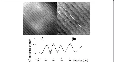
Figure 1a gives the scheme of one unit of coupled QDs lasing layers in one period. Figure 1b shows the atomic force microscopy (AFM) image of one-period QDCL with another unit of coupled QDs lasing layers (indi-cated by the dashed rectangle in Figure 1a) on top. The average diameter of QDs is about 30 nm, with a height of 2.5 nm. The entire structural quality of the QDCL wafer was confirmed by the X-ray diffraction (XRD) spectrum as shown in Figure 1c. In the XRD simulation, we treated the QD layer as a two-dimensional InAs layer with a homogeneous thickness corresponding to the
nominal deposit amount, which was strained biaxially to match the lattice constant of InP. The experimental zer-oth peak shows a nearly perfect lattice match to the InP substrate, which demonstrates that the active region layers have been properly strain-balanced to give a net zero strain. The accurate match of the simulated curve and the experimental curve shows an extremely good control over the growth parameters across the entire 30-period layer sequences. The cross-sectional view of transmission electron microscopy (TEM) images of a portion of the 30-period QDCL shown in Figure 2a,b gives the direct and clear evidences of distinct coupled QDs layers in the active core. What is more, the X-ray energy dispersion spectra (EDS) result obtained along cross section line of coupled QDs layers gives indium contents at different points. The ‘star’ represents the discrete data point of X-ray energy dispersion spectrum at each position along cross section line (Figure 2b) of coupled QDs layers of the TEM sample. Based on the fi-nite scattered experimental data points, we sketch the continuous curve of indium composition along cross section line with periodic oscillation characteristic. The periodic oscillation characteristic of indium relative
contents as shown in Figure 2c gives the additional evi-dence of QDs in the active region. This result is con-sistent with the AFM one.
A schematic conduction band diagram of one period of the active layers is shown in Figure 3a. The design computation is based on 1D Schroedinger equation of envelope function approximation from the point of view of simplicity. The energy dependence of the effective mass and the strain effect are included in the calcula-tion. The transition energy of 196 meV between states 9 and 8 is consistent with the experiment lasing wave-length. We also calculate the 3D coupled quantum dot states in the active region, which have about the same eigenenergy with the lower states in the simple 1D model, which implies that QD states as the final levels really contribute a lot to the electron-stimulated transi-tion in the active region and the effectiveness of the sim-ple 1D model.
[image:4.595.57.539.384.662.2]We present here a novel design to form upper hybrid QW/QD lasing states and lower pure QD lasing states to realize the‘phonon bottleneck’effect. A general scheme of the electron energy versus in-plane wave vector rela-tions is shown in Figure 3b. Although the states still have
Figure 3Energy band diagram. (a)Calculated conduction band diagrams of one period of the 30-stage QDCL active core under an electric field of 57 kV/cm using 1D model. The wavy curves represent the moduli squared of the wave functions of the relevant quantum states. The optical transition takes place between states 9 and 8.(b)Schematic illustration of electron energy (E) versus in-plane wave vector (Kin-plane) relation for
free particle-like dispersion skeleton in the direction paral-lel to the layers, the lateral quantum confinement breaks the subbands into quasi-continuous or discrete states. The upper hybrid subband (consists of hybrid-quantized states of QWs and QDs) is quasi-continuous, but the lower QD subband consists of widely separated in-plane energy states due to the lateral confinement of QDs. An electron in the upper quasi-continuous subband which relaxes to lower quantized states is difficult to obtain due to lack of appropriate final states. As a consequence, the relaxation time for the single-phonon process is increased. This im-plies that the nonradiative LO-phonon-assisted electron relaxation time in a QD is enhanced by a factor that de-pends on the lateral size of the QD. Figure 3c depicts the relevant energy levels and the electron injection/extraction sketch.
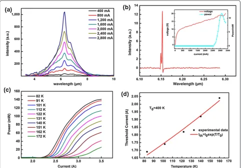
Figure 4a shows the spontaneous emission spectra of one such laser at room temperature for different drive
currents using Bruker Equinox 55 FTIR spectrometer. The spontaneous emissions at low drive currents display a full width at half maximum of 550 cm−1(broad emis-sion spectrum spanning the wavelength range of 4.5 to 7.5 μm). The very broad emission spectra confirm the typical characteristic of a broad gain medium provided by self-assembled QDs' inherent spectral inhomogeneity. We attribute the narrow peak on top of the broad base to a group of QDs in the active region with special size and then special QD energy states. These QDs are quite many in quantity, and the positions of their energy states in the energy band diagram are propitious for subse-quent electron extraction after transition. Figure 4b presents typical lasing spectrum obtained at 81 K near the laser threshold utilizing Nicolet 8700 FTIR spectrometer with a resolution of 0.125 cm−1. Mainly stemming from the bad waveform generated by the pulsed current source (PCX-7410), we cannot get the
Figure 4Spectra, power, and temperature characteristics. (a)Emission spectra from QDCL recorded at room temperature for different drive currents with a pulsed width of 1μs and repetition frequency of 50 kHz.(b)Typical lasing spectrum from the QDCL recorded at 81 K with a pulsed width of 2μs and repetition frequency of 1.5 kHz. The inset shows the voltage-current power curves.(c)Light-current (L-I) characteristics of QDCL operated in pulsed mode with a pulsed width of 2μs and repetition frequency of 5 kHz.(d)Threshold current as a function of heat sink temperature in pulsed operation for another typical laser device. The solid curve represents fit using the empirical exponential function,
classical multi-longitudinal-mode lasing spectra. The distinct lasing takes place at wavelength of 6.15μm, which is consistent with the calculated transition energy of 196 meV between states 9 and 8 indicated in Figure 3a. The laser still works up to 250 K according to the spectra results of our FTIR spectrometer. However, due to the unoptimized device processing, especially the possible current leakage of SiO2 insulating layer under relatively
high voltage (the accessorial experiment proved that the SiO2layer was somewhat loose, which can lead to pinhole
leakage), the prototype device cannot perform lasing over room temperature. Moreover, the voltage-current power curves as the inset of Figure 4b show the energy band alignment voltage of about 10 V.
Figure 4c shows the light power (L) versus current (I) characteristics of laser for different heat sink tempera-tures. A peak optical power of more than 140 mW at 82 K was measured, with a threshold current density of about 4 kAcm−2. The large threshold current density may stem from a number of factors, including the broad gain spectrum, the energy misalignment between in-jector and bound state 9, electron leakage to higher spurious states, over-discrete and inhomogeneous lower energy states due to size inhomogeneity of QDs, pos-sible parasitical bound state between states 9 and 8, ex-traction efficiency of electron from low miniband not optimized, and thermal backfilling. Figure 4d shows the temperature dependence of the threshold current for another typical laser. AT0value of 400 K is obtained
within the temperature range of 82 to 162 K. This relative highT0is also the inherent characteristic of QDs-based
lasers [29-31].
Figure 5 gives the PC spectra of samples under different temperatures and zero bias and demonstrates the strong perpendicular response of our materials. The spectra peak at about 1,900 cm−1, showing reasonable agreement with the computed result. The inset of Figure 5 is a calculated 1D conduction band diagram of one period of the 30-stage QDCL active core under zero bias from the point of view of simplicity. The energy difference between the upper lasing level (bold) and the lowest energy level corre-sponds to 1,790 cm−1. Meanwhile, we conducted some other photocurrent experiments using several normal strain-compensated quantum cascade laser (QCL) wafers with the same processing and found that their photo-current is two or three orders of magnitude smaller than our QDCLs, which demonstrates the effect of QDs in our QDCL active region. Theoretically, normal QCL wafer does not absorb perpendicularly incident infrared light due to transition selection rule. Meanwhile, in our wafer with QDs in the active region, electrons experi-ence the confinement from the direction in the growth plane. So according to the transition selection rule, QDCL wafer should respond to the perpendicularly incident light
strongly and the experimental results confirm the QDs' effect in our sample.
Conclusions
In conclusion, we believe that the reported structure does show quantum dot characteristics from the AFM, TEM, EDS, EL,T0, and PC measurements and to some extent,
limited phonon bottleneck effects. Moreover, by improved design of the QDs-based active region of our device, in particular, aiming at the controllability on QDs size and smart two-step strain compensation, we also be-lieve that the overall performance of QDCLs will be a great leap forward. What is more, our QDCL design concept can be transplanted to terahertz quantum cascade laser design, paving a new way for room temperature operation.
Abbreviations
AFM:atomic force microscopy; EDS: energy dispersion spectra; FTIR: Fourier transform infrared; MBE: molecular beam epitaxy; ML: monolayer; MOCVD: metal-organic chemical vapor deposition; QDs: quantum dots; QDCL: quantum dot cascade laser; QWs: quantum wells; TEM: transmission electron microscopy; XRD: X-ray diffraction.
Competing interests
The authors declare that they have no competing interests.
Authors' contributions
[image:6.595.306.539.88.260.2]NZ designed the laser core structure, fabricated the device, performed the testing, and wrote the paper. FQL provided the concept, grew the wafer, wrote the paper, and supervised the project. JZ, LW, and JL fabricated the device and performed the testing. SZ grew the wafer. ZW supervised the project. All authors read and approve the final manuscript.
Figure 5Photocurrent spectra of samples under different temperatures and zero bias.The PC measurements were conducted using Bruker Equinox 55 FTIR spectrometer under step-scan mode with a resolution of 16 cm−1. The IR beam was chopped before
Acknowledgements
This work was supported by the National Research Projects of China (Grant Nos. 2013CB632800, 60525406, 60736031, and 2011YQ13001802-04).
Received: 12 February 2014 Accepted: 12 March 2014 Published: 25 March 2014
References
1. Faist J, Capasso F, Sivco DL, Sirtori C, Hutchinson AL, Cho AY:Quantum cascade laser.Science1994,264:553–556.
2. Yao Y, Hoffman AJ, Gmachl CF:Mid-infrared quantum cascade lasers.
Nat Photon2012,6:432–439.
3. Lyakh A, Maulini R, Tsekoun A, Go R, Pflügl C, Diehl L, Wang QJ, Capasso F, Patel CKN:3 W continuous-wave room temperature single-facet emission from quantum cascade lasers based on nonresonant extraction design approach.Appl Phys Lett2009,95:1411103.
4. Bai Y, Bandyopadhyay N, Tsao S, Slivken S, Razeghia M:Room temperature quantum cascade lasers with 27% wall plug efficiency.Appl Phys Lett 2011,98:181102.
5. Lu QY, Bai Y, Bandyopadhyay N, Slivken S, Razeghia M:2.4 W room temperature continuous wave operation of distributed feedback quantum cascade lasers.Appl Phys Lett2011,98:181106. 6. Williams BS:Terahertz quantum-cascade lasers.Nat Photon2007,
1:517–525.
7. Kohler R, Tredicucci A, Beltram F, Beere HE, Linfield EH, Davies AG, Ritchie DA, Iotti RC, Rossi F:Terahertz semiconductor-heterostructure laser.Nature2002, 417:156–159.
8. Belkin MA, Capasso F, Belyanin A, Sivco DL, Cho AY, Oakley DC, Vineis CJ, Turner GW:Terahertz quantum-cascade-laser source based on intracavity difference-frequency generation.Nat Photon2007,1:288–292.
9. Lu QY, Bandyopadhyay N, Slivken S, Bai Y, Razeghi M:Room temperature single-mode terahertz sources based on intracavity difference-frequency generation in quantum cascade lasers.Appl Phys Lett2011,99:131106. 10. Fathololoumi S, Dupont E, Chan CWI, Wasilewski ZR, Laframboise SR, Ban D,
Matyas A, Jirauschek C, Hu Q, Liu HC:Terahertz quantum cascade lasers operating up to∼200 K with optimized oscillator strength and improved injection tunneling.Opt Express2012,20:3867–3876.
11. Hugi A, Terazzi R, Bonetti Y, Wittmann A, Fischer M, Beck M, Faist J, Gini E: External cavity quantum cascade laser tunable from 7.6 to 11.4μm.Appl
Phys Lett2009,95:061103.
12. Faist J:Wallplug efficiency of quantum cascade lasers: critical parameters and fundamental limits.Appl Phys Lett2007,90:253512.
13. Lyakh A, Pflügl C, Diehl L, Wang QJ, Capasso F, Wang XJ, Fan JY, Tanbun-Ek T, Maulini R, Tsekoun A, Go R, Patel CKN:1.6 W high wall plug efficiency, continuous-wave room temperature quantum cascade laser emitting at 4.6μm.Appl Phys Lett2008,92:111110.
14. Bai Y, Slivken S, Darvish SR, Razeghia M:Room temperature continuous wave operation of quantum cascade lasers with 12.5% wall plug efficiency.Appl Phys Lett2008,93:021103.
15. Liu PQ, Hoffman AJ, Escarra1 MD, Franz1 KJ, Khurgin JB, Dikmelik Y, Wang X, Fan J, Gmachl CF:Highly power-efficient quantum cascade lasers.
Nat Photon2010,4:95–98.
16. Bai Y, Slivken S, Kuboya S, Darvish SR, Razeghi M:Quantum cascade lasers that emit more light than heat.Nat Photon2010,4:99–102.
17. Liverini V, Bismuto A, Nevou L, Beck M, Faist J:Midinfrared
electroluminescence from InAs/InP quantum dashes.Appl Phys Lett2010, 97:221109.
18. Wingreen NS, Stafford CA:Quantum-dot cascade laser: proposal for an ultralow-threshold semiconductor laser.IEEE J Quantum Electron1997, 33:1170–1173.
19. Zhang ZY, Wang ZG, Xu B, Jin P, Sun ZZ, Liu FQ:High-performance quantum-dot superluminescent diodes.IEEE Photon Technol Lett2004, 16:27–29.
20. Wassermana D, Lyon SA:Midinfrared luminescence from InAs quantum dots in unipolar devices.Appl Phys Lett2002,81:2848–2850.
21. Anders S, Rebohle L, Schrey FF, Schrenk W, Unterrainer K, Strasser G: Electroluminescence of a quantum dot cascade structure.Appl Phys Lett 2003,82:3862–3864.
22. Brault J, Gendry M, Grenet G, Hollinger G, Desieres Y, Benyattou T:Role of buffer surface morphology and alloying effects on the properties of InAs nanostructures grown on InP(001).Appl Phys Lett1998,73:2932–2934.
23. Schwertberger R, Gold D, Reithmaier JP, Forchel A:Long-wavelength InP-based quantum-dash lasers.IEEE Photon Technol Lett2002,14:735–737.
24. Schwertberger R, Gold D, Reithmaier JP, Forchel A:Epitaxial growth of 1.55μm emitting InAs quantum dashes on InP-based heterostructures by GS-MBE for long-wavelength laser applications.J Cryst Growth2003, 251:248–252.
25. Sauerwald A, Kümmell T, Bacher G, Somers A, Schwertberger R, Reithmaier JP, Forchel A:Size control of InAs quantum dashes.Appl Phys Lett2005, 86:253112.
26. Reithmaier JP, Somers A, Deubert S, Schwertberger R, Kaiser W, Forchel A, Calligaro M, Resneau P, Parillaud O, Bansropun S, Krakowski M, Alizon R, Hadass D, Bilenca A, Dery H, Mikhelashvili V, Eisenstein G, Gioannini M, Montrosset I, Berg TW, Poel MVD, Mørk J, Tromborg B:InP based lasers and optical amplifiers with wire-/dot-like active regions.J Phys D2005, 38:2088–2102.
27. Djie HS, Tan CL, Ooi BS, Hwang JCM, Fang XM, Wu Y, Fastenau JM, Liu WK, Dang GT, Chang WH:Ultrabroad stimulated emission from quantum-dash laser.Appl Phys Lett2007,91:111116.
28. Zhang JC, Liu FQ, Tan S, Yao DY, Wang LJ, Li L, Liu JQ, Wang ZG: High-performance uncooled distributed-feedback quantum cascade laser without lateral regrowth.Appl Phys Lett2012,100:112105. 29. Botez D, Kumar S, Shin JC, Mawst LJ, Vurgaftman I, Meyer JR:Temperature
dependence of the key electro-optical characteristics for midinfrared emitting quantum cascade lasers.Appl Phys Lett2010,97:071101. 30. Fujita K, Yamanishi M, Edamura T, Sugiyama A, Furuta S:Extremely high
T0-values (450 K) of long-wavelength (15μm), low-threshold-current-density quantum-cascade lasers based on the indirect pump scheme.Appl Phys
Lett2010,97:201109.
31. Bai Y, Bandyopadhyay N, Tsao S, Selcuk E, Slivken S, Razeghia M:Highly temperature insensitive quantum cascade lasers.Appl Phys Lett2010, 97:251104.
doi:10.1186/1556-276X-9-144
Cite this article as:Zhuoet al.:Quantum dot cascade laser.Nanoscale
Research Letters20149:144.
Submit your manuscript to a
journal and benefi t from:
7Convenient online submission
7Rigorous peer review
7Immediate publication on acceptance
7Open access: articles freely available online
7High visibility within the fi eld
7Retaining the copyright to your article