IMPLEMENTATION OF MODIFIED REDUCED SWITCH MULTILEVEL
INVERTER USING MCPWM AND MSPWM TECHNIQUES
V. Sudha and K. Vijayarekha
Shanmugha Arts, Science, Technology and Research Academy, Thanjavur, India E-Mail: [email protected]
ABSTRACT
The Multilevel inverters are used to obtain the desired AC voltage from several levels of DC voltage and also reduce the filter requirement in the system. It has more advantages when compared to traditional two level inverter. This paper proposes Multi carrier pulse width modulation (MCPWM) and multiple sinusoidal pulse width modulation techniques (MSPWM) based Modified Multilevel Inverter with reduced number of switches. Reduced harmonic distortion is achieved in the output voltage waveform without reduction in the output power using these techniques. The inverter is able to produce seven and nine levels from the dc supply source. The analysis has been made based on the Total Harmonic Distortion (THD). The pulse width modulation techniques used in this paper are MSPWM and MCPWM with triangular wave as carrier wave. The proposed inverter is simulated in Matlab/Simulink. The hardware prototype implementation is done using Power MOSFET switches and the THD is analysed using Power Quality Analyser.
Keywords: multilevel inverter, multicarrier pulse width modulation, multiple sinusoidal pulse width modulation, total harmonic
distortion.
1. INTRODUCTION
Power electronic converters are becoming familiar and are implemented for medium as well as high power applications. The electronic device which converts fixed DC voltage to a variable AC voltage is known as inverter. The output may be a variable voltage and variable frequency. Multilevel converters were used with a normal three level inverter. Multilevel inverters are the power electronics voltage synthesizers in which the output voltage level can be increased in steps to a stair case waveform [1-3]. The output voltage levels are increased to achieve an approximate sinusoid. Hence the reduction of Total Harmonic Distortion (THD) is achieved [3]. When compared to two level inverter, multilevel inverter has advantages like minimum distortions, least components, lower switching loss and high efficiency [4-9]. D iode-clamped MLI, Flying capacitor MLI and Cascaded MLI are different topologies of multilevel inverters. Cascaded inverter has simple structure when compared to Diode clamped inverter and Flying capacitor inverter [10]. Diode clamped inverter is restricted to five levels only, because of the unbalanced voltage across capacitors. The General cascaded MLI is shown in figure1 and from the figure it was inferred that the General Cascaded MLI needed 12 semiconductor switches for a seven level output. The Modified Cascaded Multilevel inverter consists of only 8 IGBT switches and 8 diodes for seven level and for nine level 10 IGBT switches and 10 diodes are used [11-16].Thus by using this Modified Cascaded Multilevel inverter the switching losses are reduced because the power semiconductor switches are reduced and the complexity of circuit minimized.
2. CASCADED MULTILEVEL INVERTER
The normal cascaded H-bridge Inverter consists of a series connection of H-bridges and contains four switches in each cell. The universal function of this multilevel inverter (MLI) is to combine a required voltage
from several input dc sources. The input DC sources are connected to each converter cell. The resultant output voltage is addition of voltages generated via different H-Bridges. The resultant output ac voltage varies from -4Vdc to +4Vdc [14-16]. The general cascaded 9 levels MLI consists of 10 semiconductor switches and 4 separate DC sources.
Figure-1. General cascaded MLI circuit.
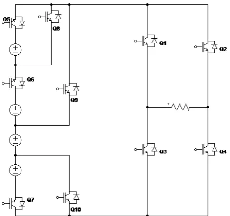
3. MODIFIED CASCADED MULTILEVEL INVERTER
manner as shown in the Figure-2 for nine levels. The number of switches involved is increased by two for every level increment and similarly this topology can be expanded up to n number of levels. Table-1 shows the comparison of switches required for the conventional cascaded MLI and the modified cascaded MLI for the nine levels.
[image:2.595.52.288.185.406.2]Figure-2. Modified cascaded MLI with reduced switches.
Table-1. Comparison of switches.
Levels
Switches required
Cascaded MLI Modified Cascaded Multilevel Inverter
5 8 6
7 12 8
9 16 10
11 20 12
13 24 14
4. OPERATION OF MODIFIED CASCADED MLI The modified nine level inverter consists of ten switches along with four dc voltage sources. The circuit diagram for nine level inverter of proposed topology is shown in figure 2. The nine level output voltages are +Vdc, +2Vdc, +3Vdc, +4Vdc, 0, -Vdc,-2Vdc,-3Vdc,, -4Vdc. The operation of conducting switches for nine level is shown in table 2. For getting +Vdc diodes D9, D10 are ON and the load is connected to Q1 with respect to Q4. For getting +2Vdc auxiliary switch Q7 is ON and the load is connected to Q1 with respect to Q4.Now the upper two sources are connected in series via Q7, Q1, load, Q4, and D10.For +3Vdc auxiliary switches Q7, Q6 is ON, load terminal positive is connected to main switch Q1 and negative terminal to Q4.For –Vdc,-2Vdc,-3Vdc,- 4Vdc the main switches Q2 and Q3 is in ON state instead of Q1 and Q4 and the remaining
switches operation are similar. For zero level auxiliary switch Q9 or Q10 is alone in ON state. This topology can be extended up to n number of levels and the generalized multilevel inverter configuration of the new topology as given in Figure-3.
Table-2. Switching table for modified cascaded multilevel inverter.
Duration Switches to be turn on
Diodes that conducts
Voltage levels
Positive Half Cycle
Q9,Q10 - 0
Q1,Q4 D9,D10 Vdc
Q1,Q4,Q7 D9 2Vdc
Q1,Q4,Q6,Q7 D8 3Vdc
Q1,Q4,Q5,Q6,Q7 - 4Vdc
Negative Half Cycle
Q9,Q10 - 0
Q2,Q3 D9,D10 -Vdc
Q7, Q2,Q3 D9 -2Vdc
Q6,Q7, Q2,Q3 D8 -3Vdc
Q5,Q6,Q7, Q2,Q3 - -4Vdc
Figure-3. Generalized multilevel inverter configuration of the new topology.
5. MODULATION STRATEGIES
A. MCPWM strategy
[image:2.595.310.548.190.658.2] [image:2.595.51.289.450.585.2]method, APOD method, POD method, Variable frequency method.
a) PD (phase disposition) PWM
In this technique all the carriers are in phase with each other as given in Figure-4. All carrier signals are having the same amplitude and frequency.
Figure-4. PD method.
b) APOD (Alternative phase opposition disposition) PWM
In this technique every carrier signals are alternately phase shifted by 180 degrees as given in Figure-5.
In this method also all carrier signals are having the same amplitude and frequency [20].
Figure-5. APOD method.
c) Variable frequency PWM (VFPWM)
In this method all the carriers are in phase with same amplitude with different frequency as given in Figure-6.
Figure-6. Variable Frequency method.
B. MSPWM strategy
In this technique, multiple sinusoidal signals are compared to a single carrier to get the gate signals of required pulse width [9]. For the seven level output, three sinusoidal waveforms with equal amplitude and equal frequency are compared with a single carrier and gate pulses are generated similarly for nine level four sinusoidal modulation signals compared with single carrier wave. Am is the amplitude and fm is the frequency of the modulation signals. The following equation defines modulation index ma as
ma = Am/ (N-1)/2*Ac Where, N is the number of levels.
The frequency modulation ratio mf is given by mf = fc / fm.
Figure-7. MSPWM strategy.
6. SIMULATION RESULTS
The simulation for the proposed configuration is done with help of MATLAB/SIMULINK. The simulation diagram for the proposed MLI for seven levels is given in Figure-8. The load used in the simulation is RL load. Each input DC supply has the value of 200V. Switching frequency is 5 kHz.
Figure-8. MATLAB/Simulink model of modified cascaded 7-level inverter.
A) PDPWM technique
a) Seven level PDPWM technique
Figure-9. (a) Output voltage (b) Harmonic analysis.
b) Nine level PDPWM technique
The output voltage waveform and FFT analysis for corresponding THD value for nine level using PDPWM techniques is given in the Figure-10.
Figure-10. (a) Output voltage (b) Harmonic analysis.
B) APODPWM technique
a) Seven level APODPWM technique
He output voltage waveform and FFT analysis for corresponding THD value for seven level using APODPWM technique is given in the Figure-11.
Figure-11. (a) Output Voltage (b) Harmonic analysis.
b) Nine level APODPWM technique
The output voltage waveform and FFT analysis for corresponding THD value for nine level using APODPWM techniques is given in the Figure-12.
Figure-12. (a) Output voltage (b) Harmonic analysis.
C) VFPWM technique
a) Seven level VFPWM technique
The output voltage waveform and FFT analysis for corresponding THD value for seven level using VFPWM techniques is given in the Figure-13.
Figure-13. (a) Output voltage (b) Harmonic analysis.
b) Nine level VFPWM technique
The output voltage waveform and FFT analysis for corresponding THD value for nine level using VFPWM techniques is given in the Figure-14.
Figure-14. (a) Output voltage (b) Harmonic analysis.
D) MSPWM technique
a) Seven level MSPWM technique
The output voltage waveform and FFT analysis for corresponding THD value for seven level using MSPWM techniques is given in the Figure-15.
Figure-15. (a) Output voltage (b) Harmonic analysis.
b) Nine level MSPWM technique
Figure-16. (a) Output voltage (b) Harmonic analysis.
Table-3. THD comparison chart.
Methods Seven level (THD %)
Nine level (THD %) PD method 12.71 % 11.17 %
APOD method 17.22 % 15.50 %
VFPWM method 21.07 % 15.19 %
MSPWM method 22.82% 18.89 %
7. HARDWARE IMPLEMENTATION
The hardware has been implemented for seven level inverter using PDPWM technique. The gating signals are generated using PIC16F877A microcontroller. Gate Driver circuits are used for boosting the pulses from a microcontroller. The IRF540 - MOSFETs are used in this design which has high voltage and current carrying capability. The THD value has been analyzed using power quality analyzer and the value is 13.33% compared to 12.71% calculated from simulation. The prototype for seven level multilevel inverter is shown in figure 17 and the output voltage for seven level multilevel inverter
measured by the power quality analyzer is shown in Figure-17.
Figure-17. Hardware setup for PDPWM based seven level inverter.
Figure-18. Hardware output voltage waveform.
Table-4. Comparison chart.
PDPWM method THD (%)
SIMULINK Software
MATLAB Version 7.9 12.71 Hardware Implementation 13.33
8. CONCLUSIONS
In this paper four PWM techniques of modified cascaded seven and nine level inverter has been simulated.
Out of four PWM techniques, PDPWM control technique of modified cascaded inverter is best based on the FFT analysis observed from the simulation results. The simulation result also shows that the THD get reduced for increase in higher voltage levels. The size of the inverter is reduced since the required number of components is less compared to conventional H bridge inverter. Thus the modified multi level inverter with PDPWM method control technique is validated through the detailed simulation analysis and experimentation.
The hardware and simulation results were compared based on the aspects of total harmonic distortion. This inverter can be a solution to solar based grid connected system.
REFERENCES
[1] Usman Bashir Tayab and Muhammad Adnan Bashir. 2017. Multilevel inverter topologies for Photovoltaic Power System: A Review. ARPN Journal of Engineering and Applied Sciences. 12(11): 3537-3549.
[2] Sayat Moldakhmetov, Nalik Issembergenov, Dauren Insepov and Seitzhan Orynbayev. 2016. Implementation of Multilevel Power Inverter. ARPN Journal of Engineering and Applied Sciences. 11(11): 6886-6890.
[3] J. Rodríguez, J.S. Lai, and F.Z. Peng. 2002. Multilevel Inverters: A Survey of Topologies. IEEE Transactions on Industrial Applications. 49(4): 724-738.
[4] Sayat Moldakhmetov, Nalik Issembergenov and Abdurazak Kasymov. 2015. Multilevel inverter based on level switch and H-bridge. ARPN Journal of Engineering and Applied Sciences. 10(16): 6884-6887.
[5] K. Selvamuthukumar, M. Satheeswaran and A. Ramesh Babu. 2015. Single Phase Thirteen Level Inverter with reduced number of switches using different modulation techniques. ARPN Journal of Engineering and Applied Sciences. 10(22): 10455-10462.
[6] Vinod Kumar, Ch. Santosh Kumar and K. Ramesh Reddy. 2013. Single Phase Cascaded Multilevel Inverter using Multicarrier PWM Technique. ARPN Journal of Engineering and Applied Sciences. 8(10): 796-799.
[7] Rashmy Deepak, Vishnu S. Kasturi, Lepakshi Sarkar, Y.R. Manjunatha, B.R. Lakshmikanthal. 2014. Novel multilevel inverter with reduced number of switches and batteries. IEEE Xplore.
[8] Shanthi and S.P. Natarajan. 2011. Comparative Study on Carrier Overlapping PWM strategies for Five Level Diode Clamped Inverter. International Journal on Electrical Engineering and Informatics. 3(1)
[9] Rosli Omar, Mohammed Rasheed, Marizan Sulaiman. 2015. Comparative Study of a Three Phase Cascaded H-Bridge Multilevel Inverter for Harmonic Reduction. International Journal on Electrical Engineering and Informatics. 14(3): 481-492.
[10] K.Surya Suresh and M. Vishnu Prasad. 2012. Analysis and Simulation of New Seven Level Inverter Topology. International Journal of Scientific and Research Publications. 2: 1-6.
[11]Manu Jacob T Sreeja E.A. 2016. Multilevel Inverter with Reduced Number of Switches using Multi Carrier Phase Opposition Disposition PWM. International Journal for Innovative Research in Science & Technology. 3: 121-125.
[12]A. Gnana Prakash, M. Balamurugan, S. Umashankar. 2014. New Multilevel Inverter with Reduced Number of Switches. International Journal of Power Electronics and Drive System. 5: 63-70.
[13]Nimitha Muraleedharan, T.Remani. 2014. Simulation and analysis of multilevel inverter with reduced number of switches. International Journal of Electrical Engineering & Technology. 5:21-31.
[14]C. Udhaya Shankar, J. Thamizharasi, Rani Thottungal, N. Nithyadevi. 2012. Harmonic reduction in Cascaded Multilevel Inverter with reduced number of switches using Genetic Algorithms. International journal of advances in engineering & technology. 3.284-294.
Journal of Advanced Research in Electrical, Electronics and Instrumentation Engineering. 6: 539-545.
[16]Sathish Cherukuru, Clinton Joel. C, Sahaya Jeenson Jonish. A, Dr. K. Sathiyasekar. 2014. New Modified Cascaded H-Bridge Multilevel Inverter Topology with Reduced Switches. International Journal of Engineering Trends and Technology. 9(4): 178-181.
[17]A. Radan, A.H. Shahirinia, M. Falahi. 2007. Evaluation of Carrier-Based PWM Methods for Multi-level inverters. IEEE. 389-394.
[18]Mariusz Malinowski, K. Gopakumar, Jose Rodriguez, and Marcelo A. Perez. 2010. A Survey on Cascaded Multilevel Inverters. IEEE Transactions on Industrial Electronics. 57(7): 2197-2205.
[19]B.P. McGrath and Holmes. 2002. Multicarrier PWM strategies for multilevel inverter. IEEE Transactions on Industrial Electronics. 49(4): 858-867.