International Journal of Emerging Technology and Advanced Engineering
Website: www.ijetae.com (ISSN 2250-2459, ISO 9001:2008 Certified Journal, Volume 2, Issue 12, December 2012)
542
Verification and Simulation of New Designed NAND Flash
Memory Controller
Koushel Agarwal
1, Vijay Kumar Magraiya
2, Dr. Anil Kishore Saxena
31
Research scholar,
Electronics and Comm. dept.,
SRCEM Banmore,
Morena, India
2Assistant Professor, Electronics and Comm. dept.,SRCEM Banmore,Morena, India 3Director, SRCEM Banmore,Morena, India
Abstract— In this paper a NAND flash memory controller was designed. For the better use of NAND type flash memory we design a new Arithmetical and Logical Unit (ALU) for calculating addition, subtraction, increment, decrement operations etc. In this memory controller we design a decoder, single memory cell, memory module etc. These all are encapsulated inside a controller and this is on top most in hierarchy. As the cell size of NAND flash memory is reduced every year the performance, reliability, speed is increased very rapidly. NAND flash memory is programmed on page by page basis. Typically programming time is very less few micro second per page. This NAND flash memory controller architecture can be used with a real secure digital card, multimedia card (SD/MMC), digital cameras etc. Experimental results show that the designed controller give good performance and full fill all the system specifications. We design and implement FPGA based open framework for fast, correct features of flash memories.
Keywords-Flash memory; Arithmetical and Logical Unit (ALU); Encapsulation; Field Programmable Gate Array (FPGA);
I. INTRODUCTION
NAND flash memory device is a non volatile storage media even if power is switch off. NAND flash memory is widely used in semiconductor industry for its high performance, low cost, high capacity, high speed, and low power consumption solid state data storage drive. It is mainly used in variety of applications like MP3 players, digital cameras, mobile phones, removable memory card, pan drive etc. Due to high performance several cross interfaces between memory cells is required.
Traditional Hard Disk Drive (HDD) is now replaced by flash memory in various embedded computing systems because flash memory is always good in all the above parameters and it gives a very high performance on a very low cost. To improve the input output bandwidth we have a multi Chanel parallel access mechanism in the flash array [5]. Flash memory controller offers higher capacity for fast data transfer and random access of memory in I/O operations [1]. It is possible to design a simple memory mapped interface to hardware with NAND flash memory. NAND flash memory controller is always enhance the reliability of flash memory.
NAND flash memory controller has also a bidirectional bus in between peripheral devices and controller, controller internal bus for various functional blocks and controller with memory connections. These buses travel all the I/O data as well as control and address signals from one place to another. For the improvement of product lifetime and system performance we always design an excellent NAND flash memory controller. Single Level Cell (SLC) and Multi Level Cell (MLC) two techniques are used for storing data in memory cells. SLC offers 100,000 erase program cycle while MLC offers about 10,000 erase program cycle [2].
In NAND flash memory cell are arranged in series with sharing of source and drain, simply NMOS transistors are arranged for building NAND gate [6]. So sharing the source and drain of adjacent cells eliminate need for metal contact and reduce the die size. NAND flash cells placed together for saving 60% cell size over NOR flash cells. In nor flash cells arrange in parallel with all source node of the cells connected as a NMOS transistors are arranged for building NOR gate. A software called Flash Transaction layer (FTL) use for wear leveling and bad block management technique. All vendors provide FTL software [9].
The systolic array architecture and iterative Very Large Scale Integration (VLSI) architecture in applied for good performance. The pipelining and parallel processing concepts are applied for systematic design approach of a systolic array processor. It makes the circuit design easy for implementation. NAND flash memory controller provides a serial access of data blocks in a very high speed [8].
.
II. NAND FLASH MEMROY CONTROLLER ARCHITECHTURE
International Journal of Emerging Technology and Advanced Engineering
Website: www.ijetae.com (ISSN 2250-2459, ISO 9001:2008 Certified Journal, Volume 2, Issue 12, December 2012)
[image:2.612.70.295.193.361.2]543 In multiplane array packs all operations performs parallels. Inside a single flash array operation time multiple pages of data can be programmed, read, write, fetched etc. so average data access time is small. In multiplane commands some addresses are restricted.
Figure 1. Block Diagram of a NAND Flash Memory Controller
NAND flash controller has flash chips. In today life it is widely used in storage devices. At many applications it is a very good replacement of hard disk drive because its low cost, high performance, low power consumption etc. NAND flash controller receives data and commands signals from computer and translates it into a set of commands to flash chips. It always follows Open NAND Flash Interface (ONFI) standard [3].
In NAND flash device we have mainly I/O control block, control logic, NAND flash array. A NAND flash array includes two dimensional NAND flash cells, Row/Column address decoder and cache / data registers [11]. It has a shared, multiplexed, bidirectional (command, address and data) I/O bus. Figure-1 shows the block diagram of a NAND Flash Memory Controller.
A multidie array packs have multiple dies on one chip. All are independent in operations and share a common data, address and command bus. So page programmed event, page erase event, command through the chip level I/O interface event are performed parallels with in a chip. So new NAND flash chip with multidie and multiplane support is always increase performance, reduce the data access average time, and increase parallel execution of commands [7].
NAND flash devices are programmed on a page by page basis. Typically programming time is a few hundred micro second per page. ONFI provides a common standard for different flash devices.
So future extension and interfacing is possible and it is very easy. NAND flash cell can be programmed and
erased only for limited time period (100,000 times for SLC and 10,000 times for MLC) before it fails. We always want to improve this limitation so flash memory performance is increased. They all provide an FPGA to facilitate the implementation of a wide range of NAND Flash Memory Controller [4].
III. SIMULATION AND RESULT A. Single Micro cell Module
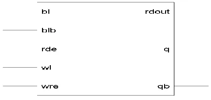
[image:2.612.325.565.387.668.2]In the simulation result the NAND flash memory cell is simulated using Xilinx ISE Software and modelsim simulator. As shows in Figure-2 the RTL view of NAND Flash memory cell was generated after the synthesis and it is display the internal architecture of NAND Flash memory cell. The modelsim waveform is display on Figure-3 and it is indicate the write and read operation. Write operation takes place only when both word line and write enable are „1‟. The q and qbar line are modified when this situation is made as seen in the wave form and Read operation takes place from the cell both word line and read enable should be high so that read out shows the data stored in q.
Figure 2. RTL Schematic View of Single Micro Cell
[image:2.612.346.562.391.493.2]International Journal of Emerging Technology and Advanced Engineering
Website: www.ijetae.com (ISSN 2250-2459, ISO 9001:2008 Certified Journal, Volume 2, Issue 12, December 2012)
544
B. Full Adder
In the simulation of full adder using Xilinx ISE Software and modelsim simulator. As shows in Figure-4 the RTL view of full adder was generated after the synthesis and it is display the internal architecture of full adder. The modelsim waveform is display on Figure-5 and it is indicate the sum and carry operation. Sum operation takes place only when any one input is high and carry operation are done when at least two inputs are high.
[image:3.612.333.560.168.278.2]Figure 4. RTL Schematic View of Full Adder
Figure 5. Simulation Waveform of Full Adder
C. Arithmetic and Logical Unit (ALU)
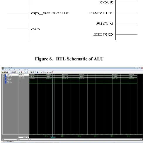
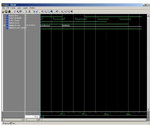
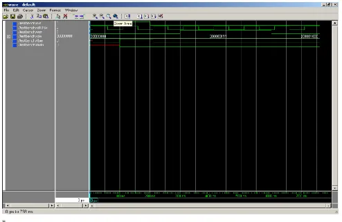
In the simulation result of Arithmetic and Logical Unit (ALU) using Xilinx ISE Software and modelsim simulator. As shows in Figure-6 the RTL view of ALU was generated after the synthesis and it is display the internal architecture of ALU. The modelsim waveform is display on Figure-7 and it is indicate all mathematical operation. In addition operation takes place only when op_sel ie. operation select lines are zero and provide input value to the dat_a and dat_b and check the results on dat_out as well as all flag register like carry flag, sign flag, auxiliary carry flag, parity flag, etc.
In the way we can calculate all mathematical operation with the help of only to change the value of op_sel. Full adder is call inside ALU.
[image:3.612.323.567.210.455.2]Figure 6. RTL Schematic of ALU
Figure 7. Simulation Waveform of ALU
D. Memory Module
[image:3.612.77.278.239.351.2]In the simulation result of Memory Module using Xilinx ISE Software and modelsim simulator. As shows in Figure-8 the RTL view of Memory Module was generated after the synthesis and it is display the internal architecture. The modelsim waveform is display on Figure-9 and it is indicate how the data can store in to the memory with the help of read and write operation.
[image:3.612.53.289.400.529.2] [image:3.612.340.554.583.685.2]International Journal of Emerging Technology and Advanced Engineering
Website: www.ijetae.com (ISSN 2250-2459, ISO 9001:2008 Certified Journal, Volume 2, Issue 12, December 2012)
[image:4.612.55.301.105.286.2]545 Figure 9. Simulation Waveform of Memory Module
E. Memory Read Cycle
As shows in Figure-10 the RTL view of memory read cycle was generated after the synthesis and it is display the internal architecture of Memory Read Cycle. The modelsim waveform is display on Figure-11. During Memory Read Cycle when reset = „1‟ then both the mode operation is zero and when apply the clock pulse the data at ¼ and ¾ points in data cell is generated and when increment the clock the data are in a position to goes from serial to parallel conversion after some time it will also shift to data register in this way data are shifted to the particular data register and finally read the data at that location.
Figure 10. RTL View of Memory Read Cycle
Figure 11. Simulation Waveform of Memory Read Cycle
F. Memory Write Cycle
As shows in Figure-12 the RTL view of Memory Write Cycle was generated after the synthesis and it is display the internal architecture of Memory Write Cycle. The modelsim waveform is display on Figure-13. During Memory Write Cycle when reset = „1‟ then both the wrn1 and wen2 operation is one and when enable the clock detect the edge on write pulse after some time detect edge on write pulse to load transmit buffer. When increment the clock the data are in a position to goes from transmit shift register to transmit buffer. In this way data are shifted to the particular data register and finally write the data at that location.
[image:4.612.323.568.114.320.2] [image:4.612.79.286.481.616.2] [image:4.612.334.558.512.643.2]International Journal of Emerging Technology and Advanced Engineering
Website: www.ijetae.com (ISSN 2250-2459, ISO 9001:2008 Certified Journal, Volume 2, Issue 12, December 2012)
546 Figure 13. Simulation Waveform of Memory Write
Cycle
G. NAND Flash Memory Controller
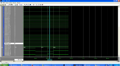
The Figure-14 shows Xilinx RTL Schematic view of NAND Flash Memory Controller. The Figure-15 are shows the Simulation Waveform of NAND Flash Memory Controller. We bind all the above components inside this module. This module is stand at the top of hierarchy. Various pins are described below-:
nand_ale : This indicate NAND Flash advanced latch enable when this pin is high the NAND Flash Memory Controller work and when it is low the NAND Flash Memory Controller are in latch mode.
nand_ce : This pin indicate NAND Flash chip enable. When this pin is high the NAND Flash Memory Controller are in working mode that is the data can store in a memory in sequential order. When it is low the NAND Flash Memory Controller not worked.
nand_cle : This pin indicate NAND flash clear mode. When this pin is high the data are cleared in the main memory of NAND Flash Memory Controller. When it is low it will worked.
nand_re : This pin indicates NAND Flash reset. When this pin is high the NAND Flash Memory Controller are in reset mode that is all operation of NAND Flash Memory Controller Stopped. When it is low it will worked properly.
nand_tri_en : This pin indicate NAND Flash tri-state enable. When it is high it will indicate the data are in tri-state that is high impedance state. When it is low it may be worked properly.
nand_we : This pin indicates NAND flash in write operation. When it is high data are write in a write mode that means we can write the data at particular memory address. When it is low it will not provide a permission to write the data.
nand_opr<2:0> : These pin indicates selection between read state (000), read ID state (001), read page
state (010) and write page state (011). After that state 100,101,110,111 4-reserve states for future extension.
nand_rdy : This is the NAND flash ready input signal from the memory device, only accessible when high. If it is low it will not accessible.
prog_2,prog_3,…prog_24 :These 23 pins used for write states
read_2, read_3, …read_2 : These 20 pins used for read states.
rid_2, rid_3, …. , rid_9 : These 8 pins used for select ID states.
rst_low : this pin indicate the reset input of the system. It is normally low.
rst_1, rst_2, rst_3 : These 3 pins used for reset states.
[image:5.612.54.301.118.278.2] [image:5.612.326.560.172.552.2]International Journal of Emerging Technology and Advanced Engineering
Website: www.ijetae.com (ISSN 2250-2459, ISO 9001:2008 Certified Journal, Volume 2, Issue 12, December 2012)
547 Figure 15. Simulation Waveform of NAND Flash Memory
Controller
IV. CONCLUSION
In this paper NAND flash memory controller for SD/MMC memory card using FPGA was designed. The test results shows that NAND flash memory controller architecture will achieve a high performance, low cost, low power consumption memory controller. We also want to achieve replacement of conventional HDD to NAND flash memory. The experimental results demonstrate that proposed architecture can achieve better performance in various parameters. Here we develop a new NAND flash control unit. Along with all the components like ALU, memory units etc are encapsulated. In this controller we design only four states reset state, read ID state, read page state, write page state. In future extension we have four reserve states. They all provide an FPGA to facilitate the implementation of a wide range of NAND Flash Memory Controller.
ACKNOWLEDGMENT
This work was supported by ShriRam Collage of Engineering and Management, Banmore.
REFERENCES
[1] L. Bouganim, B. J´onsson, and P. Bonnet. uFLIP “Understanding flash IO Patterns,” In Int‟l Conf. on Innovative Data Systems Research (CIDR), 2009.
[2] P. Huang, Y. Chang, T. Kuo, J. Hsieh, and M. Lin. ”The Behavior Analysis of Flash-Memory Storage Systems,” In IEEE Symposium on Object Oriented Real-Time Distributed Computing, pages 529–534.IEEE Computer Society, 2008. [3] Hynix Semiconductor, Intel Corporation, Micron
Technology Inc., Numonyx, Phison Electronics Corp.,Sony Corp., and Spansion. “Open NAND Flash Interface Specification,” rev. onfi.org jan-2009.
[4] Yu Chi, Erich F. Haratsch, Mark McCatney and Ken Mai “FPGA-Based Solid State Drive Prototyping Platform,” In IEEE International Symposium on Field Programmable Custom Computing Machines 2011.
[5] Yang Ou, Nong Xiao and Mingche Lai “A Scalable
Multi-channel Parallel NAND Flash Memory Controller Architecture,” Sixth Annual ChinaGrid Conference 2011. [6] International Technology Roadmap for Semiconductor,
2007.
[7] Micron Technology, Boise, Idaho. Technical Note TN-29-17 “Design and Use Considerations for NAND Flash Memory,” 2006.
[8] Altera Corporation, Stratix data isheet, May 2003.
[9] Intel Corp., Understanding the Flash Transfer Layer (FTL) Specification, 1998.
[10] Chuan-Sheng Lin, Kuang-Yuang Chen,Yu-Hsian Wang, Lang-Rong Dung “A NAND flash memory controller for SD/MMC flash memory card ,” IEEE 2006
[11] Yuejian We “Low power decoding of BCH code,” Proc. IEEE Int. Symp. Circuits Systems (ISCAS), pp. II 369-II 372, 2004.
[image:6.612.55.299.120.255.2]