WRL
Research Report 89/11
A 20-MIPS Sustained
32-bit CMOS
Microprocessor
with High Ratio of
Sustained to Peak
Performance
research relevant to the design and application of high performance scientific computers. We test our ideas by designing, building, and using real systems. The systems we build are research prototypes; they are not intended to become products.
There is a second research laboratory located in Palo Alto, the Systems Research Cen-ter (SRC). Other Digital research groups are located in Paris (PRL) and in Cambridge, Massachusetts (CRL).
Our research is directed towards mainstream high-performance computer systems. Our prototypes are intended to foreshadow the future computing environments used by many Digital customers. The long-term goal of WRL is to aid and accelerate the development of high-performance uni- and multi-processors. The research projects within WRL will address various aspects of high-performance computing.
We believe that significant advances in computer systems do not come from any single technological advance. Technologies, both hardware and software, do not all advance at the same pace. System design is the art of composing systems which use each level of technology in an appropriate balance. A major advance in overall system performance will require reexamination of all aspects of the system.
We do work in the design, fabrication and packaging of hardware; language processing and scaling issues in system software design; and the exploration of new applications areas that are opening up with the advent of higher performance systems. Researchers at WRL cooperate closely and move freely among the various levels of system design. This allows us to explore a wide range of tradeoffs to meet system goals.
We publish the results of our work in a variety of journals, conferences, research reports, and technical notes. This document is a research report. Research reports are normally accounts of completed research and may include material from earlier technical notes. We use technical notes for rapid distribution of technical material; usually this represents research in progress.
Research reports and technical notes may be ordered from us. You may mail your order to:
Technical Report Distribution
DEC Western Research Laboratory, UCO-4 100 Hamilton Avenue
Palo Alto, California 94301 USA
Reports and notes may also be ordered by electronic mail. Use one of the following addresses:
Digital E-net: DECWRL::WRL-TECHREPORTS
DARPA Internet: [email protected] CSnet: [email protected] UUCP: decwrl!wrl-techreports
with High Ratio of Sustained to Peak Performance
Norman P. Jouppi and Jeffrey Y. F. Tang
July, 1989
This paper describes the design of a CPU chip with a high ratio of sus-tained system to peak performance (0.80). Attaining a high ratio of sussus-tained system performance to peak performance avoids wasting circuit design effort at an architectural level through inefficient use of machine resources. The chip contains 180K transistors on a 6.98mm X 8.73mm die utilizing a 1.5um CMOS process to obtain a sustained system performance of 20 MIPS. By keeping the design simple and regular both at an architectural and circuit level, and by using high-level tools on the complete design, a high sustained performance was obtained with relatively little design effort (2.5 man years).
This is a preprint of a paper that will appear in the IEEE Journal of Solid State Circuits, Special
Issue on Logic and Memory, October, 1989.
mance is often much higher than the sustained performance obtained in a system environment executing large benchmarks. Peak performance is used whenever different architectures are compared based on their clock speed, or processors are compared based on peak MIPS, MFLOPS, or MOPS. The peak performance of several recent microprocessors is five times that of their sustained system performance [9, 12], and factors of two or more are common.
Although the sustained performance is not easily related to a machines’s peak performance, the cost of a design often is. This is because the components of a machine must be designed to support the peak performance. For example, if a machine has a peak execution rate of 50 million instructions per second, its instruction cache must be designed to provide 50 million accesses per second. Similarly, busses that cross chip boundaries also usually must operate a frequency given by the peak performance of the machine.
If the ratio of sustained performance to peak performance is less than one (and it must be at least a little less than one for all practical machines), then some of the resources of the machine are effectively being wasted. For example, a machine that can issue up to three instructions per cycle that averages 1.0 cycles per instruction (CPI) has a ratio of sustained to peak performance of 1/3. These wasted resources can be very costly, since the cost of resources is non-linear with their performance at the high end. For example, a super-fast cache that operates twice as fast as an already fast cache is probably more than twice as expensive as the fast cache, if it can be implemented at all. In terms of on-chip circuits, a sense amp that is twice is fast as an already fast design is likely to be much more complex and have much reduced margins. Not only are faster components more expensive, but the design time required to design circuits increases as they become faster. For these reasons a given sustained performance should be obtained with the lowest possible peak performance.
instruction per cycle, the CPI must be multiplied by the maximum number of instructions that can be issued per cycle to obtain the ratio of peak to sustained performance.
This paper describes a CPU chip and system, called the MultiTitan, designed to obtain a high sustained performance concurrent with high utilization of machine resources by having a high ratio of sustained to peak performance. In a system environment running large benchmarks and counting all external and internal cache misses, interlocks, and stalls, we were able to obtain a sustained to peak performance ratio of 0.80 (i.e., 1.25 CPI). This corresponds to an effective machine utilization of 80% for resources that are used once per instruction.
A second way in which machine resources can be wasted is by having specialized circuitry which is only used for certain instructions. For example, a machine might provide different adders for branch displacements, load displacements, and general ALU operations. But since branches, loads, and ALU operations each require only one addition per instruction, providing specialized adders decreases the utilization of each and increases the machine resources required. "Special cases," whether in data path or control, add extra hardware to the machine which is infrequently utilized. Thus, in the design of the MultiTitan CPU we also tried to build a simple regular machine with very few special cases in order to further increase the efficiency of the machine.
Finally, designers obtain more leverage for their effort in machines which are simple and regular. This is because improving the circuit performance of one part of a simple and regular machine is likely to improve the performance of most instructions. Improving the performance of one part of machine with many special cases is likely to improve only the special cases for which the part is provided.
2. Architecture
Architecturally each processor of the MultiTitan is similar in some respects to the DECWRL Titan [7], which was built from 100K ECL MSI parts. Like the ECL Titan, the MultiTitan is a very simple RISC machine with a branch delay of one. However, the MultiTitan is not object-code-compatible with the ECL Titan. Unlike the ECL Titan, the MultiTitan has hardware sup-port for fine-grain parallel processing, unified vector/scalar floating point registers and opera-tions, and a different pipeline and method for handling exceptions.
2.1. System overview
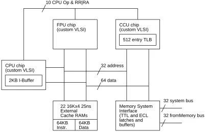
Figure 1 is an overview of one MultiTitan processor. Each processor consists of three custom chips: the CPU, floating point coprocessor (FPU), and external cache controller (CCU).
64 data 32 address
Memory System Interface (TTL and ECL latches and buffers) CCU chip (custom VLSI)
512 entry TLB FPU chip
(custom VLSI)
CPU chip (custom VLSI)
2KB I-Buffer
22 16Kx4 25ns External Cache RAMs
64KB Data 64KB
Instr.
[image:7.612.124.529.52.311.2]32 fromMemory bus 32 system bus
Figure 1: One MultiTitan processor
2.2. Instruction set
The MultiTitan instruction set consists of two instruction formats (see Figure 2). Registers to be fetched in the instruction fetch stage appear in the same place in both formats, so decoding of the format is not required before the access of the register file begins. For example, the register file always fetches the registers specified by the bits in the ra and rb positions, even if the in-struction is in the immediate format. Similarly rr is always accessed in the machine’s last pipes-tage, whether written for ALU operations and loads or read for stores.
A summary of the instruction set is presented in Table 1. The encoding of the instruction fields was chosen to simplify decoding as much as possible. Although the opcode is four bits, many control functions can be determined by examining only a subset of the opcode bits. For example, all instructions in the immediate format have the most significant bit of their opcode equal to 1, while those in the register format have 0 as their most significant bit. All control information is decoded in the instruction fetch stage. Control bits that are used in later pipestages are delayed by shift registers until they are needed. All control signals can be generated by the instruction decode using at most two levels of four-input logic and an inverter. A total of 74 gates are required in all of the instruction decode logic.
3. Implementation
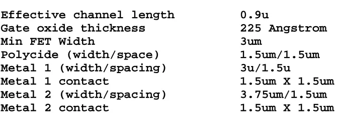
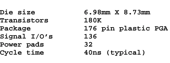
The processor has been implemented in a 1.5u CMOS process. Typical process parameters are given in Table 2. Table 3 summarizes major characteristics of the chip. A photomicrograph of the chip is given in Figure 3.
opcode rr ra rb miscellaneous
Register Format:
Immediate format:
6 10
6 6
4
4 6 6 16
[image:8.612.53.525.359.491.2]opcode rr ra displacement
Figure 2: MultiTitan instruction formats
register format: immediate format:
opcode instruction opcode instruction
0 trap 8 reserved
1 extract 9 test (cop ALU inverse)
2 undefined 10 coprocessor store (64b)
3 variable extract 11 coprocessor load (64b) 4 coprocessor->CPU xfer 12 CPU store
5 CPU->coprocessor xfer 13 CPU load
6 coprocessor ALU 14 conditional jump
7 CPU ALU 15 add immediate
Table 1: Encoding of the primary opcode field
______________________________________________
Effective channel length 0.9u
Gate oxide thickness 225 Angstrom
Min FET Width 3um
Polycide (width/space) 1.5um/1.5um Metal 1 (width/spacing) 3u/1.5u
Metal 1 contact 1.5um X 1.5um
Metal 2 (width/spacing) 3.75um/1.5um
Metal 2 contact 1.5um X 1.5um
[image:8.612.118.454.536.659.2]______________________________________________
Table 2: Process characteristics (as drawn unless specified otherwise)
______________________________________
Die size 6.98mm X 8.73mm Transistors 180K
Package 176 pin plastic PGA Signal I/O’s 136
Power pads 32
Cycle time 40ns (typical)
[image:9.612.155.432.83.186.2]______________________________________
Table 3: Summary of chip characteristics
128 rows and 160 columns, with a cache line size of 16 bytes. The cell is a 6T static cell. Overall access time is 1/2 cycle. The register file consists of 48 32b general purpose registers. The register cell is an 8T static cell with two dual-rail ports. Access time of the register file is 1/4 cycle.
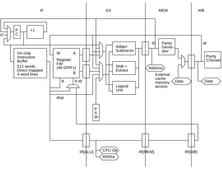
3.1. Pipeline Design
The processor has a four-stage pipeline: instruction fetch (IF), execute (ALU), memory access (MEM), and write back (WB). The resources and timing of the pipeline are shown in Figure 4. During IF, the PC is selected and the instruction is fetched from the direct-mapped on-chip cache. The parity of the instruction is checked, the source registers required by the instruction are fetched, the instruction is decoded, and all (hardware) interlocks are computed in parallel with the instruction cache tag comparison. Note that due to the simple architecture and organiza-tion there is no need for an instrucorganiza-tion decode stage, as is present in most machines. This saves a pipeline stage before the branch determination point in the pipeline, allowing the branch delay to be one cycle instead of two and improving the sustained performance by approximately 10% for a given peak performance.
In the ALU pipestage ALU operations, address calculation of memory access instructions, and branch address calculations are performed. For full performance many machine organizations require separate adders for branch displacements, memory addresses, and ALU operations. Since these calculations are in the same pipestage in this machine, only a single shared adder is required. This increases the utilization of the ALU to about 79% of the instructions executed on a wide range of benchmarks.
In the MEM pipestage memory access instructions send out their address over the 32b address bus at the beginning of the cycle. Load instructions receive their data at the end of the MEM cycle, but the result of the external cache tag comparison is not known until the end of the WB pipestage. The results of all instructions are written to the register file in the WB pipestage. Stores read their data out of the register file during WB as well, so the only difference to the register file between loads, ALU operations, and stores is the R/W control.
Insert die photo with floorplan overlay here.
Unit Transistors %Transistors %Area
I-Cache 134,540 75.0 30.3
Register file 16,516 9.2 5.8
Data path 15,486 8.6 5.7
Control logic 1,757 1.0 2.8
Pads & interface 11,091 6.2 33.7
[image:11.612.140.508.70.162.2]Global routing 14.7
Table 4: CPU transistors and area by unit
A
B IF
Adder/ Subtractor
Shift + Extract
Logical Unit
EX MEM
W Register File (48 GPR’s)
WB
IR[MEM] IR[WB]
IR[ALU]
R Parity Gener-ator +1
On-chip Instruction Buffer 512 words Direct mapped 4 word lines "0"
External cache memory access
P S W
RR|RA CPU Op
Data Address
Data P
C
W
Parity Checker
B A,W
disp
Figure 4: CPU pipeline and machine organization
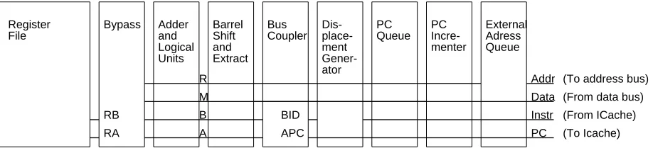
[image:11.612.99.556.199.551.2]lambda also was useful in that it is divisible by many numbers, allowing a wide variety of struc-tures to be efficiently doubled, tripled, or quadrupled up in one datapath pitch.
Data Addr
APC
BID (From ICache)
External Adress Queue
Dis- place-ment Gener-ator
PC A
(To address bus) (From data bus)
(To Icache) Instr
PC Queue
PC Incre-menter
M
RA RB
R
B Register
File
Bus Coupler Barrel
Shift and Extract Adder
[image:12.612.58.517.125.233.2]and Logical Units Bypass
Figure 5: Bus floorplan in the CPU datapth
During the design of the machine we considered a more aggressive pipeline design that split each of the pipestages of Figure 4 into two pipestages. This would double the peak rate (bandwidth) of instruction execution, but the actual time (latency) required for the execution of instructions would not change. Unfortunately, benchmark performance tends to be limited by data dependencies and control dependencies (i.e., branches), so doubling the peak rate without improving the latency of dependencies only resulted in many more stall cycles and decreased utilization of the machine. We simulated a collection of large benchmarks using a parameteriz-able optimizing compilation and simulation system, on both the MultiTitan and the double-pipelined machines [6]. The average sustained performance improvement on a wide range of benchmarks from doubling the number of pipeline stages was only 18%. Given the paucity of the improvement, the increased design effort required for double-pipelining, and the cycle time risk of the extra complexity, we decided to implement a four-stage MultiTitan pipeline.
3.2. Distributed control and decode
One of the interesting aspects of the machine design was its emphasis on distributed decode and control. Figure 6 contrasts distributed and centralized control schemes. The centralized instruction decode and pipeline control is similar to that used in the Stanford MIPS processor [3] as well as typical of other processors. In a centralized decode scheme, signals must typically go from a chip-wide instruction bus through decode or control logic and fan out to the rest of the chip. In this case two chip-width crossings are required in the worst case to generate a control signal. Moreover, on the average the generation of each control signal requires the crossing of the entire chip.
In a distributed control scheme the need for global communication is much reduced. The worst case signal crossing required to generate a signal is one chip-width crossing, but many signals can be generated with almost no global communication (see Figure 6).
Note that simple instruction decode and pipeline control is a prerequisite for distributed con-trol implementations. Machines with complex, interdependent, or irregular concon-trol structures are unlikely to be able to afford distributed control methods.
Distributed decode and control Centralized decode and control
Distributed decode and control
Datapath Instruction Decode
Pipeline Control
[image:13.612.94.553.74.261.2]Datapath
Figure 6: Distributed vs. centralized decode and control
or other large structures are used. Optimizing CAD programs are used to share logic gates be-tween functions within these structures in order to remove redundancy. However, not only are centralized schemes penalized by the wire delay to get to them and to get back to the part of the machine being controlled, but large amounts of area are also required for the routing of these wires. Finally, if PLAs are used to implement centralized control or decode, they are themselves dominated by wire area and wire delay.
In contrast distributed control generally avoids optimization to share logic and eliminate redundancy. For example, in the MultiTitan CPU chip if the same control signal is required at two ends of the data path, the logic to compute the control signal is merely duplicated at both ends of the data path. Not only does duplicating a few gates take up less space than bussing a control signal all the way across a chip, but computing it locally is much faster as well. As another example, instead of putting all the logic into a single large structure (e.g., PLA), small strips of logic gates are placed all along the data path to compute control signals wherever they are needed. The implementation of these logic strips is discussed in section 5.
Even in a distributed control scheme some signals must cross the width of the chip. For ex-ample, if one section of the machine identifies the need to stall, it must be able to communicate this quickly to the rest of the machine. In the MultiTitan CPU we developed a simplified method of global pipeline control. This is aided by the fact that in the MultiTitan all instructions pass through every pipestage and instructions pass through each stage in order.
Typically stalls and interrupts are communicated by a number of signals denoting exceptional conditions (e.g., cache miss, instruction buffer miss, page fault, interlock type x, etc.) These exceptional conditions must be prioritized and translated into control signals for each pipeline stage. Many of the exceptional conditions or interrupts come from distant portions of the machine and may spend a considerable amount of the cycle just traveling to a central prioritizer.
signaled within the CPU by deasserting the LoadX signals required by that exception. When the pipeline control for one pipestage is deasserted, in order to prevent upstream instructions from entering the stalled pipestage, the detector of the exceptional condition must deassert all LoadX control signals for stages previous to X as well. Since all deassertions of a particular LoadX signal are wired-ORed, the net effect will be the same as the exceptional condition that deasserts the most signals, providing the same functionality as a central prioritizer, but in a distributed fashion. (The wired-OR is provided by a precharged node with multiple pull-downs, one for each stall generator.)
Given these LoadX pipeline control signals, the control of the machine is very simple. Many circuits, such as the shift control of the PC queue, connect directly to the pipeline control signals. The most complex use of the pipeline control signals requires a two-input NAND gate and an inverter.
4. Circuits
4.1. Clock
The CPU uses a four phase clocking scheme. The schematic of the clock phase generator is shown in Figure 7. In the nominal case, the phases are derived from the 100 MHz external master clock. An external system reset synchronizes the clocks on all the chips in the system. In practice, the incoming master clock at best looks like a sine wave with noises. To turn the sloppy wave form into sharp edges, a Schmitt trigger receiver is used to receive both the master clock and the system reset. A reset pulse, creset, is generated by a D-FF(D-Flip Flop) and an AND gate. It resets the D-FF’s of the phase generator. The timing of the system reset is not critical. It can either lead or lag the master clock by more than 90 degrees without causing errors. On board delay lines are used for fine tuning.
The clock generator consists of a code counter and a phase generator/driver. The gray-code counter divides the input clock by four and generates Q1(Phi34) and Q2(Phi23) that are offset by 90 degrees. Both true and complement of Q1 and Q2 are then used to generate the desired phases with simple logic. The same clock phase generator is also used in the cache control unit and the floating point unit with only the phase drivers tuned to their respective load-ings. On the CPU, only simple phases are used. Note that in our scheme, only the falling edge of the master clock is used to trigger the phases. Clock skews caused by the imbalance between the rising and falling edges are avoided.
Clock phases are also driven off the chip with near-by pad drivers. Aside from testing pur-poses, they could be used to match the chip set and minimize overall system clock skews. The ultimate matching is to fabricate the chip set on the same wafer to minimize process variations.
4.2. The Register File Sense Amplifier
creset ~clk ~clk
D - FF
r clk ~clk
D Q
~Q
D - FF
r clk ~clk
D Q
~Q
~clk
D - FF
r clk ~clk
D Q
~Q Schmitt
trigger Schmitt trigger
(B) D-Flip Flop
(A) Clock Phase Generator
Q ~Q
clk
~clk D
r system
reset
clk clk
~clk master
clk Q1 ~Q1 Q2 ~Q2
clk clk
phi2 phi3 phi4
phi1 phi13 phi24
clk
~clk
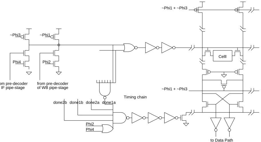
[image:15.612.100.557.81.481.2]Phi1 Phi2 Phi3 Phi4
Figure 7: Schematic of the on-chip clock generator
evaluation phase (phase 2 or 4), the final decoding is done followed by sensing of the bit lines and driving of the datapath busses. Since this all happens within one phase, a timing chain is built to gate the sense amplifier. Four eight-way NANDs are used to generate the "done" signals for the final decoding stage of both ports. The "done" signals are then AND together with the evaluating clock phase followed by an inverter delay chain. The delay chain is tuned such that the sense amplifier is turned on when sufficient differential voltages have developed on the bit lines to guarantee correctness.
to Data Path done1b done2a done1a
done2b ~Phi1 ~Phi3
Phi4 Phi2
Celll
Timing chain from pre-decoder
of IF pipe-stage from pre-decoderof WB pipe-stage
Phi2 Phi4
~Phi1 + ~Phi3
[image:16.612.65.521.84.333.2]~Phi1 + ~Phi3
Figure 8: Schematic of the register file timing chain
4.3. Issues of Ldi/dt and Decoupling Capacitors
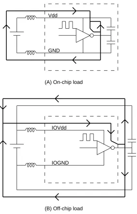
Ldi/dt problems arise mainly from the lead inductance of the chip package. Noises are generated when pad drivers are switched. Internal Vdd and GND are separated from that of the pad drivers to decouple the IO switching noise. Figure 9 shows a simple schematic of an in-verter driving an on-chip (A) and an off-chip (B) capacitor. Dashed lines depict the chip bound-ary and thick lines show the current path. It is obvious that the lead inductances of IOVdd and IOGND cannot be bypassed by either an on-chip or an off-chip decoupling capacitor. Reducing di/dt and/or the package inductances is the only means to cut down the output switching noise. On the other hand, the di/dt generated by the internal circuits can be bypassed through a decou-pling capacitor connected between Vdd and GND.
On the 176-pin PGA that was used, 3 IOVdd and 4 IOGnd are allocated on one side of the chip. These are double-size pads that are doubly bonded to reduce the resistances and induc-tances. In order to minimize the effective number of simultaneously switched drivers, the ad-dress pins and the data pins are interleaved and distributed uniformly along the four sides. With this scheme, the effective number of simultaneously switched drivers is about halved. It is es-timated that the effective inductance one pad driver sees is about 8nH on the IOVdd lead and 7nH on the IOGnd lead. The pad drivers are designed to these parameters with the worse case on-board trace. In the typical case, the simulated chip-crossing delay is about 5.5 ns.
GND Vdd
IOGND IOVdd (A) On-chip load
[image:17.612.187.470.74.513.2](B) Off-chip load
Figure 9: The up-going current path of on-chip and off-chip capacitive loadings
In this simple model, only the chip package inductances, the non-pre-charge type circuitry, e.g. the clock driver, and the pre-charge type circuitry are differentiated. From direct layout extraction, the total capacitance between Vdd and GND comes to about 2000 pF (Cwell ~ 45% and C ~ 55%) and the ratio of Cp gnd to Cvddis > 3. The time constant of a well is given by
2
l rsheet unit_areac , where l is the largest distance from the far point of the well to the well contact, rsheetis the well sheet resistance and cunit areais the well capacitance per unit area. In our CMOS
2
Cp
Cgnd Cvdd Cd_on
pre-charge type circuitry non-pre-charge type circuitry Cd_off
L L M
GND Vdd package chip
Cgnd Cvdd
Cwell eval
[image:18.612.54.520.85.328.2]~prech Rwell
Figure 10: The pre-charge type and non-pre-charge type circuitries.
There’s one very interesting aspect of the pre-charge circuitry. Since pre-charge always takes a full phase, it has a relatively long time constant( > 2 ns). Note also that in the pre-charge phase, the current flows from Vdd through the pre-charge transistors, Cgnd and then to GND. Cvdddischarges through a local loop. In the evaluation phase, Cgnddischarges promptly through a local loop, while only the small Cvddrequires charging current from the power supply. This greatly alleviates the Ldi/dt problem in that the larger capacitance is always switched very slowly (Cgnd/CVdd> 3). Even in the case where CVddand Cgndare comparable, only half of the capacitive loading is subject to fast switching.
Indeed, most of the heavy loadings in the design occur in pre-charge type circuitry. Good examples are the bit lines, the busses, and the domino circuits. Furthermore, in one cycle, only one third of the columns in the instruction cache are active, and different circuits are pre-charged at different phases. Within a phase, the effective capacitive loading that requires current from the power supply is much smaller than the apparent capacitive loading. It is estimated that the capacitances from Cwelland C is about enough to effectively decouple the lead inductances inp the package to ensure a less than 10 percent of the internal power supply variations due to inter-nal di/dt.
5. Design, Verification, and Test Methodology
In the design of the MultiTitan CPU we used a sophisticated yet conservative design methodology. In general the circuit designs were kept simple and regular. The most important advantage of this was that the simple and regular circuits could be fully understood by high-level chip-wide analysis tools. This allowed us to optimize the design as a whole, and saved needless microoptimization of areas which were not critical in the design as a whole. For example, we only used SPICE on six circuits in the machine: the register file sense amp, the instruction cache sense amp, the master clock, pad di/dt, the decoupling capacitor, and the adder carry chain. Even though we did run SPICE on these circuits, they were still relatively simple and could be under-stood by our switch-level simulator and timing verifier. This allowed us to run these tools on the whole chip without having to remove "tricky circuits" that the tools could not understand. This is important because design bugs often result from parts of a chip that are too tricky or too large to be modelled directly, and have to be replaced by simpler circuits in the simulation. This simplified modeling then can easily obscure design problems, especially problems in the inter-face area between the models.
By being able to simulate test vectors directly from the pads of the complete chip during simulation, including the 100MHz AC clock input, we achieved unparalleled confidence in chip functionality. This was validated when we tested the CPU chip on our test board after fab. Once the clock was fed in properly and the rest of the board was debugged, large programs im-mediately began to run without any modification of the object code whatsoever. As of this time no design errors have been found, not even any requiring the "redefinition" of any instruction behavior.
This high-level design approach also was very efficient in terms of design time required. Only 2.5 man-years were required for the design, including all aspects of design from the definition of the instruction set, through the architecture, organization, logic, circuit, layout, and testing.
5.1. Design process overview
The design process was started by prototyping typical circuits (adders, register files, etc.) in the target technology. These initial designs provided data for making architectural and organiza-tional tradeoffs in the machine. Each design was optimized locally (e.g., not all had the same data path pitches), so they were all thrown away when the real logic, circuit, and layout designs were begun.
Next the detailed design of CPU was begun. The Magic layout system [8] was used for the layout editing, design rule checking, and extraction. It was extended locally to check electrical well design rules.
Next a detailed functional-level simulator was written in Modula-2. The functional-level simulator included modules for the CCU and FPU chips as well as the memory system interface. Unfortunately this was not developed until the detailed design of the CPU was nearly complete. A number of changes to the control logic were found to be necessary as a result of the functional simulations in order for the CPU to operate properly in a systems environment when handling interrupts and stalls.
The functional-level simulator was also used to generate test vectors for switch-level simula-tion. The same test cases that were run on the functional-level simulator could then be run on the switch-level simulation of the chip, albeit 1,000 times more slowly. RSIM [14] was used for switch-level simulation. One of the major reasons for choosing it was that it performed timing-based switch-level simulation; this was necessary for circuits like the register file sense amp timing chain.
A much improved version of TV [4] was used for static checking, timing analysis, and clock-ing verification. The static checkclock-ing was used to verify that our simple and regular circuit design methodology was followed. This included the following checks:
•No dynamic nodes driving dynamic nodes through pull-down transistors. (See Figure 11.) This ensured a high margin on dynamic nodes.
•Transitioning coupling capacitance to dynamic nodes resulted in signal deviations within noise margin limits.
•Charge sharing in dynamic structures, such as within evaluating domino blocks, was within noise margin limits.
A
Out
[image:20.612.223.380.460.672.2]Phi Phi
Finally, Ariel [13] was used for power drop simulation of Vdd and GND networks. It per-formed its analysis by extracting the parasitic resistors in the Vdd and GND network. Then it took a trace of switching events from RSIM, and played the current generated from these events across the power network. Based on this power network simulation, several roundabout connec-tions of Vdd and GND to the control logic were rerouted into more direct connecconnec-tions, saving several tenths of a volt drop in the worst case.
5.2. Standard cell implementation of distributed decode and control
As mentioned previously, the decode and control logic of the machine was distributed ad-jacent to its use, and was designed using a standard cell model. We did not have any suitable standard-cell tools available for the design, so since there was only a small number of gates required in total, and the relative placement of the gates was defined by their use in the data path, the layout of the standard cells into layout strips was performed by hand. Part of one of these control strips is given in Figure 12. Because of the simplicity of the instruction encoding, at most two levels of logic and an inverter are required to generate all the decoded instruction con-trol signals in the chip. The two levels of logic and optional inverter correspond to the leftmost three columns, with the inverters in the leftmost column. Because all the instruction decode is performed in the IF pipestage, if control signals are required by later pipestages then they are delayed by the appropriate number of pipestage delay blocks. These delay elements are placed in the the next three columns. Finally, in the rightmost column one additional level of logic is provided for combining the outputs of signals delayed by different amounts.
5.3. Clock tuning with TV
Extensive clock tuning was performed with TV. This tuning consisted of two major aspects: tuning for functionality (i.e., clocking verification), and tuning for performance (i.e., timing analysis).
The performance of the overall design was improved by about 50% through the use of timing analysis. However, this performance improvement is actually the least important implication of the timing analysis. Presumably something very close to the final performance could have been achieved without timing analysis but with large amounts of simulation and careful hand analysis. However, the most important benefit of the timing analysis was the ability to do a simple straightforward circuit design everywhere and to only put in significant design effort at improv-ing performance in the places where it was really necessary in the global framework.
More important than performance is correct functionality. Correct clocking was assured by the clocking verification provided by TV. In clocking verification the set-up and hold times of all the latches and precharged nodes in the machine are verified to have a specified timing mar-gin. Although simulation-based approaches can find some outright set-up or hold violations, they cannot find low margin latches with a practical amount of designer effort.
mcon1.cif scale: 0.005000 (127X) Size: 1576 x 747 microns ( ( ( ( ( ((( ( ( ( ( ( ((( ( ( ( ( ( ( ( ( ( ( ( ( ( ( ( ( ( ( ( ( ( ( ( ( ( ( ( ( ( ( ( ( ( ( ( ( ( ( ( ( ( ( ( ( ( ( ( ( ( ( ( ( ( ( ( ( ( ( ( ( ( ( ( ( ( ( ( ( ( ( ( ( ( ( ( ( ( ( ( ( ( ( ( ( ( ( ( ( ( ( ( ( ( ( ( ( ( ( ( ( ( ( ( ( ( ( ( ( ( ( ( ( ( ( ( ( ( ( ( ( ( ( ( ( ( ( ( ( ( ( ( ( ( ( ( ( ( ( ( ( ( ( ( ( ( ( ( ( ( ( ( ( ( ( ( ( ( ( ( ( ( ( ( ( ( ( ( ( ( ( ( ( ( ( ( ( ( ( ( ( ( ( ( ( ( ( ( ( ( ( ( ( ( ( ( ( ( ( ( ( ( ( ( ( ( ( ( ( ( ( ( ( ( ( ( ( ( ( ( ( ( ( ( ( ( ( ( ( ( ( ( ( ( ( ( ( ( ( ( ( ( ( ( ( ( ( ( ( ( ( ( ( ( ( ( ( ( ( ( ( ( ( ( ( ( ( ( ( ( ( ( ( ( ( ( ( ( ( ( ( ( ( ( ( ( ( ( ( ( ( ( ( ( ( ( ( ( ( ( ( ( ( ( ( ( ( ( ( ( ( ( ( ( ( ( ( ( ( ( ( ( ( ( ( ( ( ( ( ( ( ( ( ( ( ( ( ( ( ( ( ( ( ( ( ( ( ( ( ( ( ( ( ( ( ( ( ( ( ( ( ( ( ( ( ( ( ( ( ( ( ( ( ( ( ( ( ( ( ( ( ( ( ( ( ( ( ( ( ( ( ( ( ( ( ( ( ( ( ( ( ( ( ( ( ( ( ( ( ( ( ( ( ( ( ( ( ( ( ( ( ( ( ( ( ( ( ( ( ( ( ( ( ( ( ( ( ( ( ( ( ( ( ( ( ( ( ( ( ( ( ( ( ( ( ( ( ( ( ( ( ( ( ( ( ( ( ( ( ( ( ( ( ( ( ( ( ( ( ( ( ( ( ( ( ( ( ( ( ( ( ( ( ( ( ( ( ( ( ( ( ( ( ( ( ( ( ( ( ( ( ( ( ( ( ( ( ( ( ( ( ( ( ( ( ( ( ( ( ( ( ( ( ( ( ( ( ( ( ( ( ( ( ( ( ( ( ( ( ( ( ( ( ( ( ( ( ( ( ( ( ( ( ( ( ( ( ( ( (( ( ( ( ( ( ( ( ( ( ( ( ( ( ( ( ( ( ( ( ( ( ( ( ( ( ( ( ( ( ( ( ( ( ( ( ( ( ( ( ( ( ( ( ( ( ( ( ( ( ( ( ( ( ( ( ( ( ( ( ( ( ( ( ( ( ( ( ( ( ( ( ( ( ( ( ( ( ( ( ( ( ( ( ( ( ( ( ( ( ( ( ( ( ( ( ( ( ( ( ( ( ( ( ( ( ( ( ( ( ( ( ( ( ( ( ( ( ( ( ( ( ( ( ( ( ( ( ( ( ( ( ( ( ( ( ( ( ( ( ( ( ( ( ( ( ( ( ( ( ( ( ( ( ( ( ( ( ( ( ( ( ( ( ( ( ( ( ( ( ( ( ( ( ( ( ( ( ( ( ( ( ( ( ( ( ( ( ( ( ( ( ( ( ( ( ( ( ( ( ( ( ( ( ( ( ( ( ( ( ( ( ( ( ( ( ( ( ( ( ( ( ( ( ( ( ( ( ( ( ( ( ( ( ( ( ( ( ( ( ( ( ( ( ( ( ( ( ( ( ( ( ( ( ( ( ( ( ( ( ( ( ( ( ( ( ( ( ( ( ( ( ( ( ( ( ( ( ( ( ( ( ( ( ( ( ( ( ( ( ( ( ( ( ( ( ( ( ( ( ( ( ( ( ( ( ( ( ( ( ( ( ( ( ( ( ( ( ( ( ( ( ( ( ( ( ( ( ( ( ( ( ( ( ( ( ( ( ( ( ( ( ( ( ( ( ( ( ( ( ( ( ( ( ( ( ( ( ( ( ( ( ( ( ( ( ( ( ( ( ( ( ( ( ( ( ( ( ( ( ( ( ( ( ( ( ( ( ( ( ( ( ( ( ( ( ( ( ( ( ( ( ( ( ( ( ( ( ( ( ( ( ( ( ( ( ( ( ( ( ( ( ( ( ( ( ( ( ( ( ( ( ( ( ( ( ( ( ( ( ( ( ( ( ( ( ( ( ( ( ( ( ( ( ( ( ( ( ( ( ( ( ( ( ( ( ( ( ( ( ( ( ( ( ( ( ( ( ( ( ( ( ( ( ( ( ( ( ( ( ( ( ( ( ( ( ( ( ( ( ( ( ( ( ( ( ( ( ( ( ( ( ( ( ( ( ( ( ( ( ( ( ( ( ( ( ( ( ( ( ( ( ( ( ( ( ( ( ( ( ( ( ( ( ( ( ( ( ( ( ( ( ( ( ( ( ( ( ( ( ( ( ( ( ( ( ( ( ( ( ( ( ( ( ( ( ( ( ( ( ( ( ( ( ( ( ( ( ( ( ( ( ( ( ( ( ( ( ( ( ( ( ( ( ( ( ( ( ( ( ( ( ( ( ( ( ( ( ( ( ( ( ( ( ( ( ( ( ( ( ( ( ( ( ( ( ( ( ( ( ( ( ( ( ( ( ( ( ( ( ( ( ( ( ( ( ( ( ( ( ( ( ( ( ( ( ( ( ( ( ( ( ( ( ( ( ( ( ( ( ( ( ( ( ( ( ( ( ( ( ( ( ( ( ( ( ( ( ( ( ( ( ( ( ( ( ( ( ( ( ( ( ( ( ( ( ( ( ( ( ( ( ( ( ( ( ( ( ( ( ( ( ( ( ( ( ( ( ( ( ( ( ( ( ( ( ( ( ( ( ( ( ( ( ( ( ( ( ( ( ( ( ( ( ( ( ( ( ( ( ( ( ( ( ( ( ( ( ( ( ( ( ( ( ( ( ( ( ( ( ( ( ( ( ( ( ( ( ( ( ( ( ( ( ( ( ( ( ( ( ( ( ( ( ( ( ( ( ( ( ( ( ( ( ( ( ( ( ( ( ( ( ( ( ( ( ( ( ( ( ( ( ( ( ( ( ( ( ( ( ( ( ( ( ( ( ( ( ( ( ( ( ( ( ( ( ( ( ( ( ( ( ( ( ( ( ( ( ( ( ( ( ( ( ( ( ( ( ( ( ( ( ( ( ( ( ( ( ( ( ( ( ( ( ( ( ( ( ( ( ( ( ( ( ( ( ( ( ( ( ( ( ( ( ( ( ( ( ( ( ( ( ( ( ( ( ( ( ( ( ( ( ( ( ( ( ( ( ( ( ( ( ( ( ( ( ( ( ( ( ( ( ( ( ( ( ( ( ( ( ( ( ( ( ( ( ( ( ( ( ( ( ( ( ( ( ( ( ( ( ( ( ( ( ( ( ( ( ( ( ( ( ( ( ( ( ( ( ( ( ( ( ( ( ( ( ( ( ( ( ( ( ( ( ( ( ( ( ( ( ( ( ( ( ( ( ( ( ( ( ( ( ( ( ( ( ( ( ( ( ( ( ( ( ( ( ( ( ( ( ( ( ( ( ( ( ( ( ( ( ( ( ( ( ( ( ( ( ( ( ( ( ( ( ( ( ( ( ( ( ( ( ( ( ( ( ( ( ( ( ( ( ( ( ( ( ( ( ( ( ( ( ( ( ( ( ( ( ( ( ( ( ( ( (( ( ( ( ( ( ( ( ( ( ( ( ( ( ( ( ( ( ( ( ( ( ( ( ( ( ( ( ( ( ( ( ( ( ( ( ( ( ( ( ( ( ( ( ( ( ( ( ( ( ( ( ( ( ( ( ( ( ( ( ( ( ( ( ( ( ( ( ( ( ( ( ( ( ( ( ( ( ( ( ( ( ( ( ( ( ( ( ( ( ( ( ( ( ( ( ( ( ( ( ( ( ( ( ( ( ( ( ( ( ( ( ( ( ( ( ( ( ( ( ( ( ( ( ( ( ( ( ( ( ( ( ( ( ( ( ( ( ( ( ( ( ( ( ( ( ( ( ( ( ( ( ( ( ( ( ( ( ( ( ( ( ( ( ( ( ( ( ( ( ( ( ( ( ( ( ( ( ( ( ( ( ( ( ( ( ( ( ( ( ( ( ( ( ( ( ( ( ( ( ( ( ( ( ( ( ( ( ( ( ( ( ( ( ( ( ( ( ( ( ( ( ( ( ( ( ( ( (( (( ( (( (( (( (( ( ( ( ( ( ( ( ( ( ( ( ( ( ( ( ( ( ( ( ( ( ( ( ( ( ( ( ( ( ( ( ( ( ( ( ( ( ( ( ( ( ( ( ( ( ( ( ( ( ( ( ( ( ( ( ( ( ( ( ( ( ( ( ( ( ( ( ( ( ( ( ( ( ( ( ( ( ( ( ( ( ( ( ( ( ( ( ( ( ( ( ( ( ( ( ( ( ( ( ( ( ( ( ( ( ( ( ( ( ( ( ( ( ( ( ( ( ( ( ( ( ( ( ( ( ( ( ( ( ( ( ( ( ( ( ( ( ( ( ( ( ( ( ( ( ( ( ( ( ( ( ( ( ( ( ( ( ( ( ( ( ( ( ( ( ( ( ( ( ( ( ( ( ( ( ( ( ( ( ( ( ( ( ( ( ( ( ( ( ( ( ( ( ( ( ( ( ( ( ( ( ( ( ( ( ( ( ( ( ( ( ( ( ( ( ( ( ( ( ( ( ( ( ( ( ( ( ( ( ( ( ( ( ( ( ( ( ( ( ( ( ( ( ( ( ( ( ( ( ( ( ( ( ( ( ( ( ( ( ( ( ( ( ( ( ( ( ( ( ( ( ( ( ( ( ( ( ( ( ( ( ( ( ( ( ( ( ( ( ( ( ( ( ( ( ( ( ( ( ( ( ( ( ( ( ( ( ( ( ( ( ( ( ( ( ( ( ( ( ( ( ( ( ( ( ( ( ( ( ( ( ( ( ( ( ( ( ( ( ( ( ( ( ( ( ( ( ( ( ( ( ( ( ( ( ( ( ( ( ( ( ( ( ( ( ( ( ( ( ( ( ( ( ( ( ( ( ( ( ( ( ( ( ( ( ( ( ( ( ( ( ( ( ( ( ( ( ( ( ( ( ( ( ( ( ( ( ( ( ( ( ( ( ( ( ( ( ( ( ( ( ( ( ( ( ( ( ( ( ( ( ( ( ( ( ( ( ( ( ( ( ( ( ( ( ( ( ( ( ( ( ( ( ( ( ( ( ( ( ( ( ( ( ( ( ( ( ( ( ( ( ( ( ( ( ( ( ( ( ( ( ( ( ( ( ( ( ( ( ( ( ( ( ( ( ( ( ( ( ( ( ( ( ( ( ( ( ( ( ( ( ( ( ( ( ( ( ( ( ( ( ( ( ( ( ( ( ( ( ( ( ( ( ( ( ( ( ( ( ( ( ( ( ( ( ( ( ( ( ( ( ( ( ( ( ( ( ( ( ( ( ( ( ( ( ( ( ( ( ( ( ( ( ( ( ( ( ( ( ( ( ( ( ( ( ( ( ( ( ( ( ( ( ( ( ( ( ( ( ( ( ( ( ( ( ( ( ( ( ( ( ( ( ( ( ( ( ( ( ( ( ( ( ( ( ( ( ( ( ( ( ( ( ( ( ( ( ( ( ( ( ( ( ( ( ( ( ( ( ( ( ( ( ( ( ( ( ( ( ( ( ( ( ( ( ( ( ( ( ( ( ( ( ( ( ( ( ( ( ( ( ( ( ( ( ( ( ( ( ( ( ( ( ( ( ( ( ( ( ( ( ( ( ( ( ( ( ( ( ( ( ( ( ( ( ( ( ( ( ( ( ( ( ( ( ( ( ( ( ( ( ( ( ( ( ( ( ( ( ( ( ( ( ( ( ( ( ( ( ( ( ( ( ( ( ( ( ( ( ( ( ( ( ( ( ( ( ( ( (( ( ( ( ( ( ( ( ( ( ( ( ( ( ( ( ( ( ( ( ( ((( ( ( ( ( ( ( ( ( ( ( ( ( ( ( ( ( ( ( ( ( ( ( ( ( ( ( ( ( ( ( ( ( ( ( ( ( ( ( ( 2 2 2 2 2 2 22 2 2 2 2 2222 2 2 2 2 2 2 2 2 2 2 2 2 2 2 2 2 2 2 2 2 2 2 2 2 2 2 2 2 2 2 2 2 2 2 2 2 2 2 2 2 2 2 2 2 2 2 2 2 2 2 2 2 2 2 2 2 2 2 2 2 2 2 2 2 2 2 2 2 2 2 2 2 2 2 2 2 2 2 2 2 222 222 2222 22 222222222
2 22 2 2222 2 2222222222
22 222222222 222222222 2222222222 22222222222222 2222222222 22222222222222222222222222222
222222222 222222222 2222222222222222222222 22222 22 2 2 22222
2 2 2222 2 22 22 22 22 22 22 22 22 22 22 22 22 22 22 22 22 22 22 22 22 22 22 22 22 22 22 22 22 22 22 22 22 22 22222 2 2 2 2 2 2 2 2 2 2 2 2 2 2 2 2 2 2 2 2 2 2 2 2 2 2 2 2 2 2 2 2 2 2 222222 2 2 2 2 2 2 2 2 2 2 2 2 2 2 2 2 2 2 2 2 2 2 2 2 2 2 2 2 2 2 2 2 2 2 2 2 2
2222222222222 22 2222222 22 22222 22 22 22222 222 222 22 22 22 22 222222222
22 22 22222222222222
22 22 222222 22 22 22 22 22 222222222 22222222222222 22222222222222 22222 22 2 22 22222222 222222222 22222 22 22 22 22 222 22 22 222 22222222
22 22222222
2 2 2 2 2 2 2 2 2 2 2 2 2 2 2 2 2 2 2 2 2 2 2 2 2 2 2 2 2 2 2 2 2 2 2 2 2 2 2 2 2 2 2 2 2 2 2 2 2 2 2 2 2 2 2 2 2 2 2 2 2 2 2 2 2 2 2 2 2 2 2 2 2 2 2 2 2 2 2 2 2 2 2 2 2 2 2 2 2 2 2 2 2 2 2 2 2 2 2 2 2 2 2 2 2 2 2 2 2 2 2 2 2 2 2 2 2 22 2 2 2 2 2 2 2 2 2 22 2 2 22 2 2 2 2 2 2 2 2 2 2 2 2 2 2 2 2 2 2 2 2 2 2 2 2 2 2 2 2 2 2 2 2 2 2 2 2 2 2 2 2 2 2 2 2 2 2 2 2 2 2 222 222 222 222 222 222 2 2 2 2 2 2 2 2 2 2 2 2 2 22 2 2 2 2 2 2 2 2 2 2 2 2 2 2 2 2 2 2 2 2 2 2 2 2 2 2 2 2 2 2 2 2 2 22 2 2 2 2 2 2 2 2 2 2 2 2 2 2 22 22 2 22 222 2 22 2 2 22 22 2 22 222 2 22 2 22 2 22 2 2 2 2 2 2 2 2 22 22 22 2 2 2 2 2 2 2 2 2 2 22 22 22 22 22 22 22 22 2222 22 22 22 22 22 222222 22 22 22 2222 2 2 2 2 2 2 2 2 2 2 2 2 2 22 22 2 2 2 2 2 2 2 2 2 2 2 2 2 2 2 2 2 2 2 2 2 222222 2 2 2 2 2 2 222 222222222
2 2 2 2 2222222222
222 2 2 22 22 2222 2 2 22 222222 2 2 222 2 222 2 2222222 222222222 2 2 2 2 2 2 2 2 2 2 2 2 2 2 2 2 2 2 2 2 2 2 2 2 2 2 2 2 2 2 2 2 2 2 2 2 2 2 2 2 2 2 2 2 2 2 2 2 2 2 2 2 2 2 2 2 2 2 2 2 2 2 2 2 2 2 2 2 2 2 2 2 2 2 2 2 2 2 2 2 2 2 2 2 2 2 2 2 2 2 2 2 2 2 2 22 2 2 2 2 2 2 2 2 2 2 2 2 2 2 2 2 2 2 2 2 2 2 2 2 2 2 2 2 2 2 2 2 2 2 2 2 2 2 2 2 2 2 2 2 2 2 2 2 2 2 2 2 2 2 2 2 2 2 2 2 2 2 2 2 2 2 2 2 2 2 2 2 2 2 2 2 2 2 2 2 2 2 2 2 2 2 2 2 2 2 2 2 2 2 2 22 2 2 2 2 2 2 2 2 2 2 2 2 2 2 2 2 2 2 2 2 2 2 2 2 2 2 2 2 2 2 2 2 2 22 22 22 222 22 22222 22 22 22 22 222222222222 2 22 2 22 22 2 2 2 2 2 2 2 2 2 2 2 2 2 2 2 2 2 2 2 2 2 2 2 2 2 2 2 2 2 2 2 2 222222222222 22 22 222 222 2 2 2222 22 22 22 22 2 2 2 222 2 2 2 2 2 2 222 222 2 2 2 2 2 2 2 2 2 2 2 2 2 2 2 2 2222 2 22 2 2 2 2 2 2 2 22 2 22222 22 22 2222 22 2 2 2 2 2 2 2 2 2 2 2 2 2 2 2 2 2 2 2 2 2 2 2 2 2 2 2 2 2 2 2 2 2 2 2 2 2 2 2 2 2 2 2 2 2 2 2 2 2 2 2 2 2 2 2 2 2 2 2 2 2 2 2 2 2 2 2 2 2 2 2 2 2 2 2 2 2 2 2 2 2 2 2 2 2 2 2 2 2 2 2 2 2 2 2 2 2 2 2 2 2 2 2 2 2 2 2 2 2 2 2 2 2 2 2 2 2 2 2 2 2 2 2 2 2 2 2 2 2 2 2 2 2 2 2 2 2 2 2 2 2 2 2 2 2 2 2 2 2 2 2 2 2 2 2 2 2 2 2 2 2 2 2 2 2 2 2 2 2 2 2 2 2 2 2 2 2 2 2 2 2 2 2 2 2 2 2 2 2 2 2 2 2 2 2 2 2 2 2 2 2 2 2 2 2 2 2 2 2 2 2 2 2 2 2 2 2 2 2 2 2 2 2 2 2 2 2 2 2 2 2 2 2 2 2 2 2 2 2 2 2 2 2 2 2 2 2 2 2 2 2 2 2 2 2 2 2 2 2 2 2 2 2 2 2 2 2 2 2 2 2 2 2 2 2 2 2 2 22 2 2 2 2 22 2 2 22 22 22 22 22 22 22 22 22 2 2 2 2 2 2 2 2 2 2 2 2 2 2 2 2 2 2 2 2 2 2 2 2 2 2 2 2 2 2 2 2 2 2 2 2 2 2 2 2 2 2 2 2 2 2 2 2 2 2 2 2 2 2 2 2 2 2 2 2 2 2 2 2 2 222 2 2 2 2 2 2 2 2 2 2 2 2 2 2 2 2 2 2 2 2 2 2 2 2 2 2 2 2 2 2 2 2 2 2 2 2 2 2 2 22 2 22 2 2 2 2 2 2 2 2 2 22 22 22 2 2 2 2 2 2 2 2 2 2 2 2 2 2 2 2 2 2 2 2 2 2 2 2 2 2 2 2 2 2 2 2 2 2 2 2 2 2 2 2 2 2 2 2 22 2 22 2 2 2 2 2 2 2 2 2 22 2 2 22 2 2 2 222 22 22 22 22 22 22 22 22 22 22 22 2 2 2 2 2 2 2 2 2 2 2 2 2 2222 2222 2222 2222 2 2 2 2 2 2 2 2 2 2 2 2 2 2 2 2 2 2 2 2 2 2 2222 2 2 2 2 2 2 2 2 2 2 2 2 2 2 2 2 2 2 2 2 2 2 2222 22 22 22 22 22 22 22 22 22 22 22 2 2 2 2 2 2 2 2 22222 2 2 2 2 2 2 2 2 2 2 2 2 2 2 2 2 2 2 2 2 2 2 2 2 2 2 2 2 2 2 2 2 2 2 2 2 22222222222222 2 2 2 2 2 22222222222222 2 2 2 2 2 2 2 2 2 2 2 2 2 2 2 2 2 2 2 2 2 2 22222222222222 2 2 2 2 2 2 2 2 2 2 2 2 2 2 2 2 2 2 2 2 2 2 222222222222222 2 2 2 2 2 2 2 2 2 2 2 2 2 2 2 2 2 2 2 2 2 2 2 2 2222 2 2 2 2 2 2 22 22 2 2 2 22 2 2 2 2 2 2 2 2 22 2222 2 2 2 2 2 2 2 2 2 2 2 2 2 2 2222222222222222222 2 2 2 2 2222222 22 22 22 22 2 2 2 2 2 2222222222 22 22 22 2 2 2 2 2 2 2 2 2 2 2 2 222222222222 22222222222222222222 2 2 2 2 2 2 2 2 2 2 2 2 2 2 2 2 2 2 2 2 2 2 2 2 2 2222 2222 2 2 2 2222222222222 2222222222222 2 2 2 2 2 2 2 22 22 22 22 2 2 2 2222 2222 2 2 2 2 2 2 2 2 2 2 2 2 2 2 2 2 2 2 2 2 2 2 2 2 2 22222 2 2 2 2 2 22 22 2 2 2 2 2 2 2 2 2 2 2 2 2 2 2 2 2 2 2 2 2 2 2 2 2 2 2 2222 2 2 2 2 2 2 2 2 2 2 2 2 2 2 2 2 2 2 2 2 2 2 2 2 2 2 22 2 2 2 2 2 2 2 2 2 2 2 2 2 2 2 2 2 2 2 2 2 2 2 2 2 2 2 2 2 2 2 2 2222222 2 2 2 2 2 2 2 2 2 2 2 2 2 2 2 2 2 2 2 2 2 2 2 2 2 2 2 2 2 2 2 2 2 2 2 2 2 2 2 2 2 2 2 2 2 2 2 2 2 2 2 2 2 2 2 2 2 2 2 2 2 2 2 2 2 2 2 2 2 2 2 2 2 2 2 2 2 2 2 2 2 2 2 2 2 2 2 2 2 2 2 2 2 2 2 2 2 2 2 2 2 2 2 2 2 2 2222222 2 22 2 22 2 22 2 2 2 2 2 2 2 2 2 2 2 2 2 2 2 2 2 2 2 2 2 2 2 2 2 2 2 2 2 2 2 2 2 2 2 2 2 2 2 2 2 2 2 2 2 2 2 2 2 22 2 2 2 2 2 2 2 2 2 2 2 2 2 2 2 22 2222 2 22 22 22 22 22 22 22 22 22 2 2 2 2 2 2 22 22 22 22 2 2 2 2 2 2 2 2 2 2 2 2 2 2 2 2 2 2 2 2 2 2 2 2 2 2 2 2 2 2222 2 2 2 2 2 2 2 2 2 2 2 2 2 2 2 2 2 2 2 2 2 2 2 2 2 2 222 2 222 2 222 2 2 2 2 2 2 2 2 2 2 2 2 2 2 2 2 2 2 2 2 2 2 2 2 2 2 2 2 2 2 2 2 2 2 2 2 2 2 2 2 2 2 2 2 2 2 2 2 2 2 2 2 2 2 2 2 2 2 2 2 2 2 2 2 2 2 2 2 2 2 22 2 22 222 2 2 2 2 2 2 2 2 2 2 2 2 2 2 2 2 2 2 2 2 2 2 2 2 2 2 22 2 2 2 2 2 2222 2222 22 22 22 22 22 22 22 22 22 2 2 2 22 22 22 22 2 2 2 2 2 2 2 2 2 2 2 2 2 2 2 2 2 2 2 2 2 2 2 22222222222 2 2 2 2 2 2 2 2 2 2 2 2 2 2 2 2 2 2 2 2 2 2 2 2 2 2 2 2 2 2 2 2 2 2 2 2 22 2 22 2 2 2 2 2 2 2 2 2222222222
22222222222222 2 2 2 2 2 2 2 2 2 2 2 2 2 2 2 2 2 2 2 2 2 2 2 2 2 2 2 2 2 2 2 2 2 2 2 2 2 222222222222222 2 2 2 2 2 2 2 2 2 222222222222222 2 2 2 2 2 2 2 2 22222 2 2 2 2 2 2 2 2 2 2 2 2 22 2 2 222222222222222 22 2 2 22 2 22 22 22 222222222 2 2 22 222222222222222 2 2 2 2222222222222 2 2 2 2 2 2 2 2 2222222222222222 2 2 2
2222222222222222 2222 2222 2222 2 2 2 2 2 2 2 2 2 222 222 2 2 2 2222222222222222222 2 2 2 222 222 222 2 2 2 2 2 22 2 2 2 2 2 2 2222 2 2 2 2222 2 2 2 222 2222 222222222 2 2 2 22 22222222222 222 222 2 2 2 2 2 2 2 2 22222222222 2 2 2 222222222222 22222 2 2 2 2 2 2 2 2 2222222 22222222 2222222222222 2 2222222 222222222 2 2 2 2 2 22222222222222 2222222222222 2 2 222 222 22222222222 2 2 2 22222222222222 2 2 2 2 2 2 22222222222222 222222222 22222 2 2 2 2 2 2 222222222 2 2 2 2 2 2 22222222222222 22222222 22222222222222 2 2 2222 22222222222222 2 2 2 2 2 2 2 2 2 2 2 2 22222222 222222222222222 22222222222222 22222 222222 22222222222222 2 22222 2 2 2 2 2 22 2 2 22222222222 2222222 22222 22222222 2 2 2 2 2 22222222222 22222 22222222222 2 222222 2 2 2 22222 222222222222 22222222 222 22222 22222222222 22222 22 22 2 222222222222222 22 22222222 222222222222222222222222222222222222222
2222222 22 222 2 22 2 222222 2 22 22222222 < < < < < < < < < < < < < < < < < < < < < < < < < < < < < < < < < < < < < < < < < < < < < < < < < < < < < < < < < < < < < < < < < < < < < < < < < < < < < < < < < < < < < < < < < < < < < < < < < < < < < < < < < < < < < < < < < < < < < < < < < < < < < < < < < < < < < < < < < < < < < < < < < < < < < < < < < < < < < < < < < < < < < < < < < < < < < < < < < < < < < < < < < < < < < < < < < < < < < < < < < < < < < < < < < < < < < < < < < < < < < < < < < < < < < < < < < < < < < < < < < < < < < < < < < < < < < < < < < < < < < < < < < < < < < < < < < < < < < < < < < < < < < < < < < < < < < < < < < < < < < < < < < < < < < < < < < < < < < < < < < < < < < < < < < < < < < < < < < < < < < < < < < < < < < < < < < < < < < < < < < < < < < < < < < < < < < < < < < < < < < < < < < < < < < < < < < < < < < < < < < < < < < < < < < < < < < < < < < < < < < < < < < < < < < < < < < < < < < < < < < < < < < < < < < < < < < < < < < < < < < < < < < < < < < < < < < < < < < < < < < < < < < < < < < < < < < < < < < < < < < < < < < < < < < < < < < < < < < < mn mn mn mn mn mn mn mn mn mn mn mn mn mn mn mn mn mn mn mn mn mn mn mn mn mn mn mn mn mn mn mn mn mn mna mn mn mn mn mn mn mn mn mn mn mn mn mn mn mn mn mn mn mn mn mn mn mn mn mn mn mn mn mn mn mn mn mn mn mn mn mn mn mn mn mn mn mn mna mn mn mn mn mn mn mna mna mn mn mn mn mn mn mn mn mna mn mn memfrr GN old inhold_q1 advance_q1
GNDmidVdd hi4 phi3 phi3-memsrr TV:In$ hold advanc GND V mid inout ph hi3 hi memsrr TV:In$ hold advanc GND V mid inout ph hi3 hi memsrr TV:In$advanchold
GNDmidV in out h phi3 phi memfrr GN old in hold q1 advance q1 GND Vdd mid phi4-hi3 phi4-hi3 memsrr TV:In$advanchold
GND V mid in out h phi3 phi memfrr GN old in hold q1 advance q1 GND Vdd mid phi4-hi3 phi4-hi3 memfrr GN old inhold_q1 advance_q1 GND Vdd mid hi4 phi3 phi3-memfrr GN old in hold q1 advance q1 GND Vdd mid phi4-hi3 phi4-hi3 memfrr GN old inhold_q1 advance_q1 GND Vdd mid hi4 phi3 phi3-memfrr GN old in hold q1 advance q1 GND Vdd mid phi4-hi3 phi4-hi3 memfrr GN old inhold_q1 advance_q1 GND Vdd mid hi4 phi3 phi3-memfrr GN old in hold q1 advance q1 GND Vdd mid phi4-hi3 phi4-hi3 memfrr GN old inhold_q1 advance_q1 GND Vdd mid hi4 phi3 phi3-memfrr GN old in hold q1 advance q1 GND Vdd mid phi4-hi3 phi4-hi3 memsrr TV:In$advanchold
GNDmidV in
out h
phi3 phi memsrr TV:In$advanchold
GNDmidV in out h phi3 phi memsrrpair memsrr TV:In$advanchold
GNDmidV in out h phi3 phi mn mn mn mn memsrr TV:In$advanchold
GND V mid in out h phi3 phi memsrr TV:In$advanchold
GNDmidV in
out h
phi3 phi memsrr TV:In$advanchold
GNDmidV in out h phi3 phi memsrrpair memsrr TV:In$ hold advanc GND V mid inout ph hi3 hi memsrr TV:In$ hold advanc GND V mid inout ph hi3 hi memsrrpair memsrr TV:In$ hold advanc GND V mid inout ph hi3 hi memsrr TV:In$ hold advanc GND V mid inout ph hi3 hi memsrrpair memfrr GN old inhold_q1 advance_q1 GND Vdd mid hi4 phi3 phi3-memfrr GN old in hold q1 advance q1 GND Vdd mid phi4-hi3 phi4-hi3 memfrr GN old inhold_q1 advance_q1 GND Vdd mid hi4 phi3 phi3-memfrr GN old in hold q1 advance q1 GND Vdd mid phi4-hi3 phi4-hi3 memfrr GN old inhold_q1 advance_q1
GNDmidVdd hi4 phi3 phi3-memfrr GN old in hold q1 advance q1 GND Vdd mid phi4-hi3 phi4-hi3 memfrr GN old inhold_q1 advance_q1
GNDmidVdd hi4 phi3 phi3-memfrr GN old in hold q1 advance q1 GND Vdd mid phi4-hi3 phi4-hi3 memfrr GN old inhold_q1 advance_q1 GND Vdd mid hi4 phi3 phi3-memsrr TV:In$ hold advanc GND V mid inout ph hi3 hi mn latemux In_hold In_adv memsrr TV:In$ hold advanc GND V mid inout ph hi3 hi mn latemux In_hold In_adv latemux In_hold In_adv memsrr TV:In$ hold advanc GND V mid inout ph hi3 hi memfrr GN old inhold_q1 advance_q1 GND Vdd mid hi4 phi3 phi3-mn mn memfrr GN old inhold_q1 advance_q1 GND Vdd mid hi4 phi3 phi3-memfrr GN old in hold q1 advance q1 GND Vdd mid phi4-hi3 phi4-hi3 memfrr GN old inhold_q1 advance_q1
GNDmidVdd hi4 phi3 phi3-mcon1 SoftTrapInWB WBV-WBValid store SoftTrap- AddOut-Cin lit-active_B<-W active_A<-W BSrc BWBbypAWBbypBMEMbypAMEMbyp
Load_Interlock_B Load_Interlock_A Sub- LUOut- CPUload- Rr=Rb- Rr=Ra- ValidRb- ValidRa-A AW AR CmpOut-lit load BW BB BR load-Litls Litm AL AA
buffer sections were added in parallel to the already existing buffers for signals which needed to be advanced in time to improve margins. For signals which needed to be slowed down, buffer sections were removed or a pair of minimum size buffers were added in series with the control signal. The net result was that several nanoseconds of overlap between adjacent clock phases could be safely tolerated by the chip, even with a 10ns target time per phase.
6. Performance
The CPU was sent out for fabrication in October 1987 and one lot came back in April 1988. The chip was designed for typical operation with a 40ns cycle time and a 100Mhz clock. The CPU was tested on an evaluation board with 512KB of fast RAM. This board resided on the I/O bus of our ECL Titan computer. The maximum operating frequency of the parts returned ranged from 70Mhz to 90Mhz. This performance was consistent with slower than typical processing parameters. At their maximum operating frequency large programs ran on the CPU chip without modification of their object code. At frequencies even slightly above this (e.g., <10%), even the shortest test cases stopped working. Since the chip was tuned with TV so that everything was of similar criticality, having everything fail at about the same point is a confirmation of the tuning performed with TV.
The average contribution of various factors to the simulated system CPI when executing the C compiler, yacc, Livermore loops (scalar code), Linpack (scalar), whetstones, and the Hennessy Stanford benchmarks is given in Table 5. (This data is for simulated system performance, since the evaulation board did not contain the FPU and CCU chips.) Combined with the performance data, this yields a projected sustained system performance of 18 MIPS. It is expected that with typical processing 20 sustained MIPS in a system environment will be achieved.
Cycle CPI
Contribution penalty burden
Normal instruction issue 1 1.000
NOP instructions 1 0.024
On-chip I-cache misses 2 0.032
Load interlocks 1 0.064
Store and transfer interlocks 1 0.074
Wait for result of *,/, and FP varies 0.056 External 128KB direct-mapped
32B line cache misses 10 0.023
[image:23.612.134.510.419.561.2]Total 1.273
Table 5: Sustained average cycles per instruction
7. Summary
8. Acknowledgements
David Boggs designed the CPU evaluation board and produced the speed test results. Bob Alverson, Scott Nettles, and Don Stark provided CAD tools instrumental in the design of the CPU. Jeremy Dion developed the functional simulator of the CPU. David Wall provided the retargetable compilation and instruction-level simulation system used in architecture studies. Leon Yang, Mark Johnson, Bruce Wooley, and the reviewers provided valuable comments on an early draft of this paper.
References
[1] Dobberpuhl, D., et. al.
A 32b Microprocessor with On-Chip Virtual Memory Management.
In The 1984 International Solid-State Circuits Conference, pages 178-179. IEEE Solid State Circuits Council and the University of Pennsylvania, February, 1984.
[2] Fisher, A., et.al.
CMOS Implementation of a 32b Computer.
In The 1989 International Solid-State Circuits Conference, pages 80-81. IEEE Solid State Circuits Council and the University of Pennsylvania, February, 1989.
[3] Hennessy, J. L., Jouppi, N. P., Przybylski, S., Rowen, C., and Gross, T. Design of a High Performance VLSI Processor.
In Bryant, Randal (editor), Third Caltech Conference on VLSI, pages 33-54. Computer Science Press, March, 1983.
[4] Jouppi, Norman P.
Timing Analysis and Performance Improvement of MOS VLSI Designs. In IEEE Transactions on CAD, pages 650-665. July, 1987.
[5] Jouppi, Norman P., Dion, Jeremy, Boggs, David, and Nielsen, Michael J. K. MultiTitan: Four Architecture Papers.
Technical Report 87/8, Digital Equipment Corporation Western Research Lab, April, 1988.
[6] Jouppi, Norman P., Wall, David W.
Instruction-Level Parallelism for Superscalar and Superpipelined Machines.
In The Third Symposium on Architectural Support for Programming Languages and Operating Systems, pages 272-282. IEEE, April, 1989.
[7] Nielsen, M. J. K. Titan System Manual.
Technical Report 86/1, Digital Equipment Corporation Western Research Lab, Septem-ber, 1986.
[8] Ousterhout, John K., Hamachi, Gordon T., Mayo, Robert N., Scott, Walter S., and Taylor, George S.
The Magic Layout System.
[9] Perry, Tekla S. Intel’s Secret is Out.
Spectrum :22-28, April, 1989.
[10] Rowen, C., et. al.
RISC VLSI Design for System-Level Performance. VLSI Systems Design :81-88, March, 1986.
[11] Rubenfeld, P., et. al.
A 32b Microprocessor with On-chip Instruction and Data Caching and Memory Manage-ment.
In The 1987 International Solid-State Circuits Conference, pages 32-33. IEEE Solid State Circuits Council and the University of Pennsylvania, February, 1987.
[12] Sachs, H., and Hollingsworth, W.
A High Performance 846,000 Transistor Unix Engine: The Fairchild Clipper.
In Proceedings IEEE International Conference on Computer Design: VLSI in Computers, pages 342-346. IEEE Computer Society Press, October, 1985.
[13] Stark, Don, and Horowitz, Mark.
Analyzing CMOS Power Supply Networks using Ariel.
In The Proceedings of the 25th Design Automation Conference, pages 460-464. IEEE/ACM, June, 1988.
[14] Terman, C. J.
Simulation Tools for Digital LSI Design.
PhD thesis, MIT Department of Electrical Engineering and Computer Science, 1983.
[15] Wall, David W., and Powell, Michael L.
The Mahler Experience: Using an Intermediate Language as the Machine Description. In Second International Conference on Architectural Support for Programming
WRL Research Reports
‘‘Titan System Manual.’’ ‘‘MultiTitan: Four Architecture Papers.’’
Michael J. K. Nielsen. Norman P. Jouppi, Jeremy Dion, David Boggs, Mich-WRL Research Report 86/1, September 1986. ael J. K. Nielsen.
WRL Research Report 87/8, April 1988. ‘‘Global Register Allocation at Link Time.’’
David W. Wall. ‘‘Fast Printed Circuit Board Routing.’’ WRL Research Report 86/3, October 1986. Jeremy Dion.
WRL Research Report 88/1, March 1988. ‘‘Optimal Finned Heat Sinks.’’
William R. Hamburgen. ‘‘Compacting Garbage Collection with Ambiguous WRL Research Report 86/4, October 1986. Roots.’’
Joel F. Bartlett.
‘‘The Mahler Experience: Using an Intermediate WRL Research Report 88/2, February 1988. Language as the Machine Description.’’
David W. Wall and Michael L. Powell. ‘‘The Experimental Literature of The Internet: An WRL Research Report 87/1, August 1987. Annotated Bibliography.’’
Jeffrey C. Mogul.
‘‘The Packet Filter: An Efficient Mechanism for WRL Research Report 88/3, August 1988. User-level Network Code.’’
Jeffrey C. Mogul, Richard F. Rashid, Michael ‘‘Measured Capacity of an Ethernet: Myths and
J. Accetta. Reality.’’
WRL Research Report 87/2, November 1987. David R. Boggs, Jeffrey C. Mogul, Christopher A. Kent.
‘‘Fragmentation Considered Harmful.’’ WRL Research Report 88/4, September 1988. Christopher A. Kent, Jeffrey C. Mogul.
WRL Research Report 87/3, December 1987. ‘‘Visa Protocols for Controlling Inter-Organizational Datagram Flow: Extended Description.’’
‘‘Cache Coherence in Distributed Systems.’’ Deborah Estrin, Jeffrey C. Mogul, Gene Tsudik,
Christopher A. Kent. Kamaljit Anand.
WRL Research Report 87/4, December 1987. WRL Research Report 88/5, December 1988.
‘‘Register Windows vs. Register Allocation.’’ ‘‘SCHEME->C A Portable Scheme-to-C Compiler.’’
David W. Wall. Joel F. Bartlett.
WRL Research Report 87/5, December 1987. WRL Research Report 89/1, January 1989.
‘‘Editing Graphical Objects Using Procedural ‘‘Optimal Group Distribution in Carry-Skip
Representations.’’ Adders.’’
Paul J. Asente. Silvio Turrini.
WRL Research Report 87/6, November 1987. WRL Research Report 89/2, February 1989.
‘‘The USENET Cookbook: an Experiment in ‘‘Precise Robotic Paste Dot Dispensing.’’ Electronic Publication.’’ William R. Hamburgen.
Brian K. Reid. WRL Research Report 89/3, February 1989.
‘‘Simple and Flexible Datagram Access Controls for Unix-based Gateways.’’
Jeffrey C. Mogul.
WRL Research Report 89/4, March 1989.
‘‘Spritely NFS: Implementation and Performance of Cache-Consistency Protocols.’’
V. Srinivasan and Jeffrey C. Mogul. WRL Research Report 89/5, May 1989.
‘‘Available Instruction-Level Parallelism for Super-scalar and Superpipelined Machines.’’
Norman P. Jouppi and David W. Wall. WRL Research Report 89/7, July 1989.
‘‘A Unified Vector/Scalar Floating-Point Architecture.’’
Norman P. Jouppi, Jonathan Bertoni, and David W. Wall.
WRL Research Report 89/8, July 1989.
‘‘Architectural and Organizational Tradeoffs in the Design of the MultiTitan CPU.’’
Norman P. Jouppi.
WRL Research Report 89/9, July 1989.
‘‘Integration and Packaging Plateaus of Processor Performance.’’
Norman P. Jouppi.
WRL Research Report 89/10, July 1989.
‘‘A 20-MIPS Sustained 32-bit CMOS Microproces-sor with High Ratio of Sustained to Peak Performance.’’
Norman P. Jouppi and Jeffrey Y. F. Tang. WRL Research Report 89/11, July 1989.
‘‘Leaf: A Netlist to Layout Converter for ECL Gates.’’
WRL Technical Notes
‘‘TCP/IP PrintServer: Print Server Protocol.’’ Brian K. Reid and Christopher A. Kent. WRL Technical Note TN-4, September 1988.
‘‘TCP/IP PrintServer: Server Architecture and Implementation.’’
Christopher A. Kent.
Table of Contents
1. Introduction 1
2. Architecture 2
2.1. System overview 2
2.2. Instruction set 3
3. Implementation 3
3.1. Pipeline Design 5
3.2. Distributed control and decode 8
4. Circuits 10
4.1. Clock 10
4.2. The Register File Sense Amplifier 10
4.3. Issues of Ldi/dt and Decoupling Capacitors 12
5. Design, Verification, and Test Methodology 15
5.1. Design process overview 15
5.2. Standard cell implementation of distributed decode and control 17
5.3. Clock tuning with TV 17
6. Performance 19
7. Summary 19
8. Acknowledgements 20
List of Figures
Figure 1: One MultiTitan processor 3
Figure 2: MultiTitan instruction formats 4
Figure 3: CPU photomicrograph 6
Figure 4: CPU pipeline and machine organization 7
Figure 5: Bus floorplan in the CPU datapth 8
Figure 6: Distributed vs. centralized decode and control 9
Figure 7: Schematic of the on-chip clock generator 11
Figure 8: Schematic of the register file timing chain 12 Figure 9: The up-going current path of on-chip and off-chip capacitive loadings 13 Figure 10: The pre-charge type and non-pre-charge type circuitries. 14 Figure 11: Dynamic logic driving dynamic logic via pull-down 16
List of Tables
Table 1: Encoding of the primary opcode field 4
Table 2: Process characteristics (as drawn unless specified otherwise) 4
Table 3: Summary of chip characteristics 5
Table 4: CPU transistors and area by unit 7