ScholarWorks @ Georgia State University
ScholarWorks @ Georgia State University
Physics and Astronomy Dissertations Department of Physics and Astronomy
8-7-2012
Magnetotransport in Two Dimensional Electron Systems Under
Magnetotransport in Two Dimensional Electron Systems Under
Microwave Excitation and in Highly Oriented Pyrolytic Graphite
Microwave Excitation and in Highly Oriented Pyrolytic Graphite
Aruna N. Ramanayaka
Georgia State University
Follow this and additional works at: https://scholarworks.gsu.edu/phy_astr_diss
Recommended Citation Recommended Citation
Ramanayaka, Aruna N., "Magnetotransport in Two Dimensional Electron Systems Under Microwave Excitation and in Highly Oriented Pyrolytic Graphite." Dissertation, Georgia State University, 2012. https://scholarworks.gsu.edu/phy_astr_diss/54
This Dissertation is brought to you for free and open access by the Department of Physics and Astronomy at ScholarWorks @ Georgia State University. It has been accepted for inclusion in Physics and Astronomy
MICROWAVE EXCITATION AND IN HIGHLY ORIENTED PYROLYTIC GRAPHITE
by
ARUNA N. RAMANAYAKA
Under the Direction of Dr. Ramesh G. Mani
ABSTRACT
This thesis consists of two parts. The first part considers the effect of microwave
radi-ation on magnetotransport in high quality GaAs/AlGaAs heterostructure two dimensional
electron systems. The effect of microwave (MW) radiation on electron temperature was
stud-ied by investigating the amplitude of the Shubnikov de Haas (SdH) oscillations in a regime
where the cyclotron frequencyωc and the MW angular frequency ω satisfy 2ω≤ωc≤3.5ω.
agree-polarized MWs on the MW induced magnetoresistance oscillation amplitude was
investi-gated. The results demonstrate the first indications of polarization dependence of MW
induced magnetoresistance oscillations. In the second part, experiments on the
magneto-transport of three dimensional highly oriented pyrolytic graphite (HOPG) reveal a non-zero
Berry phase for HOPG. Furthermore, a novel phase relation between oscillatory
magneto-and Hall- resistances was discovered from the studies of the HOPG specimen.
INDEX WORDS: Two dimensional electron systems, Magnetoresistance, Microwave
MICROWAVE EXCITATION AND IN HIGHLY ORIENTED PYROLYTIC GRAPHITE
by
ARUNA N. RAMANAYAKA
A Dissertation Submitted in Partial Fulfillment of the Requirements for the Degree of
Doctor of Philosophy
in the College of Arts and Sciences
Georgia State University
MICROWAVE EXCITATION AND IN HIGHLY ORIENTED PYROLYTIC GRAPHITE
by
ARUNA N. RAMANAYAKA
Committee Chair: Dr. Ramesh G. Mani
Committee: Dr. A. G. Unil Perera
Dr. Vadym Apalkov
Dr. Murad Sarsour
Dr. Douglas Gies
Electronic Version Approved:
Office of Graduate Studies
College of Arts and Sciences
Georgia State University
ACKNOWLEDGEMENTS
I am truly grateful to my thesis advisor, Professor Ramesh G. Mani, for his continuous
guidance and support, and for providing an inspiring atmosphere for research. Also I would
like to thank past and present members of the Nanoscience, Low Temperature and High
Mag-netic Field Laboratory for their support and encouragement. Further I would like to thank
my thesis committee members for their support and guidance. I would like to acknowledge
Georgia State University for providing financial support and research opportunities, and also
the funding agencies Army Research Office (ARO) and Department of Energy (DOE) for the
financial support of the research. Last, but not least, I would like to thank my wife Sajini,
TABLE OF CONTENTS
ACKNOWLEDGEMENTS . . . v
LIST OF TABLES . . . ix
LIST OF FIGURES . . . x
LIST OF ABBREVIATIONS . . . xiii
CHAPTER 1 INTRODUCTION . . . 1
CHAPTER 2 TWO DIMENSIONAL ELECTRON SYSTEMS . . . 4
2.1 Introduction . . . 4
2.2 GaAs/AlGaAs heterostructures . . . 6
2.3 2DES in a magnetic field . . . 8
2.4 Electrical conductivity - Drude model . . . 11
2.4.1 Electronic transport in an electric and a magnetic field . . . 12
2.5 Integer quantum Hall effect. . . 13
2.5.1 Shubnikov de Haas oscillations . . . 16
2.6 Fractional quantum Hall effect . . . 18
CHAPTER 3 ELECTRICAL TRANSPORT IN 2DES UNDER MW IR-RADIATION . . . 20
3.1 Microwave induced zero resistance states . . . 20
3.2 Microwave induced magnetoresistance oscillations . . . 21
3.3 Physical origin of microwave induced magnetoresistance oscilla-tions. . . 23
3.3.1 Displacement model . . . 24
3.3.3 Radiation driven electron orbit model . . . 26
3.3.4 Non-parabolicity model . . . 28
CHAPTER 4 MICROWAVE INDUCED ELECTRON HEATING . . 29
4.1 Introduction . . . 29
4.2 Effect of MW radiation on SdH oscillation amplitude . . . 30
4.3 Temperature dependence of SdH oscillation amplitude . . . 34
4.4 Effect of MW radiation on electron temperature . . . 36
4.5 Discussion and Summary . . . 37
CHAPTER 5 POLARIZATION SENSITIVITY OF MW INDUCED MAG-NETORESISTANCE OSCILLATIONS . . . 40
5.1 Introduction . . . 40
5.2 Polarization direction of the linearly polarized MWs . . . 41
5.3 Microwave induced magnetoresistance oscillations vs polarization angle . . . 43
5.3.1 MIMO amplitude vs polarization angle . . . 45
5.4 Power dependence of Rxx(θ) response . . . 48
5.5 Rxx(θ) response at spatially distributed contacts . . . 50
5.6 Discussion and Summary . . . 50
CHAPTER 6 ELECTRICAL TRANSPORT IN HIGHLY ORIENTED PYROLYTIC GRAPHITE (HOPG) . . . 55
6.1 Introduction . . . 55
6.2 Hall Effect and the magnetoresistance in HOPG . . . 57
6.3 SdH oscillations and the Berry’s phase . . . 58
6.4 Relative phase of the oscillations in the Hall- and diagonal- resis-tances . . . 62
6.6 Summary . . . 65
CHAPTER 7 CONCLUSIONS . . . 66
REFERENCES . . . 68
APPENDICES . . . 76
Appendix A EXPERIMENTAL APPARATUS . . . 76
A.1 Sample probe . . . 77
A.1.1 Setting the MW polarization direction . . . 79
A.1.2 Sample mount . . . 80
A.2 Measuring and controlling the temperature. . . 80
Appendix B ELECTRICAL MEASUREMENTS . . . 83
B.1 Constant current supply . . . 84
B.2 Low noise electrical measurements . . . 85
Appendix C SAMPLE PREPARATION . . . 87
C.1 GaAs/AlGaAs Hall bar devices . . . 87
LIST OF TABLES
LIST OF FIGURES
Figure 2.1 Energy band diagram of a single heterojunction . . . 6
Figure 2.2 Energy band diagram of a modulation doped heterojunction . . . 7
Figure 2.3 Quantized Hall effect measured on Silicon metal-oxide-semiconductor field-effect-transistor . . . 14
Figure 2.4 Landau level spectrum at different magnetic fields . . . 15
Figure 2.5 Shubnikov de Haas oscillations in a GaAs/AlGaAs Hall bar device at 1.5 K . . . 16
Figure 2.6 Periodicity of SdH oscillations vs 1/B . . . 17
Figure 2.7 Hall plateau at fractional filling factor ν = 1/3 . . . 18
Figure 2.8 Hall plateaus at fractional filling factors . . . 19
Figure 3.1 Rxx and Rxy vs B under microwave excitation upto 10 Tesla . . . 21
Figure 3.2 Microwave induced zero resistance states at 103.5 GHz . . . 22
Figure 3.3 Development of microwave induced zero resistance state for different frequencies . . . 23
Figure 3.4 Microwave power, DC current, and temperature dependence of the MIMO . . . 24
Figure 3.5 Simple illustration of radiation induced disorder assisted current based on the displacement model . . . 25
Figure 4.2 Small variations in the SdH oscillation background due to MW
radia-tion . . . 32
Figure 4.3 NLSFs for background subtracted Rxx w/ and w/o MW radiation at 44 GHz . . . 33
Figure 4.4 MW power dependence of the SdH amplitude A at 44 GHz . . . . 34
Figure 4.5 Temperature dependence ofRxx . . . 35
Figure 4.6 The exponential variation of the amplitude A0 with T . . . 36
Figure 4.7 MW power dependence of the SdH amplitude at 41.5 GHz and 50 GHz . . . 37
Figure 4.8 Effect of temperature and MW power on A . . . 38
Figure 5.1 The definition of the polarization angle . . . 42
Figure 5.2 Variation of the phase shift θ0 with the microwave frequency . . . 43
Figure 5.3 Polarization sensitivity of MIMO . . . 44
Figure 5.4 MIMO amplitude vs polarization angle . . . 46
Figure 5.5 MIMO amplitude vs θ at different magnetic fields . . . 47
Figure 5.6 Power dependence ofRxx(θ) response . . . 49
Figure 5.7 The angular dependence of the diagonal resistance on the left and right sides of the Hall bar device . . . 51
Figure 6.1 Hall and the diagonal resistance vs the magnetic field . . . 57
Figure 6.2 Rxx, Rxy, ∆Rxx, and Rxy of HOPG sample S1 . . . 58
Figure 6.4 Landau level index vs inverse magnetic field other materials . . . 60
Figure 6.5 Oscillatory Hall and the diagonal resistance vs the inverse magnetic field . . . 63
Figure 6.6 Relative phase of ∆Rxx and B ×dRxy/dB . . . 64
Figure A.1 Schematic of the liquid 4He cryostat and the sample holder . . . . 76
Figure A.2 Schematic of the sample probe . . . 78
Figure A.3 MW detector response vs. polarization angle . . . 79
Figure A.4 Pictures of the sample mounts and sample carriers used . . . 80
Figure A.5 ABR resistance vs temperature . . . 81
Figure A.6 Cernox resistance vs temperature . . . 81
Figure B.1 Schematic of the electrical connections for a typical measurement 83
LIST OF ABBREVIATIONS
• 2DEG - Two Dimensional Electron Gas
• 2DES - Two Dimensional Electron System
• ABR - Allen Bradley Resistor
• ARPES - Angle Resolved Photo Emission Spectroscopy
• AWG - American Wire Gauge
• dHvA - de Haas -van Alphen
• FQHE - Fractional Quantum Hall Effect
• HOPG - Highly Oriented Pyrolytic Graphite
• IQHE - Integer Quantum Hall Effect
• LLCC - Leadless Chip Carrier
• MW - Microwave
• MIMO - Microwave Induced Magnetoresistance Oscillations
• MIRO - Microwave Induced Resistance Oscillations
• NLSF - Nonlinear Least Square Fit
• SdH - Shubnikov de Haas
• TTL - Transistor Transistor Logic
• UHV - Ultra High Vacuum
• w/ - with
• w/o - without
• i.d. - inner diameter
• o.d. - outer diameter
CHAPTER 1
INTRODUCTION
The dissertation consists of two parts. The first part is based on two key aspects of
electrical transport in two-dimensional electron systems (2DES) under microwave
irradia-tion, namely the possibility of heating effects under microwave irradiation and polarization
sensitivity of microwave induced magnetoresistance oscillations. The second part of the
dissertation is focused on electrical transport in low-dimensional, highly oriented pyrolytic
graphite (HOPG) at low temperature and at high magnetic fields motivated by the
remark-able electronic properties observed in graphene. Chapter 2 reviews the basic physical
con-cepts of 2DES including a brief introduction to GaAs/AlGaAs heterostructures, section 2.2,
behaviour of a 2DES in a magnetic field, section 2.3, Drude model of electrical conductivity,
section 2.4, integer quantum Hall effect (IQHE), section 2.5, fractional quantum Hall effect
(FQHE), section 2.6, etc.
In Chapter 3, I summarize the experimental and theoretical work that has been done
in the field of microwave induced electrical transport in 2DES since the discovery of zero
resistance states (ZRS) of the microwave induced magnetoresistance oscillations (MIMO).[11]
After a brief introduction to the previous work on MIMO, I describe the experimental work
done during this study.
In Chapter 4, I discuss about the influence of microwave photoexcitation on the
ampli-tude of SdH oscillations in a GaAs/AlGaAs 2DES in a regime where strong MIMO can be
observed. A SdH lineshape analysis indicates that increasing the incident microwave power
has only a weak affect on the amplitude of the SdH oscillations, in comparison to the
influ-ence of modest temperature changes on the dark-specimen SdH effect. The results indicate
negligible electron heating under modest microwave photoexcitation, in good agreement with
Next, Chapter 5 describes the experimental work on the polarization sensitivity of
MIMO by rotating, by an angle θ, the polarization of linearly polarized microwaves with
respect to the long-axis of GaAs/AlGaAs Hall-bar electron devices. At low microwave power
P, experiments show a strong sinusoidal variation in the diagonal resistance Rxx vsθ at the
oscillatory extrema, indicating a linear polarization sensitivity in the microwave
radiation-induced magnetoresistance oscillations. Surprisingly, the phase shift θ0 extracted from
line-shape fits of maximal oscillatory Rxx response under photoexcitation appears dependent
upon the radiation-frequency f, the magnetic field B, and the magnetic field orientation,
i.e., sign of (B). To date, these results illustrate the first experimental observations of the
polarization sensitivity of MIMO, and this work has been published in ref. [70] and ref. [71].
I present in Chapter 6 the experimental studies on electrical transport in
three-dimensional HOPG. Transport measurements indicate strong oscillations in the Hall-, Rxy,
and the diagonal-,Rxx, resistances, and the measurements exhibit Hall plateaus at the lowest
temperatures. At the same time, a comparative analysis of the SdH oscillations and Berry’s
phase indicates that graphite is unlike the GaAs/AlGaAs 2DES, the 3D n-GaAs epilayer,
semiconducting Hg0.8Cd0.2Te, and some other systems. Further, we observe the transport
data to follow B ×dRxy/dB ≈ −∆Rxx, and this feature is consistent with the observed
anomalous relative phases of the oscillatory Rxx and Rxy. This work has been published in
ref. [111].
The last chapter, Chapter 7, summarize the results reported in the dissertation and
discuss the possibilities of other experiments can be carried out in the future using the
experimental setup developed during this work.
Appendix A provides a detailed description of the experimental apparatus used for the
experiments reported in this dissertation. A detailed description of the sample holder (or
probe) and its design is given in Appendix A.1. In the second part, a detailed description of
the design of the microwave launcher and its working principal is given (Appendix A.1.1).
In the third part (Appendix A.1.2), the design of the sample mount, which enabled us to
Fi-nally, the experimental details of the temperature measurements and control are given in
Appendix A.2.
A brief description of the electrical measurements carried out using low frequency
lock-in technique is given lock-in Appendix B. Flock-inally, Appendix C provide a brief description for the
procedures used for preparing Hall bar devices from high quality GaAs/AlGaAs
CHAPTER 2
TWO DIMENSIONAL ELECTRON SYSTEMS
2.1 Introduction
Beside the remarkable discoveries such as superconductivity (H. K. Onnes, 1911),
su-perfluidity in helium-4 (P. Kapitsa, 1938), the transistor (W. Shockley, J. Bardeen, and
W. Brattain, 1947), and superfluidity in helium-3 (D. M. Lee, D. D. Osheroff, and R. C.
Richardson, 1972), most of the other discoveries in condensed matter physics have come
from the studies of reduced dimensional systems, especially 2D. These amazing properties
become visible in reduced dimensions due to the fact that the carriers are confined in a region
with the dimensions comparable to the de Broglie wavelength. Let us consider a situation
where the carriers are confined in an infinitely deep potential well of widtha. From the basic
quantum mechanics, we know that the energy of the carriers is quantized and can be written
as
EM = π2
~2M2
2m∗a2 (2.1)
where m∗ is the effective mass of the carriers and M = 1,2, ... is the quantum number of a
given energy state. In fact, size quantized structures do not have a infinite potential well.
Yet for a potential well with a finite depth the quantized energy level can, approximately,
be written as [1]
EM ∼ ~
2
m∗a2. (2.2)
If the carriers are only confined in one z-direction, they they are free to move in xy-plane.
In such a situation the total energy of a size quantized system is given by
E =EM +
p2x+p2y
where px, and py are momentum components in the respective directions. Confining the
carriers in a well is not enough to observe size quantization effects. There are other conditions
that have to satisfy in order to achieve an observable effect due to size quantization.
A sufficiently large energy level separation is required for an observable energy
quanti-zation due to quantum size effects. In addition, the separation of two neighboring energy
levels must be greater than the thermal energy of the carriers,
EM+1−EM kT. (2.4)
It is important to note that these energy levels,EM, are due to size quantization only, and not
due to an applied magnetic field. If the electron gas is degenerate, then following condition
is also desirable,
E2 > EF > E1 (2.5)
where E1 and E2 are the energies of the first and second energy levels, in order to have an
observable effect due to size quantization.[1]
In real systems, carriers always undergo scattering due to phonons, impurities, defects,
etc. For a given system, the scattering probability is characterized by the single particle
lifetime τs, where the value of τs represents the average lifetime of carriers in a quantum
state. The Heisenberg uncertainty principal requires that ∆t∆E ∼~. Consequently, a finite
value ofτs results in an uncertainty in the energy of a given quantum state, i.e., ∆E ∼~/τs.
In this situation, the energy separation of the quantized energy levels must be greater than
∆E:
EM+1−EM ~ τs
. (2.6)
Furthermore, transport lifetime τ is proportional to the carrier mobility µ=eτ /m∗. Thus,
the observation of quantum size effects demands that the system must have properties such
as small layer thickness, high carrier mobilities, lower temperatures, high surface quality,
Over the past few decades, scientists have been using different material systems, such
as semimetallic Bi thin films, Silicon MOS structures, and heterostructures, etc., to study
these quantized size effects. After enormous progress in the field, quantum heterostructures
appear to be the best material known for studying quantum size effects, in particular, MBE
grown GaAs/AlGaAs heterostructures.
2.2 GaAs/AlGaAs heterostructures
A heterojunction is formed by contacting two materials with different band gaps.
Atom-ically smooth interfaces and low density of states can be achieved in a heterostructure by
choosing the semiconductors with proper lattice match. Heterostructures, therefore, can
pro-vide extremely high quality devices in comparison with Silicon MOS structures or semimetalic
thin films.
∆
Ec
∆
Ev
∆
Eg1
∆
Eg2
EF E1
[image:23.612.194.423.362.505.2]E2
Figure 2.1 A typical band diagram of a heterojunction between n-type andp-type
semicon-ductors. Here ∆Ev = Eg1 −Eg2−∆Ec, where ∆Ec is the difference between the electron
affinities of the two materials, i.e., ∆Ec=χ2 −χ1.[1]
Figure 2.1 illustrates a typical energy band diagram of a single heterojunction between
n-type andp-type semiconductors. HereEg1, andEg2 are the band gaps of the two materials
and ∆Ev =Eg1−Eg1−Ec, where ∆Ec=χ2−χ1,χ1,χ2are the electron affinities of materials
1 and 2, respectively. As in all the other systems, 2DES formed in heterojunctions also suffer
the problem of scattering. There are several types of scatters in heterostructures, such as
EF E1
[image:24.612.233.363.71.217.2]E2 d
Figure 2.2 Energy band diagram of a modulation doped heterojunction.[1]
Interface scattering can be controlled to extremely low levels in heterojunctions due to
extremely smooth interface between two semiconductors, e.g. GaAs/AlGaAs
heterojunc-tions, compared that of MOS-structures. Acoustic phonon and impurity scattering hasT−1
and T3/2 dependence on carrier mobility µ in 2DES, respectively, where in bulk
semicon-ductors µ ∼ T−3/2 for acoustic phonon scattering and µ ∼ T2 for impurity scattering.[1]
Hence phonon scattering can be suppressed at cryogenic temperatures. Yet the scattering
due to ionized impurities remain. In order to reduce the ionized impurity scattering one
can decrease the doping level but this method would not work as the reduction in doping
reduces the electron concentration. Modulation doping has been proposed [8, 9] to overcome
this problem. Energy band diagram of a modulation doped heterojunction is shown in
Fig-ure 2.2. In a typical modulation doped heterojunction, the narrow gap material is undoped
and the wide gap material is doped. Some carriers pass into the narrow gap semiconductor
forming a layer of electrons near the interface (Figure 2.2) to equalize the chemical potential
in both semiconductors. Now the electron layer is in the narrow gap side of the junction and
the ionized impurities are in the other (wide gap) side; therefore, the separation of ionized
impurities and the layer of electrons at the interface results in increasing the mobility of the
carriers. Furthermore, one can increase the width of the undoped region d (Figure 2.2) in
order to further separate the ionized impurities and the electron layer, and this would indeed
after that it will cause a decrease in carrier concentration.
Modulation doped heterojunctions can readily provide a potential well for both types
of charge carriers at the inversion layer (Figure 2.2) depending on the doping, i.e., p-type
or n-type, with extremely high carrier mobility. It is important to note that the expression
for size quantized energy levels EM in eq. (2.1) is no longer accurate for heterojunction
structures as these do not provide a perfect straight wall potential well; therefore, a more
detailed analysis will be needed to evaluate EM for these heterojunction structures.
2.3 2DES in a magnetic field
In principal externally applied magnetic field can be divided into two components when
considering a 2DES, namely in plane and out of plane. It can be shown that the in plane
magnetic field component does not change the energy spectrum qualitatively [1], yet it
change both the energy of the size quantization and the effective mass for motion normal
to the direction of the applied magnetic field.[1] The out of plane component, however, will
change the energy spectrum significantly.
Let us consider a situation where the applied magnetic field is perpendicular to the 2D
plane and there is no in plane field component for the simplicity of the derivation. In this
situation, the applied magnetic field does not influence the electron motion along thez-axis,
and hence there is no change in the size quantized energy level, which is still controlled by the
quantum well potential. Motion of spin-less, non-interacting, massive electrons in xy-plane
can be written as
− ~
2
2m∗
"
−i ∂ ∂x −
eB
~
2
− ∂
2 ∂y2
#
·ψ(x, y) = E⊥·ψ(x, y) (2.7)
for a vector potential
Ax =−yB, Ay = 0 (2.8)
the form
ψ(x, y) = eipxx/~χ(y). (2.9)
By substituting eq. (2.9) in eq. (2.7), we get a harmonic oscillator equation
− ~
2
2m∗χ
00+ m
∗ω2
c(y−y0)2
2 χ=E⊥χ (2.10)
with the oscillator center position y0, where
y0 =−
1
eB
px (2.11)
for
l0 =
p
~/eB (2.12)
where l0 is the magnetic length or the characteristic size of an electron orbit. Substituting
from eq. (2.12) in eq. (2.11), for the ground state of a Landau oscillator, y0 can be written
as
y0 =−l02
px
~
(2.13)
and ωc is the cyclotron frequency.
ωc= eB
m∗. (2.14)
Then the total energy can be written as
E =EM +~ωc(N + 1/2) (2.15)
whereN = 0,1,2, ...for~ωc(n+ 1/2) are the energy eigenvaluesE⊥ of eq. (2.10) also known
as the Landau levels (LL).
Taking into account electron spin, each LL is split into two energy levels separated by
Zeeman energy
E =EM +~ωc(N + 1/2)∓
1
where g is the electron g-factor and µB is the Bohr magneton, and the minus (−) and plus
(+) signs corresponds to the spin up (↑) and down (↓) states of the electrons, respectively.
Therefore, in an ideal 2DES subjected to a magnetic field B normal to the 2D plane, the
energy spectrum consists of size quantized energy levels, and Landau levels separated by
cyclotron gaps ~ωc which are further spin-split by Zeeman energy µBgB. Remarkably, in
this situation the energy spectrum of the carriers is discrete.
Typically the energy separation in size quantized energy levels is considerably greater
than the Fermi energy EF at low temperatures,
EF = ~ 2k2
F
2m∗. (2.17)
Therefore, the lowest sub-band of the size quantized energy levels is occupied and the
eq. (2.16) becomes
E =E1+~ωc(N + 1/2)∓
1
2µBgB (2.18)
where E1 is the lowest sub-band of the size quantized energy levels.
Motion in the 2D plane (xy-plane) under a non-zero magnetic field applied in the z
direction is described by the momentum component px and the discrete LL index N. The
energy depends only on N and the spin direction, so the Landau levels are degenerate
over the momentum px or the oscillator position y0 [eq. (2.11)]. It can be shown that the
LL degeneracy is LxLy ×1/2πl20, where Lx and Ly are the sample dimensions in x- and
y- directions, respectively. Consequently, LL degeneracy per unit area can be written as
(2πl2
0)−1 since LxLy is the sample area. Hence the density of states for a given LL can be
written as
nDS = eB
h (2.19)
forl0 =
p
levels filled is defined as the filling factor ν,
ν = n
nDS
(2.20)
where n is the density of the charge carriers. This indicates that the filling factor ν ∝B−1,
from eq. (2.19) and eq. (2.20). The density of states given in eq. (2.19) represents the density
of states per LL; therefore, one would have to multiply eq. (2.19) by the corresponding
degeneracy factor to find the density of states for a degenerate electron system.
2.4 Electrical conductivity - Drude model
Let us now consider the electrical conduction in system based on the Drude model,
which is constructed in the early 1900s by P. Drude to describe the electrical conduction in
metals.[2] The Drude model for electrical conduction is based on the kinetic theory of gases
and the following assumptions. First, the independent electron approximation: there are
no electron-electron interactions between collisions. Next, the free electron approximation:
there are no electron-ion interactions. Hence, in the absence of an externally applied electric
or magnetic field, electrons will have a uniform straight line motion. Second, the collisions
between electron and ions are instantaneous, uncorrelated events that will only result in an
abrupt change in the electron velocity. Third, the probability of an electron having a collision
in a time interval dt is dt/τ, whereτ is independent of the electron position or momentum.
Fourth, only the collisions are responsible for the electrons achieving thermal equilibrium
with their surroundings.
The resistivity ρ can be defined as the proportionality constant between the electric
field E and the current density j.
E =ρj. (2.21)
Then the current density j can be defined as
wheren,vavg are the number of electrons per unit volume and the average electron velocity,
respectively. The average velocity can be written as
vavg =− eEτ
m (2.23)
where the minus (0−0) sign is due to the movement of the electrons in a direction opposite
to the applied electric field. Then from eq. (2.22) and eq. (2.23)
j =σ0E (2.24)
where σ0 is the conductivity and is given by
σ0 = ne2τ
m . (2.25)
2.4.1 Electronic transport in an electric and a magnetic field
Let us consider the classical motion of an electron in the presence of an electric and a
magnetic field.
m−→v˙ +m − →v
τ =−e
−→
E +−→v ×−→B (2.26)
Here, m−→v /τ accounts for electron scattering due to disorder, and for the purpose of this
discussion, let us consider−→E =Ebxand −→B =Bzb. Now for the steady state, from eq. (2.26),
m−→v
τ +e
−→
E +−→v ×−→B= 0. (2.27)
Let us consider the matrix form of eq. (2.27) in 3D,
m
τ eB 0
−eB mτ 0
0 0 mτ
vx vy vz
=−e
Comparing eq. (2.23), eq. (2.25), and eq. (2.28), conductivity σ can be written as,
σ =ne2A−1 (2.29)
where A= m
τ eB 0
−eB mτ 0
0 0 mτ
. (2.30)
From eq. (2.25), eq. (2.29) and eq. (2.30), it can be shown that
σ = σ0
1 +ω2 cτ2
1 −ωcτ 0
ωcτ 1 0
0 0 1+ω12
cτ2
(2.31)
where ωc is the cyclotron frequency, eq. (2.14). Here one can see that σzz = σ0 since there
is no force along the z direction due to the E or B field. Also the conductivity along the
y direction has changed due to the applied magnetic field in the z direction, and is given
by σxy = −σyx = ωcτ σ0/(1 +ω2cτ2). The appearance of a voltage (Hall voltage) across a
thin conducting film perpendicular to the current flow through the conducting film and a
magnetic field, which is also perpendicular to the current, was discovered by E.H. Hall in
1879 and is known as the Hall effect. The minus sign inσxy =−σyx represents the polarity of
the Hall electric field, and the direction of the Hall electric field can be changed by reversing
the magnetic field or the electric field.
2.5 Integer quantum Hall effect
About 100 years after the great discovery of the Hall effect by E. H. Hall in 1879, K.
von Klitzing discovered the quantized Hall effect (see Figure 2.3), which later became known
as the integer quantum Hall effect (IQHE). According to the first report of IQHE [5], Hall
on the speed of light and the fine structure constant.
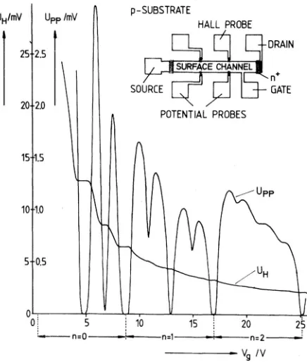
Figure 2.3 The first observation of the quantized Hall voltage. The voltage drop between
the potential probes Upp and the Hall voltage UH vs the gate voltage Vg at T = 1.5 K. The
constant magnetic field B is 18 Tesla and the source drain current, I, is 1 µA. The inset
illustrates a top view of the device. After von Klitzing et al. (1980).[5]
In the first observation of the IQHE [5], the experiment has been carried out by
mea-suring the longitudinal (Upp) and transverse (UH) voltages vs the gate voltage at a constant
magnetic field (Figure 2.3). A high magnetic field, 18 Tesla, was used in ref. [5], and the
Landau levels are well separated. The Fermi energy is a function of carrier concentration,
and by changing the gate voltage one can change the charge carrier concentration in the
system. Consequently, by changing the gate voltage one can move the Fermi energy relative
to the Landau levels.
A similar scenario can be achieved by varying the magnetic field (Figure 2.4). In the
absence of an external magnetic field, i.e., B = 0, the density of states have a constant value
as function of energy [Figure 2.4 (a)]. Let us consider a situation where there is an applied
EF
Density of States
Energy
B=0 Increasing B
(a) (b) (c) (d)
Figure 2.4 Landau level spectrum at different magnetic fields for a spin degenerate 2DES.
(a) At B = 0 there is no separation of Landau levels; therefore, the density of states have
a constant value vs the energy. (b) At a finite but small magnetic field, Landau levels are
formed but not yet fully separated. Fermi energy EF lies in the middle of a LL. (c) At this
magnetic field the Landau levels are completely separated and EF lies in between 2nd and
3rd Landau levels. In this situation the filling factor is equal 4, i.e., ν = 4. (d) Magnetic
field is at even higher value and EF lies within a LL.
considered to be delta functions with zero width, yet under real experimental conditions due
to scattering these delta function will be broadened; therefore, at smaller magnetic fields
even the Landau levels are formed will not be separated from each other [Figure 2.4 (b)],
i.e., the LL separation ~ωc has to be greater than the width of the LL. As the magnetic
field increases the separation between the Landau levels will increase; as a result, the overlap
between two Landau levels would become smaller and smaller. In addition, as the magnetic
field is swept the Landau levels move relative to the Fermi energy.
Let us consider a situation where the EF lies in between two Landau levels and all the
states below the Fermi level are occupied [Figure 2.4 (c)]. According to the Pauli exclusion
principle, electrons inside these states are not allowed to scatter to other states.
Conse-quently, all scattering events are suppressed and at this point the transport is dissipationless
and the resistance goes to zero.
Classically, in strong magnetic fields ωcτ 1,
σxx = e2n m∗ω2 cτ
σxy = e2n m∗ω
c
(2.33)
whereσxx andσxy are the diagonal and Hall conductivities, respectively [see eq. (2.31)]. Let
us assume that B =BN when EF lies between N and N + 1 Landau levels or between spin
up (↑) and spin down (↓) levels of the Nth LL. Then from eq. (2.19) and eq. (2.33) we get
σxy =
e2 h
νN. (2.34)
Remarkably during the same B-interval, where EF lies in between two Landau levels,
i.e., when the longitudinal resistance goes to zero (see Figure 2.3), Hall conductivity depends
only on e, h, and νN. Further it is quantized at integer multiples ofe2/h.
2.5.1 Shubnikov de Haas oscillations
-0.500 -0.25 0.00 0.25 0.50
4 8 12 16
T = 1.5 K
Rxx
(
)
B (T)
Figure 2.5 Shubnikov de Haas oscillations in a GaAs/AlGaAs Hall bar device at 1.5 K.
At high enough magnetic fields there exists energy gaps in the LL energy spectrum;
consequently, the density of states becomes a discrete function of 1/B, yet at lower magnetic
fields, where the Landau levels are not completely separated from each other [Figure 2.4
(b)], the density of states becomes a continuous periodic function of 1/B and it reflects in
longitudinal resistance as oscillations (Figure 2.5). These oscillations are called Shubnikov
de Haas (SdH) oscillations. Furthermore, these oscillations are periodic in inverse magnetic
part of the magnetoresistance ∆Rxx, i.e., only the SdH oscillations without the background,
can be expressed in the following form [12]
∆Rxx =R0
XT
sinh(XT)
exp(−π/ωcτ) cos
2πEF −EM
~ωc
−φ
(2.35)
where R0 is the zero field resistance, kB is the Boltzmann constant, EM is the energy of
the Mth sub-band. The factor XT/sinh(XT) is the temperature dependence of the SdH
oscillation amplitude and XT is given by [36]
XT =
2π2k BT
~ωc
. (2.36)
Experimentally ∆Rxx is often considered as a exponentially damped cosine function [39]
∆Rxx =Ae−α/Bcos(2πF/B) (2.37)
whereAis the amplitude of the oscillations,αis the damping factor, andF is the frequency.
The frequency F of the SdH oscillations is a measure of the carrier density.
2 3 4 5
8 12
16 20 24 28 32 36 40 44
Rxx
(
Ω
)
B-1 (T-1)
1/F
ν
Figure 2.6 Periodicity of SdH oscillations vs 1/B. Here F is the frequency of the SdH
oscillations, and the corresponding filling factor ν is shown in the top axis.
The densitynof the 2DES can be extracted from the frequencyF of the SdH oscillations.
In addition, the effective massm∗, the mass that the electron experience while moving relative
to the lattice in an applied electric or magnetic field, can be calculated from the temperature
the 1/B dependence of the SdH oscillation amplitude. Therefore, a study of SdH oscillations
at low temperature and low magnetic fields will be beneficial for measuring the parameters,
such as effective mass m∗, scattering time τ, and density n. As the oscillation amplitude
depends on the temperature we can use it to probe possibility of heating effects in a 2DES
due to radiation (see Chapter 4 for further details).
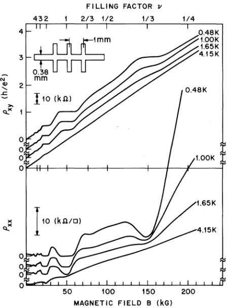
[image:35.612.193.417.255.559.2]2.6 Fractional quantum Hall effect
Figure 2.7 The first observation of the quantized Hall voltage at fractional filing factors
ν = 1/3. Magnetic field dependence ofρxy and ρxx is shown for a GaAs/Al0.3Ga0.7As sample
with n = 1.23×1011 cm2, µ = 90×103 cm/V s, using I = 1 µA. The Landau level filling
factor is defined by ν =nh/eB. After Tsui et al. (1982).[6]
As we already discussed in section 2.5, as the applied external magnetic field increases
the Landau levels go to higher and higher energies with respect to EF (Figure 2.4). Let us
at high enough magnetic fields and low temperatures. At higher magnetic fields l0 becomes
extremely small [eq. (2.12)]; consequently, it is important to consider the electron-electron
interactions to understand the behaviour of the carriers in such a system.[4]
Few years after the discovery of IQHE, the experimental work by D. C. Tsui and H. L.
St¨ormer led to the observation of a Hall plateau at a fractional filling factor ν = 1/3 (see
Figure 2.7) for the first time.[6] The fractional quantum Hall effect (FQHE) is characterized
by the observation of vanishing Rxx and quantization of Rxy at fractional filling factors (see
Figure 2.8). The FQHE state is an intrinsically many body, incompressible quantum liquid,
is often described by the Laughlin wavefunction.[4, 7]
Figure 2.8 Longitudinal resistance, Rxx, and the transverse resistance, Rxy, measured in a
GaAs/AlGaAs heterostructure device are plotted vs the magnetic field B. A series of Hall plateaus at fractional filling factors can be observed. After Mani et al. (1996).[10]
In a remarkable experimental observation, Mani et al. [10] describe a fractal nature of
FQHE. According to the authors, it is possible to reconstruct the main sequence of FQHE
for ν < 1 using IQHE where filling factor ν > 1. Furthermore, this reconstruction of the
fractional quantum Hall states suggests a possibility of finding the missing fractions in the
CHAPTER 3
ELECTRICAL TRANSPORT IN 2DES UNDER MW IRRADIATION
In Chapter 2 we already discussed the interesting physical phenomenon that have been
observed in 2DES, and most interestingly the vanishing resistance under IQHE[5], section 2.5,
and FQHE[6, 7], section 2.6, conditions. In 2002 Mani et al. reported their experimental
results[11] on discovering a zero resistance state in a 2DES under microwave irradiation at
low temperatures. Major part of the thesis is based on these MW induced magnetoresistane
oscillations (MIMO) observed in 2DES; therefore, this chapter will give a brief introduction
to the to the MW induced ZRS and to MIMO.
3.1 Microwave induced zero resistance states
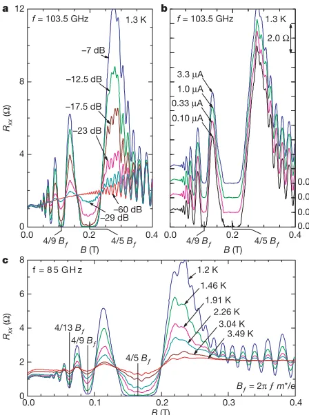
Figure 3.1 illustratesRxxvsBresponse upto 10 Tesla for a high mobility 2DES specimen
under microwave irradiation at f = 103.5 GHz. It can be easily seen the existence of Hall
plateaus and zero resistance at higher magnetic fields, and also there is an extra set of
resistance oscillations appear at the low magnetic fields under MW irradiation, see Figure 3.1
inset. A closer look at the behaviour of Rxx at low magnetic fields under MW irradiation
reveals that the minima of these oscillations actually reach zero (Figure 3.2).
The behaviour of Rxx with and without MW radiation as a function of B is shown in
Figure 3.2 for f = 103.5 GHz at low magnetic fields. It is clear that the trace without MW
radiation does not show any oscillations at low magnetic fields, yet with MW irradiation the
Rxx vsB shows a set of oscillations in which at certain magnetic fields theRxx goes to zero,
i.e., Rxx →0. It is found that these characteristic magnetic fields can be expressed as [11]
B =
4 4j+ 1
Figure 3.1 The first observation of radiation induced zero resistances on high-mobility
GaAs/AlGaAs heterostructure devices at 103.5 GHz. Quantum Hall effects occur at high B
asRxx →0. Inset shows an expanded view of the low-B data where Rxx →0 in the vicinity
of 0.198 Tesla under microwave excitation. After Mani et al. (2002).[11]
where j = 1,2, . . ., and
Bf =
2πf m∗
e . (3.2)
Further a close inspection of the Hall effect in the vicinity of these MW induced ZRS, unlike
IQHE and FQHE, is not accompanied by a Hall plateau.[11]
3.2 Microwave induced magnetoresistance oscillations
After the initial discovery of MW induced ZRS, there have been an increasing interest
in the field of radiation induced magneto-transport and a lot of research has been done both
experimentally [11, 16, 20–24, 27, 28, 32, 35, 37–39, 64–70] and theoretically [40, 41, 43, 47, 48,
50, 51, 55, 59, 62, 72, 73, 75–80] in order to understand the physics of MIMO. This section will
review the experimental work has been done in this field and the next section, section 3.3,
will discuss the theoretical developments on understanding the physics of MW induced ZRS
and MIMO in 2DES.
It is already mentioned that the magnetic fields at which the ZRS appear scale with
the MW frequency f, effective mass m∗ and the electronic charge e[eq. (3.1) and eq. (3.2)].
Figure 3.2 Rxx andRxy vsB with and without microwave radiation at 103.5 GHz. Unlike in
the QHE, there are no Hall plateaus observed when theRxx →0 under microwave excitation.
After Mani et al. (2002).[11]
can be observed only upto about 0.25 Tesla and does not overlap with SdH oscillations
[see Figure 3.3 (a)]. On the other hand at higher frequencies MIMO extends to higher
magnetic fields as expected; consequently, it overlaps with SdH oscillations [see Figure 3.3
(b)].[11, 22, 29, 31]
Microwave power, DC current, and temperature dependence of MIMO are shown in
Fig-ure 3.4 (a), (b), and (c), respectively. The amplitude of the MW induced magnetoresistance
oscillations appear to be increasing with the MW power and ultimately the resistance
min-ima reach zero [see Figure 3.4 (a)]. Later it has found that MIMO amplitude is proportional
to the square root (non-linear) of the MW power P, i.e., MIMO amplitude ∝ √P.[13, 37]
Furthermore, there are other reports indicating that MIMO amplitude is linear in MW
power.[16, 50] According to the ref. [11] MIMO are not sensitive to the DC current passing
through the specimen [see Figure 3.4 (b)]. Temperature dependence of MW induced ZRS
as well as MIMO have been studied, and Figure 3.4 (c) illustrates that the temperature
dependence of a ZRS near 4/5Bf and MIMO at lower magnetic fields.[11] It can clearly be
seen that as the temperatures increases MIMO amplitude become smaller and smaller.
Rather interesting phenomenon have been observed at higher frequencies as the MIMO
ef-Figure 3.3 Development of microwave induced zero resistance state for different frequencies. After Mani et al. (2002). [11]
fects.[36] Under quantum Hall effects conditions a plateau in the Hall effect have been
ob-served as the resistance reach zero (see section 2.5, and section 2.6). As the MW induced
ZRS at higher frequencies overlap with quantum Hall plateaus at higher filling factors, it has
been reported that the Hall plateau disappear as MIMO reach zero resistance.[36] In other
words, photoexcitation replace the IQHE with ordinary (classical) Hall effect. The reason
for this kind of behaviour is yet to be understood.
3.3 Physical origin of microwave induced magnetoresistance oscillations
Microwave induced zero-resistance states appear when the associatedB−1-periodic
mag-netoresistance oscillations grow in amplitude and become comparable to the dark resistance
[image:40.612.192.416.72.393.2]Figure 3.4 (a) Microwave power, (b) DC current, and (c) temperautre dependence of MIMO. After Mani et al. (2002). [11]
thereof,[64, 65] are now understood via the the displacement model,[40, 43, 72, 77] the
non-parabolicity model,[73] the inelastic model,[50, 75] and the radiation driven electron orbit
model.[47, 48, 51, 76] In theory, some of these mechanisms can drive the
magnetoconductiv-ity to negative values at the oscillatory minima. Negative conductivmagnetoconductiv-ity then triggers an
instability in favor of current domain formation, and zero-resistance states.[41, 59] Following
sections will provide a brief overview for some of these models.
3.3.1 Displacement model
Several theoretical approaches have been reported[40, 43, 72, 77] in order to describe the
behaviour of MIMO in 2DES that are based on displacement model. Here, this section will
briefly describe the theory by Durst et al.[40] in order to illustrate the basic idea of the
[image:41.612.193.417.70.371.2]is to make Nr; NeEdcx. Jx vanishes to
zeroth order inEdcby symmetry, and for linear response,
we expand to first order inEdc, and divide byEdc to find
the longitudinal conductivity, xx. We find that the
radiation-induced change in the longitudinal conduc-tivity is proportional to an integral of the partial
deriva-tive @Nr; !Nr0; =@xR. The density of
states can be roughly modeled by N N0
N1cos2=!c. The final integral over can now be
done and, at least for!=!c large compared toN0=N1,
the result is
xx / sin2!=!c; (2)
with a positive coefficient. This form, which resembles
the derivative of the density of states @N=@j!,
arises because the main contribution is from initial states near the center of filled broadened Landau levels, which are scattered to empty broadened levels, and the available
phase space is enhanced or diminished forxpositive or
negative, depending on the energy change! modulo !c
(see Fig. 1). It is clear from experiment thatxy is nearly
100 times larger thanxxand is not significantly affected
by the radiation. Therefore, inverting the conductivity
tensor yields xx2xyxx, which has the period and
phase of the oscillations observed in experiment.
While the above treatment is highly oversimplified, it indicates that disorder plays a crucial role and may be all that is necessary to obtain the radiation-induced oscilla-tions. This suggests that a diagrammatic (Kubo formula) calculation of the conductivity, including radiation and disorder but neglecting electron-electron interactions,
will be sufficient to reproduce the effect. This calculation is presented below.
In the Landau gauge and the rotating-wave approxima-tion (we neglect both counter-rotating and guiding-center terms in the coupling to radiation), the Hamiltonian is
H X
k;n
n!ccynkcnk X
k;n;k0;n0
cynkcn0k0Vn;k;n0;k0
eE‘ 2 p X k;n n p
cynkcn1;kei!tcyn1;kcnkei!t; (3)
wherenis the Landau level index,kis theycomponent of
momentum, cnk is the electron annihilation operator,
Vn;k;n0;k0 are the matrix elements of the disorder potential
Vimpr, and E is the magnitude of the electric field
component of the microwave radiation. Following the calculation of Ando [5] for the zero-radiation case, we shall include disorder within the self-consistent Born
approximation (SCBA) and assume VimprVimpr0
2#=mrr0, where#1=2$is the elastic
scatter-ing rate in zero magnetic field. This assumption of
-correlated disorder, while somewhat inappropriate for
the long-ranged impurity potentials associated with modulation doping, significantly simplifies the problem by eliminating the momentum dependence of the self-energy. Yet, as we shall see, it manages to capture the important physics rather well. To all orders in the disorder and radiation, the Green’s functions are given by the diagrams in Fig. 2(a). Since the radiation terms connect neighboring Landau levels, evaluating these diagrams for
the retarded or advanced Green’s functions, GR;Anmt1; t2,
yields a matrix equation in Landau level indicesnandm.
(The Green’s functions are proportional to an identity
matrix in the momentum label k, which is therefore
dropped.) The presence of radiation renders this an inherently nonequilibrium problem which requires the approach of Kadanoff and Baym and Keldysh (see
(a)
+
+
=
+
(b) (d) (c) dc dc dc dc dc dc dc dc dc dcFIG. 2. Diagrams for (a) Green’s function and (b) polariza-tion bubble including radiapolariza-tion and disorder within SCBA. Disorder lines are dotted. Photon lines are curvy. The vertex of the polarization bubble is dressed with ladders of disorder lines. When the no-photons-crossed-by-disorder-lines conserv-ing approximation is made, diagrams like those in (c) are included while those in (d) are neglected.
ω
cV
ω
ε
n = nω
c + eEdcxn+2
n+1
n+3
n
+∆x
−∆x
FIG. 1. Simple picture of radiation-induced disorder-assisted current. Landau levels are tilted by the applied dc bias. Electrons absorb photons and are excited by energy !. Photoexcited electrons are scattered by disorder and kicked to the right or to the left by a distancex. If the final density of states to the left exceeds that to the right, dc current is enhanced. If vice versa, dc current is diminished. Note that electrons initially near the center of a Landau level (where the initial density of states is greatest) will tend to flow uphill for
!=!c integer1=4.
086803-2 086803-2
Figure 3.5 Simple illustration of radiation induced disorder assisted current is shown.
Adopted from ref. [40].
photon and excited by an energy ~ω.
ω = 2πf (3.3)
where f is the MW frequency. In the presence of disorder these excited electrons can be
scattered and hence the conductivity will be modified. Application of a DC bias will result
in a finite tilt in the Landau levels (see Figure 3.5). Photoexcited electrons can move to
the left (positive bias) or right (negative bias) by a distance of ∆x after scattering by a
disorder depending on ω and ωc. If the density of states to the left is greater than that of
to the right then the DC current will enhanced and if the density of states to the left is less
than that of to the right then the DC current will reduced. Consequently, oscillations in the
conductivity can be manifested in the photoexcited specimen.[40] According to this theory,
the observed radiation induced magnetoresistance oscillation can be explained considering
only the disorder assisted scattering in the presence of MW radiation. According to the
authors, numerical simulations using the theoretical model are in good agreement with the
experimental observations reported in ref. [11] regarding the phase and the period of the
experiments[11] is not universal and it can vary from 0 to 1/2 depending on the disorder and
the intensity, yet the nodes observed at integer values of ω/ωc appeared to be insensitive
to these parameters. According to the displacement model the photon assisted acoustic
phonon scattering is responsible for the experimentally observed temperature dependence of
the radiation induced magnetoresistance oscillations amplitude.[72]
3.3.2 Inelastic model
Within this theory the magnetoresistance oscillations induced by the microwave
diation is governed by a change in the electron distribution function induced by MW
ra-diation.[50, 75] Since the density of states relate to the Landau quantization and it is an
oscillatory function of B−1, the correction to the electron distribution function includes a
oscillatory structure as well. As a result, this will generate a contribution to the DC
conduc-tivity that oscillates with ω/ωc. Here the dominant contribution to the effect comes from
inelastic scattering, mainly electron-electron scattering, and therefore the effect is strongly
temperature dependent. Furthermore, the magnitude of the effect increases with the
decreas-ing temperature as T−2 for k
BT ~ω and as T−1 for kBT ~ω.[50, 75] Also according to
the theory, the MW induced effect is linear in MW power for not too strong power levels.
Although the theory has been developed considering only the linearly polarized MW
radia-tion, the results are predicted to be the same for circularly polarizaed radiation away from
ω =ωc. In addition, it also predicts insensitivity to the orientation of the MW field, yet the
recent experimental results suggests otherwise [70, 71]; see Chapter 5 for more details about
the experimental results on polarization dependence of MIMO.
3.3.3 Radiation driven electron orbit model
The radiation driven electron orbit model [47, 48, 51, 76] is based on a perturbation
treatment for elastic scattering due to charged impurities to an exact solution for the
har-monic oscillator wave function under MW radiation. In the absence of MW radiation, the
charged impurities. In the theoretical model, the authors consider a 2DES subjected to a
magnetic field applied along the z-axis and a DC electric field along the x direction, which
is responsible for the transport through the 2DES. In addition, the system is subjected to a
AC electric field EM W due to linearly polarized MW radiation. The linearly polarized MW
radiation is characterized by the polarization angle α,
tanα = Ey
Ex
(3.4)
whereExandEyare the respective amplitudes of the MW fieldEM W alongxandydirections.
In such a situation the average distance advanced by the electron ∆XM W in each scattering
event can be written as,
∆XM W = ∆X0+Acos(ωτ) (3.5)
where ∆X0 is the average distance advanced by an electron in the absence of MW radiation
and Acos(ωτ) is the distance advanced due to MW radiation. Here ω and τ are the MW
frequency and impurity scattering time, respectively.[76] The amplitude A of the average
distance advanced due to MW radiation is given by [76]
A= eE0
m∗q ω2(ω2
c−ω2)
2 ω2cos2α+ω2
csin2α +γ
4
. (3.6)
Here E0 is the MW field intensity and γ is a sample dependent parameter, which has a
significant effect on the motion of MW driven electron orbits and hence the MW induced
effects. According to eq. (3.6), for γ > ω the value of γ dominates over the other terms and
the value of A become independent of α, i.e., forγ > ω the MW induced effect is
indepen-dent of the direction of the linearly polarized MW radiation. On the other hand, if γ < ω
the polarization angle α dependent term dominates, and hence the effect become
polariza-tion dependent. Polarizapolariza-tion direcpolariza-tion dependence of MW induced resistance oscillapolariza-tions is
discussed in great detail in Chapter 5.
to the theory, increasing temperature will damp ∆XM W, and thereby reducing the oscillation
amplitude. Further, the authors propose that electron acoustic-phonon interactions as a
possible explanation for the temperature dependence of the MW induced effect.[47, 48]
3.3.4 Non-parabolicity model
The non-parabolicity model considers a classical model for transport in a 2DES
un-der applied a magnetic field normal to the 2D plane and unun-der strong irradiation.[73] Near
cyclotron resonance, i.e., ω = ωc, in the presence of linearly polarized MW radiation, the
electron spectrum demonstrates a weak non-parabolicity, and this will cause a small change
in the electron effective mass. Consequently, this gives rise to a change in the diagonal
con-ductivity, but not in the transverse voltage, giving rise to MIMO. Further, in this theory, the
MIMO only occurs for linearly polarized MW radiation, and not for circularly polarized MW
radiation. The effect of MW radiation on the diagonal conductivity depends on the
orienta-tion between the DC electric field and MW electric field; consequently, the non-parabolicity
model also predicts a polarization dependence for MIMO.[73] Even though the model can
predict the MW induced oscillations in the diagonal conductivity near cyclotron resonance,
experimentally observed oscillations in the vicinity of the harmonics of the cyclotron
reso-nance cannot be modeled [11] in the context of the model given in ref. [73].
Thus far we discussed the experimental and theoretical work done in the past to
investi-gate the properties of the MIMO observed in high quality 2DES. It is clear that the existing
theoretical models differ in their opinion about the dependence of MIMO on physical
param-eters, such as temperature, polarization, power, etc. In the following chapters, Chapter 4,
and Chapter 5, we will present the experimental work that has been done towards
under-standing the physics of MIMO in terms of heating due to MW radiation and polarization
CHAPTER 4
MICROWAVE INDUCED ELECTRON HEATING
4.1 Introduction
In chapter 3, section 3.1 and section 3.2 already discussed the experimental and
theo-retical work that has been done towards understanding the physics of MIMO. As has been
shown in the experiments, the energy absorption rate is small in high-mobility electron
sys-tems at low temperatures. However, this does not imply a negligible electron heating, since
the electron energy-dissipation rate is also small because of weak electron-phonon scattering
at low temperatures. Indeed, theory has [45, 49, 51], in consistency with common
experi-ence, indicated the possibility of microwave induced electron heating in the high mobility
2DES in the regime of the radiation induced magnetoresistance oscillations. Not
surpris-ingly, under steady state microwave excitation, the 2DES can be expected to absorb energy
from the radiation field. At the same time, electron-phonon scattering can serve to dissipate
this surplus energy onto the host lattice [49]. Lei et al. [49] have determined the electron
temperature, Te, by balancing the energy dissipation to the lattice and the energy
absorp-tion from the radiaabsorp-tion field, while including both intra-Landau level and inter-Landau level
processes. In particular, they showed that the electron temperature, Te, the longitudinal
magnetoresistance, Rxx, and the energy absorption rate, Sp, can exhibit remarkable
corre-lated non-monotonic variation vsωc/ω, whereωc is the cyclotron frequency [eq. (2.14)], and
ωis the radiation frequency [eq. (3.3)].[49] Under these circumstances, it would be interesting
to investigate experimentally the possibility of electron heating due to microwave radiation
in a regime where microwave induced magnetoresistance oscillations are observable. In such
a situation, some questions of experimental interest are: (a) How to probe and measure
elec-tron heating in the microwave-excited 2DES? (b) What is the magnitude of elecelec-tron heating
characteristic in microwave radiation induced transport?
4.2 Effect of MW radiation on SdH oscillation amplitude
The SdH oscillation amplitude shows strong sensitivity to the electron-temperature.[49]
Consequently, an approach to the characterization of electron-temperature or possibility of
heating due to MW radiation could involve a study of the amplitude of the SdH
oscilla-tions, which also occur in Rxx in the photo-excited specimen. Typically, SdH oscillations
are manifested at higher magnetic fields, B, than the radiation induced magnetoresistance
oscillations, i.e., B > Bf = 2πf m∗/e, eq. (3.2), especially at low microwave frequencies, say
f ≤50 GHz at T ≥1.3 K. On the other hand, at higher f, SdH oscillations can extend into
the radiation induced magnetoresistance oscillations. In a previous study, Mani et al. [31]
has reported that the SdH oscillation amplitude scales linearly with the average background
resistance in the vicinity of the radiation induced resistance minima, indicating the SdH
oscillations vanish in proportion to the background resistance at the centers of the radiation
induced zero-resistance states. In ref. [29], the authors discuss damping of SdH oscillations
and a strong suppression of magnetoresistance in a regime where microwaves induce
intra-Landau-level transitions. Kovalev et al. [22] have reported the observation of a node in the
SdH oscillations at relatively high-f. Both ref. [31] and ref. [22] examined the range of
ωc/ω ≤1, whereas ref. [29] examined the ωc/ω ≥1 regime.
Lei et al. have suggested, in a theoretical study, that a modulation of SdH oscillation
amplitude in Rxx when the 2DES is subjected to irradiation results from electron heating
caused by the radiation in a region where there is no overlapping of SdH oscillations and
MIMO.[49] Furthermore, they have shown that, inωc/ω ≤1 regime, bothTe andSp exhibit
similar oscillatory features, while in ωc/ω ≥ 1 regime, both Te and Sp exhibit a relatively
flat response.
Here, we investigate the effect of microwaves on the SdH oscillation amplitude over
2Bf ≤ B ≤ 3.5Bf, i.e., 2ω ≤ ωc ≤ 3.5ω. In particular, we compare the relative change
radiation), with the changes in the SdH amplitude under microwave excitation at different
microwave power levels and frequencies (at a constant temperature). The change in the
electron temperature ∆Te due to MW radiation can be extracted. In good agreement with
theory, the results indicate ∆Te≤50 mK over the examined regime.
0.0000 0.125 0.250 0.375
4 8 12
16 Bf 2Bf 3Bf
3.2 mW
1.6 mW
1 mW
0.6 mW
0.3 mW Rxx
(
)
B (T) Dark
44 GHz B
f=2 fm*/e
Fit range
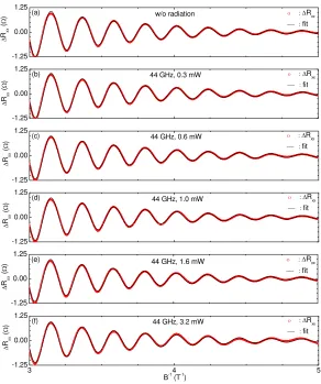
Figure 4.1 Microwave induced magnetoresistance oscillations and SdH oscillations inRxx are
shown at 1.5 K for 44 GHz at different power levels P. A horizontal marker (green) shows
the field range (2Bf ≤B ≤7/2Bf) where SdH fits were carried out.
The lock-in based electrical measurements, Appendix B, were performed on Hall bar
devices fabricated from high quality GaAs/AlGaAs heterostructures. Experiments were
carried out with the specimen mounted inside a waveguide and immersed in pumped liquid
helium, see Appendix B for further details. The frequency spanned 25 ≤ f ≤ 50 GHz at
source power levelsP ≤5 mW. Magnetic-field-sweeps ofRxx vs P were carried out at 1.6 K
at 41.5 GHz, and at 1.5 K at 44 GHz and 50 GHz.
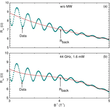
Microwave induced magnetoresistance oscillations can be seen in Figure 4.1 atB ≤0.175
Tesla, as strong SdH oscillations are also observable under both the dark and irradiated
conditions forB ≥0.2 Tesla. Over the interval 2Bf ≤B ≤3.5Bf, where the SdH oscillations
are observable, one could observe small variations in the background Rxx at higher power
6 7 8 9 10 (a) Rback w/o MW Rx x ( : ) Data 5 back 7 8 9 10
44 GHz, 1.6 mW
Rx x ( : ) (b)
3 4 5
[image:49.612.196.418.72.289.2]5 6 Rback B-1 (T-1 ) Data
Figure 4.2 Small variations in the SdH oscillations background (a) w/o and (b) w/ MW
ra-diation are shown. Rback is a NLSF to a order 5 polynomial, which represent the backbround
variations in SdH oscillations.
Rback, was subtracted from the magnetoresistance data,
∆Rxx =Rxx−Rback. (4.1)
Figure 4.3 (a)-(f) shows the background subtracted Rxx, i.e., ∆Rxx, measured without
[Fig-ure 4.3 (a)] and with [Fig[Fig-ure 4.3 (b)-(f)] microwave radiation versus the inverse magnetic field
B−1. To extract the amplitude of the SdH oscillations, we performed a standard Nonlinear
Least Squares Fit (NLSF) on ∆Rxx data with an exponentially damped sinusoid,
∆Rxx =−Ae−
α B cos 2πF B (4.2)
Here, A is the amplitude, F is the SdH frequency, B is the magnetic field, and α is the
damping factor. The fit results for the dark-specimen ∆Rxx data are shown in the Figure 4.3
(a) as a solid line. This panel suggests good agreement between data and fit in the dark
-1.25 0.00 1.25
(a) w/o radiation 2'Rxx
fit ' Rx x ( : ) 0.00 1.25
(b) 44 GHz, 0.3 mW 2'Rxx
fit Rx x ( : ) -1.25 ' R -1.25 0.00 1.25
(c) 44 GHz, 0.6 mW 2'Rxx
fit ' Rx x ( : ) 0.00 1.25
(d) 44 GHz, 1.0 mW 2'Rxx
fit Rx x ( : ) -1.25 ' -1.25 0.00 1.25
(e) 44 GHz, 1.6 mW
'
Rx
x
(
:
) 2'Rxx
fit
0.00 1.25
(f) 44 GHz, 3.2 mW 2'Rxx
fit ' Rx x ( : )
3 4 5
-1.25
B-1 (T-1)
'
Figure 4.3 (a) The background subtractedRxx, i.e., ∆Rxx, in the absence of radiation (open
circles) and a numerical fit (solid line) to eq. (4.2) are shown here. Panels (b)-(f) show the
∆Rxx and the fit at the indicated P.
power spanning approximately 0 ≤ P ≤ 3 mW, see Figure 4.3 (b)-(f). The parameters α
and F are insensitive to the incident radiation at a constant temperature, consequently, we
can fix α and F to the dark-specimen constant values. In Figure 4.3, panels (b)-(f) show
the T = 1.5 K ∆Rxx data (open circles) and fit (solid line) obtained with f = 44 GHz for
different MW power levels. The SdH oscillations amplitudeAextracted from the NLSFs are
exhibited vs the microwave power in Figure 4.4. Here,Adecreases with increasing microwave
[image:50.612.159.451.73.422.2]90 100
(
:
)
44 GHz
0.0 0.5 1.0 1.5 2.0 2.5 3.0 3.5 80
A
(
P (mW)
Figure 4.4 MW power dependence of the SdH amplitude A at 44 GHz.
4.3 Temperature dependence of SdH oscillation amplitude
Next, we examine the influence of temperature on the SdH oscillation amplitude.
Fig-ure 4.5 shows Rxx vs B with the temperature as a parameter. It is clear [see the dashed
(black) lines in Figure 4.5] that increasing the temperature rapidly damps the SdH
oscilla-tions at these low magnetic fields. In order to extract the SdH oscillation amplitude from
these data, we used the same fitting model, see eq. (4.2), as described previously. But, for
the T-dependence analysis, α was separated into two parts,αT0 and β∆T,
α=αT0 +β∆T (4.3)
since we plan to relate the change in the SdH oscillation amplitude for a temperature
incre-ment to the observed change in the SdH amplitude for an increincre-ment in the microwave power
at a fixed f. Here αT0 represents the damping at the base temperature, T0, and β∆T is the
additional damping due to the temperature increment,

![Figure 2.2 Energy band diagram of a modulation doped heterojunction.[1]](https://thumb-us.123doks.com/thumbv2/123dok_us/9220212.990040/24.612.233.363.71.217/figure-energy-band-diagram-modulation-doped-heterojunction.webp)