HONEYWELL
_
DPS/LEVEL
68 &
DPS8M
MULTICS
MULTICS PROCESSOR MANUAL
SUBJECT
Description of the Multics Processor
SPECIAL INSTRUCTIONS
This manual supersedes AL39-00, dated April 1976 and Addendum A, AL39-00A, dated September 1976. The manual has been extensively revised. Change bars in the margin indicate technical additions and changes; asterisks denote deletions.
ORDER NUMBER
AL39-01 April 1979
*
PREFACE
This manual describes the processors used in the Multics system. These are
the DPS/L68, which refers to the DPS, L68 or older model processors (excluding
the GE-645) and DPS 8M, which refers to the DPS 8 family of Multics processors,
i.e. DPS 8/70M, DPS 8/52M and DPS 8/52M. The reader should be familiar with
the overall modular organization of the Multics system and with the philosophy
of asynchronous operation. In addition, this manual presents a discussion of
virtual memory addressing concepts including segmentation and paging.
The manual is intended for use by systems programmers responsible for
writing software to interface with the virtual memory hardware and with the
fault and interrupt portions of the hardware. It should also prove valuable to
programmers who must use machine instructions (particularly language translator implementors) and to those persons responsible for analyzing crash conditions in system dumps.
This manual includes the processor capabilities, modes of operation,
functions, and detailed descriptions of machine instructions. Data
representation, program-addressable registers, addressing by means of
segmentation and paging, faults and interrupts, hardware ring implementation,
and cache operation are also covered.
Section 1
Section 2
Section 3
11/85
CONTENTS
Introduction . . . .
Multics Processor Features . . . • . • Segmentation and Paging • . . . . Address Modification and Address
Appending . . . .
Faults and Interrupts . . .
Processor Modes of Operation . . . . .
In struc tion Ex ecution Modes . . . . .
Normal Mode
P r i v i 1 e g ed t40 d e . . . . Addressing Modes
Absolute Mode Append Mode Bar Mode . . .
Processor Unit Functions.
Appending Unit . . . .
Associative Memory Assembly Control Un it
Operation Unit Decimal Un i t
Data Representation • . • • . Information Organization Position Numbering .
Number System . . . . •
Information Formats Data Parity . . . . Representation of Data .
Numeric Data . . . •
Fixed-point Binary Data
Fixed-Point Binary Integers . Fixed-point Binary Fractions Floating-point Binary Data
Overlength Registers Normal ized Numbers Decimal Data . . • . . .
Decimal Data Values . Alphanumeric Data . . • . .
Character String Data • • • •
Bit String Data Program Accessible Registers
Accumulator Register (A) •
Quotient Register (Q) . • . . .
Accumulator-Quotient Register (AQ) •
Exponent Register (E) • • • • • • • • • • •
Exponent-Accumulator-Quotient Register (EAQ) Index Registers (Xn) . • • . .
Indicator Register-(IR) Base Address Register (BAR)
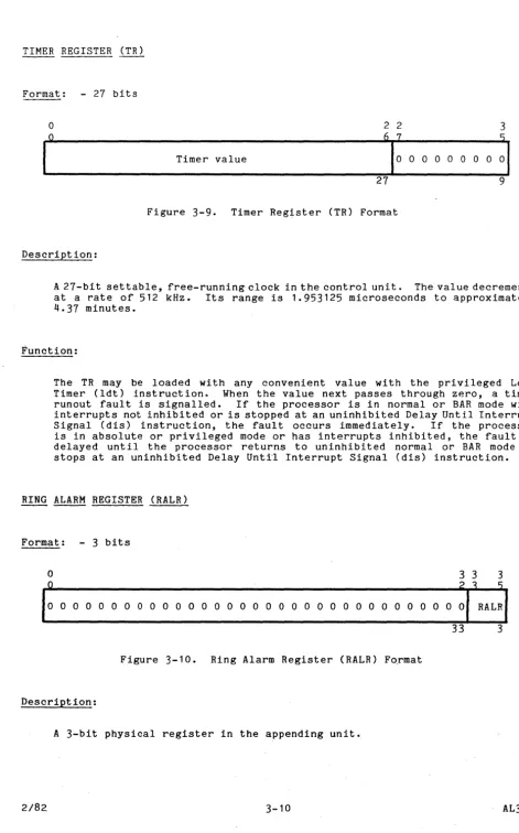
Timer Register (rR) . • • . .
Ring Alarm Register (RALR) Pointer Registers (PRn)
Address Registers (ARn) • . • •
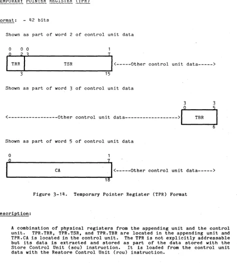
Procedure Pointer RegIster (PPR) Temporary Pointer Register (TPR)
Section 4
C'JNTENTS (cont)
Page
Descriptor Segment Base Register (DSBR) 3-16
Segment Descriptor Word Associative Memory
(SDWAM) - DPS/L68 and DPS 8M . . . . . 3-18
Page Table Word Associative Memory (PTWAM)
-DPS/L68 and DPS 8M . . . 3-20
Fault Register (FR) - DPS/L68 . 3-23
Fault Register (FR) - DPS 8M . . 3-25
Mode Register (MR) - DPS and L68 • 3-27
Mode Reg ister (MR) - DPS 8~ . . . . 3-30
Cache Mode Register (CMR) - DPS and L68 3-32
Cache Mode Register (CMR) - DPS 8M . . . 3-34
Control Unit (CU) History Registers - DPS
and L68 . . • . . 0 . 0 0 . • 0 . . . 0 . 0 3-37
Control Unit (CU) History Registers - DPS 8M 3-39
Operations Unit (OU) History Registers 0 0 0 3-41 Decimal Unit (DU) History Registers - DPS
and L68 0 0 • 0 . 0 0 . 0 0 0 0 0 0 0 0 3-43
Decimal/Operations Unit (DU/OU) History
Registers - DPS 8M 0 0 . 0 . • 0 . . . 3-46
Appending Unit (APU) History Registers - DPS
and L 6 8 0 . • 0 0 0 • 0 0 0 0 • 0 0 . 0 3 -4 9
Appending Unit (APU) History Registers - DPS
8M 0 0 0 . • • 0 0 • 0 0 0 0 • 0 0 . 0 3-51
Configuration Switch Data - DPS and L68 3-54
Configuration Switch Data - DPS 8M 0 3-56
Control Uni t Data 0 0 0 0 3-58
Decimal Unit Data 3-63
Machine Instructions
Instruction Repertoire 0
Arrangement of Instructions 0
Basic Operations 0 0 0 0 0 0 0 0 0 0 0 0
Extended Instruction Set (eis) Operations EIS Single-~ord Operations . .
EIS Multiword Operations. 0 0 Format of Instruction Description Definitions of Notation and Symbols
Main Memory Addresses 0 0 0 0 . . . 0 • •
Index Values 0 0 0 0 0 0 0 • 0 0
Abbreviations and Symbols 0 0 0 . 0 0 • 0 Register Po si tions and Conten ts 0 . 0 • 0 Other Symbols 0 0 0 0 0 0 0 • 0 0 . 0 • 0 Common Attributes of Instructions
Illegal Modification 0 0 0 0
Parity Indicator 0 0 0 0 0 0 0 0
Instruction Word Formats • 0 0 0 0 0 0 0 • 0 Basic and EIS Single-Word Instructions
Indirect Words 0 • 0 0 0 0 •
EIS Multiword Instructions 0 0 . 0 0
EIS Modification Fields (MF) 0 0 0 0 • 0
MF Coding Examples 0 0 0 • 0 0 0 0 EIS Operand Descriptors and Indirect
Pointers • • 0 00 0 0 0 • • 0 0 . 0 Operand Descriptor Indirect Pointer
Fo rmat • 0 0 • • 0 0 0 • 0 0 0 0 • 0
Alphanumeric Operand Descriptor Format Numeric Operand Descriptor Format Bit-string Operand Descriptor Format 0 Fixed-point Arithmetic Instructions
Fixed-Point Data Movement Load 0 0 0 • 0
Fixed-Point Data Movement Store 0 Fixed-Point Data Movement Shift 0 Fixed-Point Addition
Fixed-Point Subtraction 0 0 0 0 0 • 0 • 0 4-1 4-1 4-1 4-1 4-1 4-2 4-2 4-2 4-4 4-4 4-4 4-4 4-5 4-5 4-6 4-6 4-6 4-6 4-6 4-7 4-8 4-9 4-11 4-11
4-110 1
11/85
CONTENTS (cont)
Fixed-Point Multiplication Fixed-Point Division
Fixed-Point Negate • . . • .
Fixed-Point Comparison Fixed-Point Miscellaneous . Boolean Operation Instructions .
Bodlean AND . . . . • • . . • . • .
Boolean Or . . • • • .
Boolean Exclusive Or Boolean Comparative And •
Boolean Comparati I/e Not . • • • . Floating-Point Arithmetic Instructions.
Floating-Point Data Movement Load . Floating-Point Data Movement Store Floating-Point Addition . • . . Floating-Point Subtraction
Floating-Point Multiplication . . • .
Floating-Point Division . . . .
Floating-Point Negate . . . • .
Floating-Point Normalize Floating-Point Round Floating-Point Compare
Floating-Point Miscellaneous
Transfer Instructions • . . . . . . . .
Pointer Register Instructions . . • .
Pointer Register Data Movement Load . Pointer Register Data Movement Store Pointer Register Address Arithmetic Pointer Register Miscellaneous Miscellaneous Instructions .
Calendar Clock . . • • .
Derail . • . . •
Execute . . . . • Master Mode Entry •• No Operation
Repeat . . • • •
Ring Alarm Register •
Store Base Address Register • .
Translation • . • • . . • • • . . . • . .
Register Load . • • • • • . • . . • • .
Privileged Instructions
Privileged - Register Load Privileged - Register Store
Privileged - Clear Associative Memory • . Privileged - Configuration and Status • . Privileged - System Control • .
Privileged - Miscellaneous Extended Instruction Set (EIS) • •
EIS - Address Register Load
EIS - Address Register Store • . • .
EIS - Address Register Special Arithmetic EIS - Alphanumeric Compare
EIS - Al phanumeric Move • . EIS - Numeric Compare . • •
EIS - Numeric Move • • • . . . • .
EIS - Bit String Combine . • • • .
EIS - Bit String Compare
EIS - Bit String Set Indicators. EIS - Data Conversion . • . . •
EIS - Decimal Add i tion • . . •
EIS - Decimal Subtraction . • •
EIS - Decimal Multiplication • . • • . •
EIS - Decimal Division • . • .
Micro Operations For Edit Instructions .
Section 5
Section 6
Section 1
CONTENTS (cont)
Micro Operation Sequence Edit Insertion Table
Edit Flags • • • • • • •
Terminating Micro Operations
MVNE and MVE Diff~rences • •
Numeric Edit • • • • • • • • . • • • •
Alphanumeric Edit • • • •
Micro Operations • • • • • • . • • •
Micro Operation Code Assignment Map
Addressing -- Segmentation And Paging • • . • • Address ing Modes • • • • •
Absolute Mode •
~Append Mode • Segmentation • • •
Paging • • • • • • • • • • • • • • • • • • • Changing Addressing Modes
Address Appending • • • •
Address Appending Sequences • • • • • • . Append ing Un i t Data Word Formats.
Page Table Word (ptw) Format
Virtual Address Formation • . . • . . • • • Definition of Virtual Address
Types of Virtual Address Formation
Symbology (aIm) • • • . •
Symbolic Fields • • • • • . • . AIm Pseudo-Instructions • • • • • • Computed Address Formation • • • •
The Address Modifier (TAG) Field . • • •
General Types of Computed Address Modification • • • • • • • • . • • Computed Address Formation Flowcharts Register (r) Modification . . . . • • Examples: . • • • • • • . • • • • • • Register Then Indirect (ri) Modifications
Examples: • • • • . . • • • • • • . Indirect Then Register (ir) Modification
Examples: • • • • • • • • • • • Indirect Then Tally (it) Modification Special Address Modifiers • • • . • • • .
Indirect to Pointer (ITP) Modification • • • • • • • • Indirect to Segment (ITS)
Modification • • . . • • • • Effective Segment Number Generation . Virtual Address Formation for Extended
Instruction Set . • • • • • • • • • . Character- and Bit-String Addressing Character- and Bit-String Address
Arithmetic Algorithms • . • • • • •
9-bit Byte String Address Arithmetic • 6-bit Character String Address
Arithmetic • • • • • • • • . • • • •
4-bit Byte String Address Arithmetic. Bit String Address Arithmetic
Faults And Interrupts. Fault Cycle Sequence • Fault Priority • .
Fault Recognition • • • • •
Fault Descriptions. • • • • • • • • •
Group 1 Faults • • • • • • • • • •
Group 2 Faults . • • • • . • . .
Section 8
Section 9
Appendix A
Appendix B Appendix C
Index
Figure 2-1 Figure 2-2 Figure 2-3 Figure 2-4 Figure 2-5 Figure 2-6 Figure 2-7 Figure 2-8 Figure 2-9 Figure 3-1 Figure 3-2 Figure 3-3 Figure 3-4 Figure 3-5 Figure 3-6 Figure 3-7 Figure 3-8
11/85
CONTENTS (cont)
Group 3 Faults . . • .
Group 4 Faults Group 5 Faults
Group 6 Faul ts . • • . .
Group 7 Faults • • • •
Interrupts and External Faults.
In~errupt Sampling
Interrupt Cycle Sequence Hardware Ring Implementation
Ring Protection in Multics . Ring Protection in the Processor
Appending Unit Operation with Ring Mechanism DPS/L68 Cache Memory Operation
Philosophy of Cache Memory . • • •
Cache Memory Organization • . . •
Cache Memory/Main Memory Mapping . . . .
Cache Memory Addressing . . . . Cache Memory Control . . . . • . • . •
Enabling and Disabling Cache Memory . Cache Memory Control in Segment
Descriptor Words . . . • . . Loading the Cache Memory
Clearing the Cache Memory .
General Clear • • • • . • . . .
Selective Clear . . . • . • • •
Dumping the Cache Memory . . • . .
Operation Code Map
Alphabetic Operation Code List Address Modifiers . . . • .
Nonstandard Modifiers
ILLUSTRATIONS
Unstructured Machine Word Format
Unstructured Word Pair Format •
Unstructured 4-bit Byte Format
Unstructured 6-bit Character Format . Unstructured 9-bit Byte Format
Unstructured 18-bit Half Word Format
Eighteen-bit Half Word Floating-Point Binary
Operand Format.. • • • • • •
Single-Precision Floating-Point Binary Operand
Format. . . • . . . . . • . • . • .
Double-Precision Floating-Point Binary Operand
Fo rmat • • • • • . . • • • • •
Accumulator Register (A) Format • • •
Quotient Register (Q) Format . • • •
Accumulator-Quotient Register (AQ) Format
Exponent Register (E) Format • • .
Exponent-Accumulator-Quotient Register (EAQ)
Format • • • • • • •
Index Register (Xn) Format Indicator Register (IR) Format Base Address Register (BAR) Format
Figure 3-9 Figure 3-10 Figure 3-11 Figure 3-12 Figure 3-13 Figure 3 -14 Figure 3-15 Figure 3-16 Figure 3-17 Figure 3-18 Figure 3-19 Figure 3-20 Figure 3-21 Figure 3-22 Figure 3-23 Figure 3-24 Figure 3-25 Figure 3-26 Figure 3-27 Figure 3-28 Figure 3-29 Figure 3-30 Figure 3 -31 Figure 3-32 Figure 3-33 Figure 4-1 Figure 4-2 Figure 4-3 Figure 4-4 Figure 4-5 Figure 4-6 Figure 4-7 Figure 4-8 Figure 4-9 Figure 4-10 Figure 4-11 Figure 4-12 Figure 4-13 Figure 4 -14 Figure 4-15 Figure 4-16 Figure 4-17 Figure 4-18 Figure 4-19 Figure 4-20 Figure 4-21
CONTENTS (cont)
Timer Register (TR) Format . • • •
Ring Alarm R~gister (RALH) Format.
Pointer Register (PRn) Format • .
Address Register (ARn) Format . • . • •
Procedure Pointer Register (PPR) Format. Temporary Pointer Register (TPR) Format • . Des~riptor Segment Base Register (DSBR) Format Segment Descriptor Word Associative Memory
(SDWAM) Format DPS/L68 and DPS 8M . . • .
Page Table Word Associative Memory (PTWAM)
Fo rma t DPS/L 68 and DPS 8M. . •
Fault Register (FR) Format - DPS ~nd L68 •
Fault Register (FR) Format - DPS 8M
Mode Ragister (MR) Format - DPS and L68 • •
Mode Register (MR) Format - DPS 8i'1 . . • • • •
Cache Mode Register (CMR) Format - DPS and L68 Cache Mode Register (CMR) Format - DPS 8M • Control Unit (CU) History Register Format - DPS
and L68 . • . . . • . • . . • • •
Control Unit (CU) History Register Format - DPS
8M • • • • • • • • • • •
Operations Unit (aU) History Register Format Decimal/Operations (DU/OU) History Register
Fo rmat - DPS 8;'1 . . . . . • • • •
Appending Unit (APU) History Register Format
-DPS and L68 • • . • . • • . • . . • .
Appending Unit (APU) History Register Format
-DP S 8M . . . . . . . • . •
Configuration S~itch Data Formats - DPS and L68
Configuration S~itch Data Formats - DPS 8M
Co n t r 0 1 Un i t D a t a For mat. • . . • . .
Decimal Unit Data Format • •
Basic and ErS Single-Word Instruction Format
Ind irect Word Format . . • . •
ErS Multiword Instruction Format . •
EIS Modification Field (MF) Format • . .
Operand Descriptor Indirect Pointer Format Alphanumeric Operand Descriptor Format
Numeric Operand Descriptor Format • • . • . .
Bit String Operand Descriptor Format
Repeat Double (rpd) Instruction Word Format . . Repeat Link (rpl) Instruction Word Format
Repeat (rpt) Instruction Word Format ErS Address Register Special Arithmetic
Instruction Format • • • • • . .
Compare Alphanumeric Character Strings (cmpc)
EIS Multiword Instruction Format • • . . • •
Scan Characters Double (sed) EIS Multiword
Instruction Format . • • • . • • • • .
Scan with Mask (scm) ErS Multiword Instruction
Fo rmat . • • . . . • • • •
Test Character and Translate (tct) EIS
Mul ti word In struc ti on Fo rmat • • • • • . •
Move Alphanumeric Left to Right (mlr) EIS
Multiword Instruction Format • • • • . • . •
Move Alphanumeric Edited (mve) EIS Multiword
Instruction Format • • • • • . • • • • •
Move Alphanumeric with Translation (mvt) EIS
Multiword Instruction Format. • • • . . . •
Compare Numeric (cmpn) EIS Multiword
Instruction Format . . . • . • . • . •
Move Numeric (mvn) EIS Multiword Instruction
Format . • • • . • • . • • • • • • • •
Page 3-10 3-10 3-11 3-12 3-14 3-15 3-16 3-18 3-20 3-23 3-25 3-27 3-30 3-32 3-34 3-37 3-39 3-41 3-46 3-49 3-51 3-54 3-56 3-58 3-63 4-7 4-8 4-9 4-9 4-11. 1
Figure 4-22
Figure 4-23 Figure 4-24 Figure 4-25 Figure 4-26 Figure 4-21 Figure 4-28 Figure 4 -29 Figure 5-1 Figure 5-2 Figure 5-3 Figure 5-4 Figure 5-5 Figure 5- 6 Figure 6-1 Figure 6-2 Figure 6-3 Figure 6-4 Figure 6-5 Figure 6-6 Figure 6-1 Figure 6-8 Figure 6-9 Figure 6-10 Figure 6-11 Figure B-1 Figure 9-1 Figure A-1 Figure A-2
Table 2-1 Table 2-2 Table 2-3 Table 2-4 Table 2-5 Table 2-6 Table 3-1 Table 3-2 Table 4-1 Table 4-2 Table 4-3 Table 4-4 Table 4-5 Table 4-6 Table 4-1 Table 4-8 Table 4-9
11/85
CONTENTS (cont)
Move Numeric Edited (mvne) EIS Multiword
Instruction Format • • • • • • • • . •
Combine Bit Strings Left (csl) EIS Multiword
Instruction Format . . • • • • • • •
Compare Bit Strings (cmpb) EIS Multiword
Instruction Format . • • •
Binary to' Decimal Convert (BTD) EIS· Multiword
Instruction Format • . • . . • .
Decimal to Binary Convert (dtb) EIS Multiword
Instruction Format . • . . . • • • . . .
Add Using Two Decimal Operands (ad2d) EIS
Multiword Instruction Format. . •
Add Using Three Decimal Operands (ad3d) ErS
Multiword Instruction Format.. . • .
Micro Operation (MOP) Character Format Main Memory Address Generation for Unpaged
Segments . . . . . • . . •
Page Number Formation . . • . . . . . • .
Main Memory Address Generation for Paged
Segments . . . • . . .
Appending Unit Operation Flowchart Segment Descriptor Word (SDW) Format
Page Table Word (PTW) Format • • . .
Address Modifier (TAG) Field Format. • • . .
Common Computed Address Formation Flowchart
Register Modification Flowchart. • .
Register Then Indirect Modification Flowchart . Indirect Then Register Modification Flowchart . Indirect Then Tally Modification Flowchart Format of Instruction Word ADDRESS When Bit 29
=
1 • • • • • • • • • • • • • • •ITP Pointer Pair Format . . . . .
ITS Pointer Pair Format . • • •
Effective Segment Generation Flowchart • • •
EIS Virtual Address Formation Flowchart • Complete Appending Unit Operation Flowchart
Main Memory/Cache Memory Mapping • •
Processor Operation Code Map • • • •
EIS MF Codes • . . . • • . . • • • . • •
TABLES
Fixed-Point Binary Integer Values .
Fixed-Point Binary Fraction Values Floating-Point Binary Operand Values Decimal Sign Character Interpretation .
Decimal Data Values . • • . • . • •
Character String Data Length Limits •
Processor Registers • • • . • •
System Controller Illegal Action Codes
R-type Modifiers for REG Fields • • .
Alphanumeric Character Number (CN) Codes
Alphanumeric Data Type (TA) Codes . .
Sign and Decimal Type (S) Codes • . • • •
Relation Between Data Bits and Indicators • • • Control Relations for Store Byte Instructions
(9-Bi t) • • • • • • • • • • • • •
Control Relations for Store Character
Instructions (6-Bit) . • • • • • . •
Default Edit Insertion Table Characters.
Micro Operation Code Assignment Map •
Table 5-1
Table '6-1
Table 5-2
Table 6-3
Table 6-4
Table
7-1
CONTENTS (cont)
Appending Uni t Cycle Defini tions • . . . . • •
General Computed Address Modification Types • •
Register Modification Decode • • • • . • •
Variations of Indirect Then Tally Modification Special Address Modifiers •
List of Faults • . • • . •
Page
5-7
6-5
6-8· 6-13
6-20
SECTION 1
INTRODUCTION
The processor described in this reference manual is a hardware module designed for use with Multics. The many distinctive features and functions of Multics are enhanced by the powerful hardware features of the processor. The addressing features, in particular, are designed to permit the Multics software to compute relati ve and absolute addresses, locate data and programs in the Multics virtual memory, and retrieve such data and programs as necessary.
MULTICS PROCESSOR FEATURES
The Multics processor contains the following general features:
1. Storage protection to place access restrictions on specified segments.
2. Capability to interrupt program execution in response to an external signal (e.g., I/O termination) at the end of any even/odd instruction pair (midinstruction interrupts are permitted for some instructions), to save processor status, and to restore the status at a later time without loss of continuity of the program.
3. Capabili ty to fetch instruction pairs and to buffer two instructions (up to four instructions, depending on certain main memory overlap conditions) including the one currently in execution.
4. Overlapping instruction execution, address preparation, and
instruction fetch. While an instruction is being executed, address preparation for the next operand (or even the operand following it) or the next instruction pair is taking place. The operations unit can be executing instruction N, instruction N+1 can be buffered in the operations unit (with its operand buffered in a main memory port), and the control unit can be executing instructions N+2 or N+3 (if such execution does not involve the main memory port or registers of instructions N or N+1) or preparing the address to fetch instructions
N+4 and N+5. This includes the capabili ty to detect store
instructions that alter the contents of buffered instructions and the
abili ty to delay preprocessing of an address using register
modification if the instruction currently in execution changes the register to be used in that modification.
5. Interlacing capability to direct main memory accesses to interlaced system controller modules.
6. Intermediate storage of address and control information in high-speed registers addressable by content (associative memory).
1.
Intermediate storage of base address and control information inpointer registers that are loaded by the executing program.
8.
Absolute address computation at execution time.9. Ability to hold recently referenced operands and instructions in a high-speed look-aside memory (cache option).
Segmentation and Paging
A segment is a collection of data or instructions that is assigned a
symbolic name and addressed symbolically by the user. Paging is controlled by
the system software; the user need not be aware of the existence of pages.
User-visible address preparation is concerned wi th the calculation of a virtual
memory address; the processor hardware completes address preparation by
translating the final virtual memory address into an absolute main memory
address. The user may view each of his segments as residing in an independent
main memory unit. Each segment has its own origin that can be addressed as
location zero. The size of each segment varies without affecting the addressing
of the other segments. Each segment can be addressed like a conventional main
memory image starting at location zero. Maximum segment size is 262,144 words.
When viewed from the processor, main memory consists of blocks or page
frames, each of which has a length of "page-size" words. The page size used by
Multics is 1024 words. Each frame begins at an absolute address which is zero
modulo the page si ze. Any page of a segment can be placed in any available main
memory frame. These pages may be addressed as if they were contiguous, even
though they may be in widely scattered absolute locations. Only currently
referenced pages need be in main memory. A segment need not be paged, in which
case 'the complete segment is located in contiguous words of main memory. In
Mul tics, all user segments are paged. See Section 5 for additional discussion.
Address Modification and Address Appending
Before each main memory access, two major phases of address preparation take plac e:
1. Address modification by register or indirect word content, if
specified by the instruction word or indirect word.
2. Address appending, in which a virtual memory address is translated
into an absolute address to access main memory.
Although the above two types of modification are combined in most
operations, they are described separately in Sections 5 and 6. The address
modification procedure can go on indefinitely, with one type of modification leading to repeti tions of the same type or to other types of modification prior to a m a in m em 0 r y ac c e s s fo r an 0 pe r an d .
Faults and Interrupts
The processor detects certain illegal instruction usages, faulty
communication with the main memory, programmed faults, certain external events,
and arithmetic faults. Many of the processor fault conditions are deliberately
or inadvertently caused by the software and do not necessarily involve error
conditions. The processor communicates with the other system modules (I/O
multiplexers} bulk store controllers, and other processors) by setting and
answering external interrupts. When a fault or interrupt is recognized, a
"trap" results. The trap causes the forced execution of a pair of instructions
should be some form of transfer, or the faulting program will be resumed at the
point of interruption. Faults and interrupts are described in Section
7.
Interrupts and certain low-priority faults are recognized only at specific
times during the execution of an instruction pair. If, at these times, bit 28
in the instruction word is set ON, the trap is inhibited and program execution
continues. The interrupt or fault signal is saved for future recognition and is
reset only when the trap occurs.
PROCESSOR MODES OF OPERATION
There are three modes of main memory addressing (absolute mode, append mode, and BAR mode), and two modes of instruction execution (normal mode and
privileged mode).
Instruction Execution Modes
NORMAL MODE
Most instructions can be executed in the normal mode. Certain
instructions, classed as privileged, cannot be executed in normal mode. These
are identified in the individual instruction descriptions. An attempt to
execute privileged instructions while in the normal mode results in an illegal
procedure fault. The processor executes instructions in normal mode only if it
is forming addresses in append mode and the segment descriptor word (SDW) for the executing segment specifies a nonprivileged procedure.
PRIVILEGED MODE
In privileged mode, all instructions can be executed. The processor
executes instructions in privileged mode when forming addresses in absolute mode or when forming addresses in append mode and the segment descriptor word (SDW) for the segment in execution specifies a privileged procedure and the execution
ring is equal to zero. See Sections 5 and 7 for additional discussion.
Addressing Modes
ABSOLUTE MODE
In absolute mode, the final computed address is treated as the absolute main memory address unless the appending hardware mechanism is invoked for a
particular main memory reference. During instruction fetches, the procedure
pointer register is ignored. The processor enters absolute mode when it is
initialized or immediately after a fault or interrupt. It remains in absolute
mode until it executes a transfer instruction whose operand is obtained via explicit use of the appending hardware mechanism.
The appending hardware mechanism may be invoked for an instruction by
setting bit 29 of the instruction word ON to cause a reference to a properly
loaded pointer register or by the use of indirect-to-segment (its) or
indirect-to-pointer (itp) modification in an indirect word.
APPEND MODE
The append mode is the most commonly used main memory addressing mode. In
append mode the final computed address is either combined with the procedure
pointer register, or it is combined with one of the eight pointer registers. If
bit 29 of the instruction word contains a 0, then the procedure pointer register
is selected; otherwise, the pointer register given by bits 0-2 of the
instruction word is selected.
BAR MODE
In BAR mode, the base address register (BAR) is used. The BAR contains an
address bound and a base address. All computed addresses are relocated by
adding the base address. The relocated address is combined with the procedure
pointer register to form the virtual memory address. A program is kept within
certain limits by subtracting the unrelocated computed address from the address
bound. If the result is zero or negative, the relocated address is out of
range, and a store fault occurs.
PROCESSOR UNIT FUNCTIONS
Major functions of each principal logic element are listed below and are described in subsequent sections of this manual.
Appending Unit
Controls data input/output to main memory
Performs main memory selection and interlace
Does address appending
Controls fault recognition
Interfaces with cache
Associative Memory Assembly
This assembly consists of sixteen 51-bit page table word associative memory (PTWAM) registers and sixteen 10B-bit segment descriptor word associative memory
(SDWAM) registers. These registers are used to hold pointers to most recently
used segments (SDWs) and pages (PTWs). This unit reduces the need for possible
multiple main memory accesses before obtaining an absolute main memory address of an operand or instruction.
Control Unit
Performs address modification
Controls mode of operation (privileged, normal, etc.)
Decodes instruction words and indirect words
Performs timer register loading and decrementing
Operation Unit
Does fixed- and floating-binary arithmetic
Does shifting and Boolean operations
Decimal Unit
Does decimal arithmetic
Does character-string and bit-string operations
2/82 . 1-5
I
SECTION 2
DATA REPRESENTATION
INFnRMATION ORGANIZATION
The processor, like the rest of the Multics system, is organized to deal with information in basic units of 36-bit words. Other units of 4-, 6-, 9-bit characters or bytes, 18-bit half words, and 72-bit word pairs can be manipulated within the processor by use of the instruction set. These bit groupings are used by the hardware and software to represent a variety of forms of coded data. Certain processor functions appear to manipulate larger units of 144, 288, 576, and 1152 bits, but these functions are performed by means of repeated use of 72-bi t word pairs. All information is transmi tted, stored, and processed as strings of binary bits. The data values are derived when the bit strings are interpreted according to the various formats discussed in this section.
POSITION NUMBERING
The numbering of bit positions, character and byte positions, and words increases from 0 in the direction of conventional reading and writing: from the most significant to the least significant digit of a number, and from left to right in conventional alphanumeric text.
Graphic presentations in this manual show registers and data with position numbers increasing from left to right.
NUMBER SYSTEM
The binary ari thmet ic functions of the processor are implemented in the twos complement, binary number system. One of the primary properties of this number system is that a field (or register) having width n bits may be interpreted in two different ways; the logical case and the- ari thmetic or algebraic case.
In the logical case, the number is unsigned, positi ve, and lies in the range [0,2~-1] where n is the size of the register or the length of the field. The results of arithmetic operations on numbers for this case are interpreted as modulo 2~ numbers. Overflow is not defined for this case since the range of the field or register cannot be exceeded. The numbers 0 and 2~-1 are consecutive (not separated) in the set of numbers defined for the field or register.
I~ t~e ~rithmetic case, the number is signed and lies in the range [-2 (.!!.- ),2 .!!.-1 -1]. Overflow is defined for this case since the range can be exceeded in either direction (positive or negative). The left-hand-most bit of the field or register (bit 0) serves as the sign bit and does not contribute to the magnitude of the number.
2-1 AL39
I
The main advantage of this implementation is that the hardware arithmetic algorithms for the two cases are identical; the only distinction lying in the
interpretation of the results by the user. Instruction set features are
provided for performing binary arithmetic with overflow disabled (the so-called logical instructions) and for comparing numbers in either sense.
Subtraction is performed by add.ing the twos complement of the subtrahend to
the minuend. (Note that when the subtrahend is zero the algorithm for forming
the twos complement is still carried out, but, since the twos complement of zero is zero, the result is correct.)
Another important feature of the twos comp"lement number system (with
respect to comparison of numeric values) is that the no borrow condition in true subtraction is identical to the carry condition in true addition and vice versa.
A statement on the assumed location of the binary point has significance
only for multiplication and division. These two operations are implemented for
the arithmetic case in both integer and fraction modes. Integer means that the
posi tion of the binary point is assumed to the right of the least significant bit position, that is, to the right of the right-hand-most bit of tQe field or register, and fraction means that the position of the binary point is assumed to the left of the most significant bit position, that is; be,tween bit·O and bit 1
of the field or register (recall that bit 0 is the sig~ bit).
INFORMATION FORMATS
The figures that follow show the unstructured formats (templates) for the
various information units defined for the processor. Data transfer between the
processor and main memory is word oriented; a 36-bit machine word is transferred for single-precision operands and subfields of machine words, and a 72-bit word
pair is transferred for all other cases (multiword operands, instruction
fetches, bit- and character-string operands, etc.). The information unit to be
used and the data transfer mode are determined by the processor according to the func tion to be per formed.
The 36-bi t unstructured machine word shown
addressable information unit in main memory.
determined by its main memory address, Y. All
defined relative to the 36-bit machine word.
o
in Figure 2-1 is the minimum
Its location is uniquely
other information units are
Figure 2-1. Unstructured Machine Word Format
Two consecutive machine words as shown in Figure 2-2, the first having an
even main memory address, form a 72-bit word pair. In 72-bit word pair data
transfer mode, the word pair is uniquely located by the main memory address of
either of its constituent 36-bit machine words. Thus, if Y is even, the word
pair at (Y,Y+1) is selected. If Y is odd, the word pair at (Y-1,Y) is selected.
o
3 3 736 36
Even word Odd word
Figure 2-2. Unstructured Word Pair Format
Four-bit bytes are mapped onto 36-bit machine words as shown in Figure 2-3. The 0 bits at bit positions 0, 9, 18, and 27 are forced to be 0 by the processor on data transfers to main memory and are ignored on data transfers from main memory.
o
0o
0 0 0 1 1 1 1 1 1 2 2 2 2 2 3 3 3o
1412
~I:r
3(
ZI:r
21
3
61~la
1 2!2
H
4 4 1 4 4 1 4 4 1 4I
4I
Figure 2-3. Unstructured 4-bit Byte Format
Six-bit characters are mapped onto 36-bit machine words as shown in Figure 2-4.
0
o
0 1 1 1 1 2 2 2 3 30
)6
1 2Z(
:(
:(
!2
I
6I
6 6I
Figure 2-4. Unstructured 6-bit Character Format
Nine-bit bytes are mapped onto 36-bit machine words as shown in Figure 2-5.
0
o
0 1 1 2 2 30
ly
ZI
B
6r
!2
I
I
9 9 9 9Figure 2-5. Unstructured 9-bit Byte Format
Eighteen-bi t half words are mapped onto 36-bi t machine words as shown in
Figure 2-6.
o
1 1 3Upper half Lower half
Figure 2-6. Unstructured 18-bit Half Word Format
DATA PARITY
Odd pari ty on each 36-bi t machine word transferred to main memory is generated as it leaves the processor, is veri fied at several points along the transmission path, and is held in main memory either as an extra bit in the case of magnetic core memory or as part of the error detecting and correcting (EDAC) code in the case of magnetic oxide semiconductor (MOS) memory. If an incorrect parity is detected at any of the various parity check points, the main memory returns an illegal action signal and a code appropriate to the check point.
On data transfers from main memory, the parity information is retrieved and transmi tted wi th the data information. The same ver,ification checks are made and illegal action signalled for errors. The processor makes a final parity check as the data enters the processor.
Any detected parity error causes the processor parity indicator to be set ON and (if enabled) a parity fault occurs.
REPRESENTATION OF DATA
Data is defined by imposing an operand structure on the information units just described. Data is represented in two forms: numeric or alphanumeric. The form is determined by the processor according to function to be performed.
In the defini tions below, ai is - the value of the bi t in the i th bi t position, either 0 or 1.
Numeric Data
Numeric data is represented in three modes: fixed-point binary,
floating-point binary, and decimal. The mode is determined by the processor according to the function being performed.
FIXED-POINT BINARY DATA
Fixed-Point Binary Integers
Logical value:
aOx2(~-1) + a1 x2 (n-2) + ••• + ai x2 (g-i-1) + ••• + a n_1
Arithmetic value:
-aox2(~-1) + a1x2(g-2) + ••• + a.x2(g-i-1) 1 + •••
The following fixed-point binary integer data items are defined (also see Table 2-1 for values):
Operand size(bits)
6
9 18 36 72
Operand name
6-bit character operand 9-bit byte operand Half word operand
Single-precision operand Double-precision operand
Note that a 4-bit operand is not defined. This data item is defined only for decimal data. (See discussion of decimal data later in this section).
The proper operand and its position with respect to a 36-bit machine word are determined by the processor during preparation of the main memory address for the operand. If the data width of the operand selected is smaller than the register involved, the operand is high- or low-order zero filled as necessary.
The values in Table 2-1 are given in terms of the operand sizes. The value an operand contributes to a larger field or register depends on the alignment of the operand with respect to the field or register.
Table 2-1. Fixed-Point Binary Integer Values
36-bit 72-bit
Operand 6-bit 9-bit 18-bit single double
character byte half word precision precision
Logical
minimum 0 0
2 1g_1 23g-1
27~-1
maximum 2 6 _1 2 9-1
resolution 1 1 1 1 1
Arithmetic
minimum 0 0 0 0 0
maxima
_2 5 _2 8
-5
35negative 17 71
positive 25 _1 2 8 _1
2T~_1
2 3 '-127~_1
resolution 1 1 1 1 1
Fixed-point Binary Fractions
Fixed-point binary fraction data is defined by imposing the bit position value expression below on an information unit of ~ bits.
2/82 2-5 AL39B
I
[image:22.623.91.557.494.697.2]Arithmetic value:
a a x2 -1 a x2- 2 a x2- i + a x2-(_n-1)
- 0 + 1 + 2 + ••• + i . . . n-1
Note that logical values are not defined for fixed-point binary fraction data.
The following fixed-point binary fraction data items are defined (also see Table 2-2 for values):
Operand size(bits)
6 9 18 36 72
Operand name
6-bit character operand 9-bit byte operand Half word operand
Single-precision operand Double-precision operand
Note that a 4-bit operand is not defined. This data item is defined only for decimal data. (See discussionof decimal data- later in this section.) Fixed-point binary fraction operands are used by the Divide Fraction (dvf) and Multiply Fraction (mpf) instructions only.
The proper operand and its position with respect to a 36-bit machine word are determined by the processor dur ing preparation of the main memory address for the operand. If the data width of the operand selected is smaller than the register involved, the operand is high- or low-order zero filled as necessary_
The values in Table 2-2 are given in terms of the operand sizes. The value an operand contributes to a larger field or register depends on the alignment of the operand with respect to the field or register.
Table 2-2. Fixed-Point Binary Fraction Values
36-bit 72-bit
Operand 6-bit 9-bit 18-bit single double
character byte half word precision precision
Arithmetic
minimum 0 0 0 0 0
maxima
negative -1.0 -1 .0 -1.0 -1.0 -1.0
positive 1.0-§-5 1.0-§-8 1.0_~-17 1 .o_~-35 1.0-
7-
71resolution 2- 2- 2- 7 . 2- 5 2- 1
FLOATING-POINT BINARY DATA
where:
M is a fixed-point binary fraction; the mantissa
E is a fixed-point binary integer; the exponent
A floating-point binary number is defined by partitioning an information unit of ~ bits into two pieces; an 8-bit fixed-point binary integer exponent and an (~-8)-bit fixed-point binary fraction mantissa.
The following floating-point data items are defined.
Operand size(bits)
18
36
72
Operand name
Half,word operand
Single-precision operand Double-precision operand
For clarity, the formats of these operands are shown in Figure 2-7 through Figure 2-9. In the figures, the fields labeled S hold sign bits associated with the exponent, E, and the mantissa, M.
The floating-point binary operands are used only by the floating-point binary arithmetic instructions (see Section ij). The 18-bit half word operand has meaning only when used in conjunction with the direct upper (du) address modification (see Section 6 for a discussion of address modification).
o
0 000 1o
1:69
z
lsi
E}I
MI
7 1 9
Figure 2-7. Eighteen-bit Half Word Floating-Point Binary Operand Format
o
0 000 3o
1ZI:r
~lsi
E MI
7 27
Figure 2-8. Single-~recision Floating-Point Binary Operand Format
o
0 000 7o
1ZI:1
2
1lsi
E MI
7 63
Figure 2-9. Double-Precision floating-Point Binary Operand Format
~~
2-7 AL39
[image:24.623.103.558.389.742.2]The proper operand is selected by the processor during preparation of the main memory address for the operand.
Overlength Registers
The AQ-register is used to hold the mantissa of all fldating-point binary numbers. The AQ-register is said to be overlength with respect to the operand~ since it has more bits than are provided by the operands. Operands are low-order zero filled when loaded and low-order truncated (or rounded, depending on the instruction) when stored. Thus, the result of all floating-point instructions has more bits of precision in the AQ-register than may be store~.
Users are cautioned that calculations involving floating-point operands may suffer from propagation of truncation errors even if the computation algorithms are designed to hold mantissas in the AQ-register as long as possible. It is possible to retain full AQ-register precision of intermediate resul ts if they are saved with t he Store AQ (staq) and St ore Exponent (ste) instructions but such saved data are not usable as a floating-point operand.
Normalized Numbers
A floating-point binary number is said to be normalized if the relation
I
-0.5>
M>
-1 or 0.5 ~ M <1 or [M=O and E=-128]I
is satisfied. This is a result of using a 2's complement mantissa. Bits 8 and9 are different unless the number is zero. The presence of unnormalized numbers in any finite mantissa arithmetic can only degrade the accuracy of results. For example'2in an arithmetic allowing only two digits in the mantissa, the number 0.005xl0 has the value zero instead of the value one-half
Normalization is a process of shifting the mantissa and adjusting the exponent until the relation above is satisfied. Normalization may be used to recover some or all of the extra bits of the overlength AQ-register after a floating-point operation.
There are cases where the limits of the registers force the use of unnormalized numbers. For example, in an arithmetic allowin¥O three digiy~ of mantissa and one digit of exponent, the calcul~tion O. 3x 10- - O. 1 xl 0- (the normalized case) may not be made, but 0.03xl0- - 0.OOlxl0-9 = 0.029xl0-9 (the -unnormalized case) is a valid result.
are:
Some examples of normalized and unnormalized floating-point binary numbers
Unnormalized positive binary 0.00011010 x 27
Same number normalized 0.11010000 x 24
Unnormalized negative binary 1.11010111 x 2- 4
Same number normalized 1.01011100 x 2-6
Table 2-3. Floating-Point Binary Operand Values
36- bi t 72-bit
Operand ~ 18-bit single double
hal f word precision precision
Unnormalized
O(a) O(a) O(a)
minimum maxima
_1.~X2127 1 ~ 2127 1
g
2127negative
( 1 -2- ) x
t
127 (1 :2':1)
xt
127 (1:2':~~6}127
posi ti ve
resolution 1: 9 b) 1 : 27 b) 1: 63
(a) There is no unique representation for the value zero in floating-point
binary numbers; any number with mantissa zero has the value zero. However,
the processor treats a zero mantissa as a special case in order to preserve
precision in later calculations with a zero intermediate result. Whenever
the processor detects a zero mantissa as the resul t of a floating-point binary operation, the AQ-register is cleared to zeros and the E register is
set to -128. This representation is known as a floating-point normalized
zero. The unnormalized zero (any zero mantissa) will be handled correctt~
I
if enc~~ntered in an operand but precision may be lost. For example,
Ax10-+ Ox10 will not produce desired results ~~nce all the precision of A will
be lost when it is aligned to match the 10 exponent of the O.
(b) A value cannot be given for resolution in these cases since such a value
depends on the value of the exponent, E. The notation used, 1:m, indicates
resolution to 1 bit in a field of m. Thus, the following general statement
on resolution may be made:
-The resolution of a floatin~1f.0hnt binary operand with mantissa length
~ and exponent value E is 2 -m.
DECIMAL DATA
Decimal numbers are expressed in the following forms: Fixed-point, no sign MMMMMM.
Fixed-point, leading sign ~MMMMMM.
Fixed-point, trailing sign MMMMMM.~
Floating-point ~MMMMMM.x10E
The form is specified by control information in the operand descriptor for the operand as used by the Extended Instruction Set (EIS) instructions (see
Section 4 for a discussion of the EIS instructions).
A decimal number is defined by imposing any of the byte position value
expressions below on a 4- or 9-bit byte information unit of length ~ bytes.
Fixed-point, no sign:
COx10(~-1) + C1x10(~-2) + ••• +
I
Fixed-point, leading sign:
[ sign=cO c 1xl0 --] (n 2) + c2 x 10Cn-3) - + ••• + CCE-l)
Fixed-point, trail ing sign:
cOX10(E-2) + C1 x10C.!:!-3) + ••• + CCE-2) [sign=C(n_l)]
Floating-point:
[sign=cO] c 1xl0C.!:!-3) + C2 x10C.!:!-4) + ••• + C(E-3) [exponent=8 bits]
where:
ci is the decimal value of the byte in the ith byte position.
[sign=ci] indicates that c i is interpreted as a sign byte.
[exponent=8 bits] indicates that the exponent value is taken from the last 8 bits 0 f the str ing. If the data is in 9-bi t bytes, the
exponent is bits 1-8 of Cc -1). If the data is in 4-bit bytes, the exponent is the binary v~ue of the concatenation of cCn-2) and cC.!:!-l ).
The decimal number as described above is the only decimal data item defined. It may begin on any legal byte boundary (without regard to word boundaries) and has a maximum extent of 63 bytes.
The processor handles decimal data as 4-bit bytes internally. Thus, 9-bit bytes are high-order truncated as they are transferred from main memory and high-order filled as they are transferred to main memory. The fl.ll pattern is "00011 "b for digit bytes and "00010" for sign bytes. The floating-point exponent is a special case and is treated as a fixed-point binary integer.
The processor performs validity checking on decimal data. Only the byte values [0,11]8 are legal in digit positions and only the byte values [12,17]8 are legal in sign positions. Detection of an illegal byte value causes an illegal procedure fault. The interpretation of decimal sign bytes is shown in Table 2-4.
Table 2-4. Decimal Sign Character Interpretation
9-bit 4-bit
bytes bytes In ter pr eta tio n
528 128 +
53
8 (a) 138 (b) +
54
8 148 (a) +
55
8 (a) 158 (a)
-56 8 16
8 +
(a) This value is uSed as the default sign byte for storage of results. The presence of other· values will yield correct results according to the interpretation.
(b) An optional control bit in the EIS decimal arithmetic instructions (see Section 4) allows the selection of 138 for the plus sign byte for storage of results in 4-bit data mode.
D9cimal Data Values
The oper~nd descriptors for decimal data operands have a 6-bit fixed-point binary integer field for specification of a scaling factor (SF). This scaling factor has the same effect as the value of E in floating-point decimal operands; a negative value moves the assumed decimal point to the left; a positive value, to the right. The use of the sC31ing factor extends the range and resolution of decimal data operands. The range of the scaling factor is [-32,31 ]10' See Table 2-5 for decimal data operand values.
Table 2-5. Decimal D::lta V::tlues
Fixed-point Fi x ed-poi nt Floating-point Floating-point
Operand unsigned signed 9-bit 4-bit
Arithmetic
O(a) O(a)
o
(a)minimum 0
max Lnum (10 63 _1 )x10 31 +(10 62 _1)x10 31 +(10 61 _1 )xl0 158 +(1060_1)xl0158
l:SF(b)
-
1:SF(b) - l:E(c)-
1:E(c)resolution
(a) As in floating-point binary arithmeti~, there is no unique representation of the value z~ro ex~ept in the case of fixed-p~int, unsigned data. Therefore, the processor detects f27~ro result and forces a value of +0. for fixed-point, signed data and +0.x10 for floating-point data. Again, qS in floating-point
binary arithmetic, other representations of the value Z3ro will be handled correctly except for possible loss of precision during operand alignment.
(b) A value cannot be given for resolution in these cases since such a value depends on the val ue of the sO-3l ing faf(t;.~f' SF. The notation used, 1: SF, indicates resolution to 1 part in 10 ,) • Thus, the following general statement on resolution may be made:
The resos~tion of a fixed-point decimal operand wi th seal ing factor SF is 10 •
I
(c) A value cannot be given for resolution in these cases since such a value depends. on the value ?f eXftPpent, E. The notat~on used, 1:E, indic~tes
I
resolutl.on to 1 part 1n 10 . Thus, the follow1ng general statement on11/85
resolution may be made:
The~(esolution of a floating-point decimal operand with. exponent E is
I
10~-).
The scaling factor is ignored by the hardware.
I
Alphanumeric Data
Alphanumeric data is represented in two modes; character-string and bit-string. The mode is determined by the processor according to the function being performed.
CHARACTER STRING DATA
Character string data is defined by imposing the character position structure below on a ~-bit, 6-bit, or 9-bit information unit of length n bytes or characters.
where:
ci is the character in the ith character position.
U
indic~tes the concatenation operation.The cn~racter string described above is the only character string dat~ item defined. It may begin on any leg~l charaater boundary (without regard to word boundaries) and has a maximum extent as shawn in Table 2-6.
Table 2-6~ Character String Data Length Limits
Char ac ter si ze
9-bit 6-bit 4-bit
Length limit
1048576 1572864
a097152
No interpretation of the characters is Jtlade except as specified for the instruction heing executed (see Section 4).
BIT STRING 1)4T'
Bit string dat~ is defined by imposing the bit position structure below on a bi t in formation un it of I eng th .!! ~i ts.
where:
b i is the value of the bit in the ith position.
The bit string described above is the only bit string data item defined.
It may beg in at any bit posi tion (wi thout regard to character or word
boundaries) and has a maximum extent of 9437184 bits.
SECTION
3
PROGRAM ACCESSIBLE REGISTERS
A processor register is a hardware assembly that holds information for use
in some specified way. An accessible register is a register whose contents are
available to the user for his purposes. Some accessible registers are expl~citly
addressed by particular instructions, some are implicitly referenced during the course of execution of instructions, and some are used in both ways. The accessible
registers are listed in Table 3-1. See Section 4 for a discussion of each
instruction to determine the way in which the registers are used.
Table 3-1. Processor Registers
Register name
Accumulator Register Quotient Register
-Accumulator-Quotient.Register(a) Exponent Register
Exponent-Accumulator-Quotient Register(a) Index Registers.
Indicator Register Base Address Register Timer Register
Ring Alarm Register Pointer Registers Address Registers
Procedure Pointer Register«b» Temporary Pointer Register b Descriptor Segment Base Register
Segment Descriptbp Word Associative Mem6ry Page Table Word Associative Memory
Fault Register Mode
Register-Cache Mode Register
Control Unit (CU) History Register Operations Unit (Oa) History Register Decimal Unit (DU) ·History Register Appending Unit (APU) History Register Configuration Switch Data
Control Unit Data Decimal Unit Data
Mnemonic A Q AQ E EAQ Xn
IR
BAR TR RALR PRn ARn PPR TPR DSBR SDWAM PTWAM FR MR CMR Length (bits) 36 36 72 8 80 18 14 18 27 3 42 24 37 42 51 88 51 35 33 28 72 72 72 72 36 288 288 Quantity 1 1 1 1 1 8 1 1 1 1 8 8 1 1 1 16 16 1 1 1 16 16 16 16 5 1 1(a) This register is not a separate physical assembly but is a combination of
its constituent registers.
[image:32.620.65.566.87.734.2](b) This register is not explicitly addressable, but is included because of its vital role nd DPS 8M" / p p 980, 982P ·976, 986P in instruction and operand address preparation.
In the descriptions that follow, the diagrams given for register formats do not imply that a physical assembly possessing the pictured bit pattern exists. The diagram is a graphic representation of the form of the register data as it appears in main memory when the register contents are stored or how data bits must be assembled for loading into the register.
If the diagrams contain the characters "x" or "0", the values of the bits in the positions shown are irrelevant to the register. Bits pictured as "x" are not changed when the register is stored. Bits pictured as "0" are set to 0 when the register is stored. Neither "x" bits or "0" bits are loaded into the register.
ACCUMULATOR REGISTER (A)
Format: - 36 bits
a
1 1 3 [image:33.615.43.546.233.779.2]A-Upper A-Lower
Figure 3-1. Accumulator Register (A) Format
Description:
A 36-bit physical register located in the operations unit.
Function:
In fixed-point binary instructions, holds operands and results.
In floating-point binary instructions, holds the most significant part of the mantissa.
In shifting instructions, holds original data and shifted results.
QUOTIENT REGISTER (Q)
Format: - 36 bits
o
1 1 3Q-Upper Q-Lower
Figure 3-2. Quotient Register (Q) Format
Description:
A 36-bit physical register located in the operations unit.
Function:
In fixed-point binary instructions, holds operands and results.
In floating-point binary instructions, holds the least significant part of the mantissa.
In shifting instructions, holds original data and shifted results.
In address preparation, may hold two logically independent word offsets, Q-upper and Q-Iower, or an extended range bit- or character-string length.
ACCUMULATOR-QUOTIENT REGISTER (AQ)
Format: - 72 bits
o
3 3 7 [image:34.621.63.570.81.730.2] [image:34.621.84.554.82.286.2]Even Word Odd Word
Figure 3~3. Accumulator-Quotient Register (AQ) Format
Description:
A combination of the accumulator (A) and quotient (Q) registers.
Function:
In fixed-point binary instructions, holds double-precision operands and results.
In floating-point binary instructions, holds the mantissa.
In shifting instructions, holds original data and shifted results.
EXPONENT REGISTER (E)
Format: - 8 bits
o
o
o
7 8 0 3 5exponent 0 0 0 0 0 0 0 0 0 0 0 0 0 0 0 0 0
a
0 0 0 0 0 0 0 0 0 Q8 28
Figure 3-4. Exponent Register (E) Format
Description:
An 8-bit physical register located in the operations unit.
Function:
In floating-point b~nary instructions, holds the exponent.
EXPONENT-ACCUMULATOR-QUOTIENT REGISTER (EAQ)
Format: - 80 bits
o
o
0 7:1
8
exponent __ mantissa
Figure
3-5.
Exponent-Accumulator-Quotient Register (EAQ) Formatin transfers to and from main memory. The 8 low-order bits are discarded on store and zero-filled on load.
Function:
In floating-point binary instructions, holds operands and results.
INDEX REGISTERS (Xn)
Format: - 18 bits each
Figure 3-6. Index Register (Xn) Format
Description:
Eight 18-bit physical registers in the operations unit numbered 0 through
7. Index register data may occupy the position of either an upper or lower 18-bit half-word operand (see Section 2).
Function:
In fixed-point binary instructions, hold half-word operands and results.
In address preparation, hold word offsets or extended range bit- or character-string lengths.
INDICATOR REGISTER (IR)
Format: - 14 bits
o 1 1 1 2 2 2 2 2 2 2 2 2 2 3 3 3 3
0 7 8 Q
0
1 2 ~ 4 S 6 7 8 Q ·0 1 2 Sx x x x x x x x x x x x x x x x x x a b c d e f g h i j k I m n 0 o 0
01
i
18 1 1 1 1 1 1 1 1 1 1 1 1 1 1 1 4
Figure 3-7. Indicator Register (IR) Format