3930
COMPARISON BETWEEN INTERLEAVED BOOST
CONVERTER BASED 6-SWITCH AND 4-SWITCH VSI FED
PMBLDC MOTOR DRIVE
V. RAMESH 1*, Y. KUSUMA LATHA2
1Research Scholar & Student Member IEEE, Department of Electrical & Electronics Engineering, KL
University, Guntur, A.P, India
2Professors, Department of Electrical and Electronics Engineering, K L University, Vaddeswaram, India
E-mail:[email protected], [email protected],
ABSTRACT
In this paper, an improved interleaved boost converter topology for PMBLDC Motor has been proposed. The proposed interleaved boost converter topology has been used for 6-switch and 4-switch VSI fed PMBLDC motor drive and details are presented. The proposed research work has been implemented under Matlab/Simulink environment and tested for different operating conditions. The performance of 4-switch VSI fed PMBLDC motor drive compared with the performances of 6-switch VSI fed PMBLDC motor. From the results, it is observed that 4-switch VSI fed PMBLDC motor performance is superior to 6-switch VSI fed drive in certain aspects. In some other aspects performance of 6-switch VSI fed drive is superior to 4-switch VSI fed drive. Merits and demerits of each one of the schemes are investigated thoroughly under different operating conditions and corresponding results are presented.
Keywords: BLDC Motor, Interleaved Boost Converter, Torque Ripple, 4-switch VSI, 6-switchVSI
NOMENCLATURES
BLDC- Brushless DC motor
CCM - Continuous Conduction Mode
DCM - Discontinuous Conduction Mode
FSTPI - Four Switch Three Phase Inverter IBC - Interleaved Boost Converter PFC - Power Factor Correction PI -
Proportional Integral
SSTPI - Six Switch Three Phase Inverter ZCS - Zero Current Switching
ZVS - Zero Voltage Switching
1. INTRODUCTION
Brushless DC (BLDC) motors are widely used for various applications. BLDC motors are having certain advantageous compared to other contemporary drives due to more efficiency, higher flux density, less maintenance cost, lower interference (EMI), rugged and wide- range of speed control. A typical BLDC motor consists of three phase concentrated stator windings and permanent magnet rotor [1]-[2]. Hence, this motor is called electronically commutated motor due to electronic commutation based on hall Effect sensors to sense rotor position of the motor. It is different from conventional DC motor due to absence of mechanical brushes and commutated assembly. The conventional control scheme of BLDC motor draws currents from ac mains it may contain
harmonics, in order to minimize the effect of harmonics on the performance of the BLDC Motor, there some control schemes proposed by some researchers. Normally, the power factor of the BLDC Motor is low. In order to achieve higher power factor, power factor correction converter are proposed for BLDC motor[3]-[4]. Generally hysteresis current control technique is employed to produce gate pluses for inverter switches of the BLDC Motor drive. In the hysteresis current control technique, actual motor currents controlled to follow rectangular reference currents[5].The BLDC Motor drive is becoming popular for variable speed applications, in that aspect, there are some speed control methods of BLDC motor proposed in [6]-[7],where PI controller is used as a speed controller, of course the PI controller can be implemented easily because of its simplicity. The necessity of speed control of a drive is to maintain the speed of the motor drive at its desired value and making the speed independent of the load of the motor and to make it less sensitive to external disturbances [8]-[9].
The main disadvantage of BLDC motor drive is high torque ripple. There are different methods which are available in the literature for torque ripple minimization of BLDC motor drives. But there is always a scope to carry out further research on torque ripple minimization of the BLDC motor.
3931 ripple of BLDC motor by controlling the dc link voltage of 3-phase voltage source inverter of the BLDC motor. Further, in this paper a 4-switch VSI for BLDC motor has been proposed and comparison is also made between 4-switch VSI and 6-switch VSI fed BLDC Motor drive. Merits and demerits of each control scheme have been investigated thoroughly.
2. DESCRIPTION OF INTERLEAVED BOOST
[image:2.612.91.292.188.402.2]CONVERTER FOR VSI FED PMBLDC MOTOR
Figure 1 Proposed interleaved boost converter for BLDC Motor drive
Figure 1 shows the circuit diagram of the proposed Interleaved Boost Converter, it consists of inductor Lr, capacitor Cr, which is the resonance elements
along with Csa, Csb which represent the parasitic
capacitances. Resonance occurs with the help of auxiliary switch. The components of interleaved boost converter are given in Table-1. The proposed interleaved boost converter gives high voltage gain; it is a combination of two 2- phase interleaved boost converters. For the figure 1, from KVL, voltage equation is given by equation (1)
in
sb
V
V
V
V
0=
sa
(1) Where, = Supply voltage, Vo= Output voltage,s = Voltage across Capacitor “Csa”,
V
sb = Voltage across Capacitor “Csb” ,
V
in=Input voltageVoltage gain (G) for the proposed interleaved boost converter is given by equation (2)
D -1
D 1 =
0
s
V V
G (2)
Where D = Duty cycle
In the proposed high voltage gain interleaved DC boost converter, there is a considerable reduction in
input current ripple and inductor size. The output voltage ripple of the circuit depends on the size of capacitor. The proposed converter will be operated in Continuous Conduction Mode (CCM). Inductance and capacitance values can be selected from the equations (3) and (4).
S L
S
f
I
DV
L
4
(3)
S bus
out
f
V
DI
C
2
(4)
Table -1Parameters of the Interleaved Boost Converter
Where, ∆I = Maximum current ripple ∆ = Output voltage ripple = Output current,
= Switching frequency for the proposed converter
The main advantage of the proposed interleaved boost converter topology is that it changes from a second order
system to first order system when the mode of operation changes from CCM to DCM. This feature is not present in the earlier interleaved boost converter topologies
.
2.1. Modes of operation with D >50%
Figure 2 shows the related waveforms for the duty cycle greater than 50% for various modes of operation. The operation of the proposed interleaved boost converter is divided into seven modes. The
Input Voltage Vin 100V
Duty Cycle D >50%
Out Put Voltage V0 265V
Output Current I0 (0.5-1.5)A
Output Power P0 (200-600)W
Switching Frequency fs 50KHz
Boost Inductor L1and L2 2.4mH
Output Capacitor C0 470µF
Resonant Inductor Lr 10mH
[image:2.612.327.547.189.481.2]3932 following are the various assumptions made:
1. The diode switches are ideal,
2. Inductor, capacitors are assumed to be lossless. The inductors L1, L2 are identical. The duty cycle of main
switches Sa and Sb are same.
Mode-1 [t0-t1]
Equivalent circuit of mode-1 operation is shown in figure 3(a) in mode-1, Sa, Sb, Sc are switched ON and
the rectifier diodes Da and Db and clamped diode Dr
are turned OFF. The main switch currents Isa and Isb
are less than zero. The current through Sa, Sb, Sc are
zero or less than zero at the end of the previous mode ends. If equation (5) is satisfied, ‘Sb’ exhibits ZCS
characteristics at t=t1 if the condition in (6) can be
met. The interval time t01current through resonant
[image:3.612.316.525.62.276.2]Inductor is give by
Figure 2 Related waveforms (D > 50%)
Figure 3(a) Equivalent circuit for Mode-1[t0-t1]
0.5)T
-(
101
t
D
(5)
+) (t i = ) (t
i 0
a L2 1
Lr in
r sb
r
I
C C
L V
(6)
Mode 2 [t1 –t2 ]
Figure 3(b) Equivalent circuit for Mode-2[t1-t2]
In this figure 3(b) in mode-2, the energy stored in resonant inductor Lr ,is transferred to output load by
clamped diode Dr because the ‘Sr ‘ (auxiliary switch)
is switched OFF, the resonant inductor energy is transported to load with the help of clamped diode ‘Dr’. The current through Lr gradually decreases to
zero and the Dr are switched off at time instant t =
t2.The interval time t12of this mode given by
in 0
12
I
V
L
t
r [image:3.612.312.554.303.561.2] [image:3.612.79.286.314.628.2]3933
Mode 3 [t2 –t3]
In this figure 3(c) in mode-3 the energy transfer takes place between L2 and Lr, Cr and also between Csr and
Csb .The ‘Dr’ retains its pervious switching state and
‘Db’ is turned ON, when voltage across main switch
(rectifier diode),’Vsb’ andthe voltage across resonant
capacitor, ‘Vcr’,’C’ is constant gradually increase to
output voltage at time instant t=t3.The resonant
inductor current is
)
cos
1
(
)
(
C
)Sin
)
(
-Vo
(t)
2t
LrCC
C
C
C
C
C
I
t
C
C
L
C
C
C
L
CC
i
sr sr sr sr L sr r sr sr r sr Lr
(8)
Where C=C
r+C
sbThe resonant time t
23is
=
23 sr sr rC
C
CC
L
t
(9)
Figure 3(c) Equivalent circuit for Mode-3[t2-t3]
Mode 4 [t3 –t4]
In this figure 3(d) in mode-4 after t3, parasitic
capacitor Csr of the auxiliary switch is linearly
changed by IL2-I0 to Vo At t4, clamped diode is turned
ON. The interval time t34 in this mode is given by
.
0 2 34I
I
V
C
t
L o sr
(10)
Figure 3(d) Equivalent circuit for Mode-4[t3-t4]
Mode 5 [t
4–t
5]
Figure 3(e) Equivalent circuit for Mode-5[t4-t5]
In this figure 3(e) in mode-5 the stored inductor energy is transported to the load through Dr.At time
instant t5, Dr is turned is switched OFF, Sr is switched
ON. From figure5 (b), simplified waveform, the interval time t45 and resonant inductor current are
T
D
t
T
t
45
0
.
5
04
rv(11) [image:4.612.319.524.71.282.2] [image:4.612.82.288.225.569.2] [image:4.612.313.514.319.520.2]
3934
Mode 6 [t
5–t
6]
Figure 3(f-a) Equivalent circuit for Mode- 6 [t5 –ta]
In this figure 3(f-b) in mode-6(f-a) the current through Lr increase linearly till. it is equal to the current
through L2. The current through rectifier diode Db
diminishes to zero at t=ta, and Db is switched OFF.
The interval time t5ais given by
r 0 0
5
L
V
I
t
a
(13)
figure mode-6(f-b)In the interval t
a-t
5, theI
Lrgradually increase to peak value and V
sbreduces
to zero due parasitic capacitances. The D
sbof S
bare switched ON at time instant t
6.The interval
time
t
6ais
)
(
2
=
2
=
1
6a
L
rC
sbC
rw
t
(14)
And the interval time t56 is
)
(
2
L
t
=
r0 0 6a 5a
56
L
rC
sbC
rV
I
t
t
(15)Figure 3(f-b) Equivalent circuit for Mode- 6 [ta –t6 ]
Figure 3(f-c) Detailed waveform of the Mode- 6
[image:5.612.80.546.44.730.2] [image:5.612.322.505.276.482.2]3935
Figure 3(g) Equivalent circuit for Mode-7 [t6 –t7]
In this figure 3(g) in mode-7 when Vsb=0 and Vcr =0,
Dsb is switched ON. In this mode resonant inductor is
realised using constant current source. We have Ia ,
Isb≤ 0 if ILr at time t6=ILr time t≥ Iin . Under ZCS
condition, Sa can be switched OFF. Due to Condition
of Dsb, Sb reaches ZVS condition.
The interval time during the mode is
t
67
0.5T
t
06(16)
During zero-current switching conditions are
(1)
(t)
(
)
(t
i
=
(t)
0 a L2 in r sb r Lri
C
C
L
V
i
(17)
2) D
rc, T>t
562.2 Voltage Ratio Of D > 50% Mode
The related waveforms with
D
>50% are shown
in the simplified form in figure 4. The duty
cycles of the main switches are equal D
1T and
D
2T.The current through boost inductor when
switched ON is given by
T
)
(
=
1 1 L1L
D
D
V
i
in rvon sa
(18)
Similarly, the current when switched OFF
T
L
V
V
i
in off sa L 1 rv rc 1 0 1)]
2D
+
D
+
(D
-[1
)
-(
(19)
Conversion ratio is given by
1
-
(D
)
1
=
1 0 rv inD
V
V
(20)
Figure 4 Simplified waveform D>50%
2.3. Calculation Of The Boost Inductors And Output Capacitor
The output capacitor is a high voltage bulk capacitor (490µF, 290V). Their considerations can refer to the minimum boost inductor when D>50%.
s rv rv
f
R
D
D
D
D
orL
L
L
L
2 1 1 2 1 min)]
(
1
)[
(
/
(21)
=
2.4Mh
2.4. CONTROL STRATEGY FOR INTERLEAVED BOOST CONVERTER
The main aim of control scheme of interleaved
boost converter is to produce gate pulses for the
converter switches. The gate pulses are
generated by comparing the actual dc link
voltage of the converter with its reference value.
Reference voltage V
dc*is obtained by
multiplying the reference speed(w*) with the
motor’s voltage constant (K
v) as follows
* *
W
K
V
dc
v(22)
And error voltage (
V
e) is obtained is:)
(
)
(
)
(
*K
V
K
V
K
V
e
dc
dc(23)
Where “K” is the Kth sampling instance. Then the
[image:6.612.323.524.88.333.2]3936 integral (PI) controller to generate controlled output voltage (
V
cc).which can be expressed as follows
(
)
(
1
)
(
)
)
1
(
)
(
K
V
K
K
V
K
V
K
K
V
K
V
cc
cc
P e
e
i e(24)
Where
K
P andK
i are proportional and integral gains of the PI controller. Finally, PWM gate signals are generated by comparing the output of the PI controller (V
cc) with the high frequency sawtooth signal (Ad) for the interleaved boost converterswitches Sa and Sr and Sb.
For
(25)
(26)
The interleaved boost converter is operating in CCM; therefore, the input current shaping is in phase with the supply voltage that means inherently unity power factor is achieved with ac mains.
3. COMPARISON BETWEEN 4-SWITCH AND 6-SWITCH VSI FED BLDC MOTOR
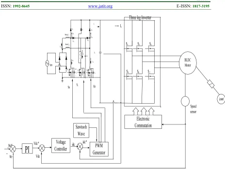
3.1 6-switch VSI fed BLDC motor drive
Figure 5 shows the block diagram of Interleaved Boost Converter based VSI fed BLDC motor with 6 switch VSI configuration. There are two control loops, one is the speed control loop which is outer loop and another one is inner current loop. The speed error is obtained by comparing the actual speed with the desired reference speed. The speed error is fed to the PI voltage controller to obtain the reference dc link voltage and compared with actual value to produce the current. Gate pulses are obtained for 6-switch VSI through hysteresis current control
technique. As we know that torque ripple of BLDC motor drive is mainly depends on speed and phase current during commutation. The commonly used commutation in 3 phase BLDC motor is the six-step, in which each phase voltage is energized for interval of 1200 electrical according to the rotor electrical
[image:7.612.325.538.258.477.2]position. In this paper, a new circuit topology to achieve dc link voltage control has been proposed to keep phase current changing at the same rate during commutation. The desired commutation voltage accomplished by the interleaved boost converter. The specifications of PMBLDC Motor are given in Table-2.
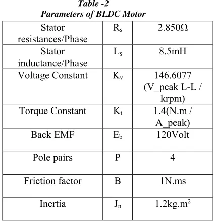
Table -2
Parameters of BLDC Motor Stator
resistances/Phase
Rs 2.850Ω
Stator
inductance/Phase Ls 8.5mH
Voltage Constant Kv 146.6077
(V_peak L-L / krpm) Torque Constant Kt 1.4(N.m /
A_peak)
Back EMF Eb 120Volt
Pole pairs P 4
Friction factor B 1N.ms
3937
Figure 5 Interleaved Boost Converter with six switch three phase VSI fed PMBLDC Motor
The three phase voltage equations of BLDC Motor are as follows
no a a
as
e
V
dt
di
L
V
=
Ri
a
(27)
no b b
bs
e
V
dt
di
L
V
=
Ri
b
(28)
no c c
rs
e
V
dt
di
L
V
=
Ri
c
(29)
Due to the interaction of the current in stator winding and the magnetic field from rotor magnets, the electromagnetic torque of BLDC motor produced as follows:
m c c b b a a e
W
i
e
i
e
i
e
T
=
(30)
Where Wm is the mechanical speed of the rotor .The equation of motion is given by
J
BW
T
T
dt
dW
m e
l
m
(31)
Where Tl = Load torque ,
B = Damping constant ,
J=Moment of inertia of motor and load
For six- step motor control, at each step the instantaneous output power will be will delivered from two phase in series, and is given by
m
e
V
I
T
P
0=
m
2
max(32)
Where ‘I’ is the current amplitude and E is the induced Back EMF .From (30) and (32),the output torque can be also be expressed as
m t
e
K
T
T
2
(33)
Where,Kt is the motor torque constant.The three phase voltage equations can be rewritten as
no a a
V
e
dt
di
L
a
Ri
=
0
3938
b no
b
dc
e
V
dt
di
L
V
=
Ri
b
(35) c no c
V
e
dt
di
L
cRi
=
0
(36))
V
-(
3
1
=
dc maxno
V
V
(37) m m m c c b b a a eW
V
I
W
i
e
i
e
i
e
T
=
2
max(38) s dc a
L
V
V
dt
di
3
2
max
(39) s dc bL
V
V
dt
di
3
)
2
(
2
max
(40) s dc cL
V
V
dt
di
3
4
max
(41)
The time taken for i
ato from the initial value
I
mis
max 1
2
3
V
V
I
L
t
dc m s
(42)
The time taken for i
bto increase from 0 to I
mis
)
(
2
3
max 1V
V
I
L
t
dc m s
(43)
Accordingto(34)(42),andia+ib+ic=0,during
commutation, the electromagnetic torque can be calculated as
)
3
4
(
(
2
=
max max maxs m m e
L
V
V
I
W
V
T
(44)
The relative torque ripple is given by
t
L
V
V
T
T
T
s pre e e e)
3
4
(
=
max
max
(45)
According to (33) and (41)-(44),the following conclusion can be drawn
1.
If Vdc>4Vmax, then t1>t2, and the torque keepsincreasing during commutation .
2. If Vdc>4Vmax, then t1<t2, and the torque keeps
decreasing during commutation. 3.If Vdc>4Vmax, then t1<t2, and the torque is
constant during commutation .
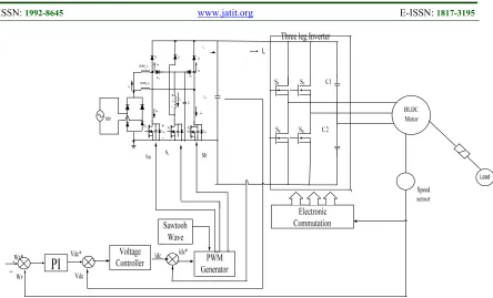
3.4. 4-switch VSI fed BLDC motor
[image:9.612.88.527.71.537.2]3939
Figure 6 Interleaved Boost Converter based 4- switch three phase VSI fed PMBLDC Motor
4. RESULTS AND DISCUSSION
The proposed work has been implemented under
Matlab/Simulink
environment
and
corresponding results are presented for both
6-switch VSI fed BLDC motor and 4-6-switch VSI
fed BLDC motor. Results are taken for different
load torques and speed conditions and relevant
waveforms are presented from figure 7 to figure
10.
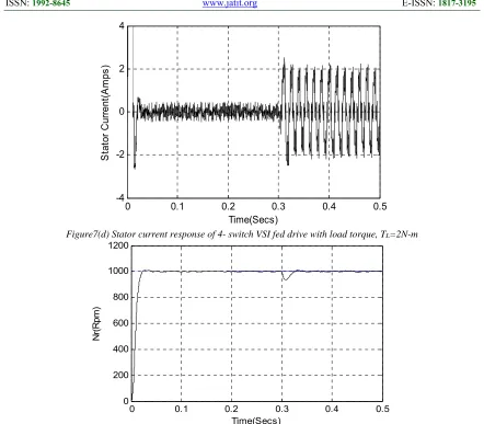
figure 7 shows the performance Analysis of 6-Switch and 4-switch VSI fed PMBLDC Motor for TL=2N-m and 1000rpm,figure 8 shows the
performance Analysis of 6-Switch and 4- switch
VSI fed PMBLDC Motor for T
L=5N-m and
1000rpm.figure 9 shows the performance
Analysis of 6-Switch and 4-switch VSI fed
PMBLDC
3940
0 0.1 0.2 0.3 0.4 0.5
-4 -2 0 2 4
Time(Secs)
T
e(N
-m
)
Figure7(a) Motor torque response of 6-switch VSI fed drive with load torque, TL=2Nm
0 0.1 0.2 0.3 0.4 0.5
-4 -3 -2 -1 0 1 2 3 4
Time(Sec)
T
e(N-m
)
Figur7(b)Motor torque response of 4- switch VSI fed drive with load torque, TL=2N-m
0 0.1 0.2 0.3 0.4 0.5
-4 -2 0 2 4
Time(Secs)
S
tat
or
C
ur
rent
(
A
m
ps
)
3941
0 0.1 0.2 0.3 0.4 0.5
-4 -2 0 2 4
Time(Secs)
S
tat
or
C
ur
rent
(A
m
ps
)
Figure7(d) Stator current response of 4- switch VSI fed drive with load torque, TL=2N-m
0 0.1 0.2 0.3 0.4 0.5
0 200 400 600 800 1000 1200
Time(Secs)
N
r(R
pm
)
Figure 7(e) Speed response of 6-switch VSI fed drive with load torque, TL=2N-m
0 0.1 0.2 0.3 0.4 0.5
0 500 1000 1500 2000 2500
Time(Secs)
Nr
(R
pa
m
)
[image:12.612.125.494.69.281.2]Figure 7(f) Speed response of 4- switch VSI fed drive with load torque, TL=2N-m
[image:12.612.85.527.76.463.2] [image:12.612.168.443.296.462.2]3942
0 0.1 0.2 0.3 0.4 0.5
-10 -5 0 5 10
Time(Secs)
T
e(N
-m)
Figure8(a) Motor torque response of 6-switch VSI fed drive with load torque, TL=5N-m
0 0.1 0.2 0.3 0.4 0.5
-10 -5 0 5 10
Time(Secs)
T
e(N
-m
)
Figure 8(b) Motor torque response of 4- switch VSI fed drive with load torque, TL=5N-m
0 0.1 0.2 0.3 0.4 0.5
-6 -4 -2 0 2 4 6
Time(Secs)
S
tat
or
C
ur
rent
(A
m
ps
)
[image:13.612.158.451.507.690.2]3943
0 0.1 0.2 0.3 0.4 0.5
-6 -4 -2 0 2 4 6
Time(Secs)
S
tat
or
C
ur
rent
(A
m
ps
)
Figure8(d) Stator current response of 4- switch VSI fed drive with load torque, TL=5N-m
0 0.1 0.2 0.3 0.4 0.5
0 200 400 600 800 1000 1200
Time(Secs)
Nr(Rp
m
)
Figure 8 (e) Speed response of 6-switch VSI fed drive with load torque, TL=5N-m
0 0.1 0.2 0.3 0.4 0.5
0 500 1000 1500 2000 2500
Time(Secs)
Nr
(R
pm
)
[image:14.612.96.453.71.282.2]Figure 8(f) Speed response of 4- switch VSI fed drive with load torque, TL=5N-m
[image:14.612.159.453.299.707.2] [image:14.612.158.448.309.498.2]3944
0 0.1 0.2 0.3 0.4 0.5
-4 -2 0 2 4
Time(Secs)
Te
(N
-m
)
Figure 9(a) Motor torque response of 6-switch VSI fed drive with TL= 2N-m and change of speed
0 0.1 0.2 0.3 0.4 0.5
-4 -2 0 2 4
Time(Secs)
Te(
N
-m
)
Figure9 (b) Motor torque response of 4- switch VSI fed drive with TL= 2N-m and change of speed
Figure9(c) Stator current response of 6-switch VSI fed drive with TL=2N-m and change of speed
0 0.1 0.2 0.3 0.4 0.5
-4 -2 0 2 4
Time(Secs)
S
tat
or
C
ur
rent
(A
m
ps
[image:15.612.99.484.74.486.2]3945
0 0.1 0.2 0.3 0.4 0.5
-4 -2 0 2 4
Time(Secs)
S
tat
or
C
urrent
(A
m
ps
)
Figure 9(d) Stator current response of4- switch VSI fed drive with TL=2N-m and change of speed
0 0.1 0.2 0.3 0.4 0.5
0 200 400 600 800 1000 1200
Time(Secs)
Nr
(R
pm
)
Figure 9(e) Speed response of 6-switch VSI fed drive with TL=2N-m and change of speed
0 0.1 0.2 0.3 0.4 0.5
0 500 1000 1500 2000 2500
Time(Secs)
Nr
(R
pm
)
Figure 9(f) Speed response of 4- switch VSI fed drive with TL= 2N-m and change of speed
Figure 9 Performance Analysis of 6-Switch and 4-switch VSI fed PMBLDC Motor for TL=2N-m and change of speed
[image:16.612.92.491.72.275.2] [image:16.612.146.466.296.653.2] [image:16.612.150.461.308.464.2]3946
0 0.1 0.2 0.3 0.4 0.5
-10 -5 0 5 10
Time(Secs)
Te
(N
-m
)
Figure 10(a) Motor torque response of 6-switch VSI fed drive with TL=5N-m and change of speed
0 0.1 0.2 0.3 0.4 0.5
-10 -5 0 5 10
Time(Secs)
T
e(N
-m
)
Figure 10(b) Motor torque response of 4- switch VSI fed drive with TL=5N-m and change of speed
0 0.1 0.2 0.3 0.4 0.5
-6 -4 -2 0 2 4 6
Time(Sec)
S
tat
or
C
urr
ent
(A
m
ps
)
Figure 10(c) Stator current response of 6-switch VSI fed drive with TL=5N-m and change of speed
[image:17.612.89.510.62.630.2] [image:17.612.141.457.444.648.2]3947
0 0.1 0.2 0.3 0.4 0.5
-6 -4 -2 0 2 4 6
Time(Secs)
S
tat
or
C
ur
rent
(A
mps
)
Figure 10(d) Stator current response of 4-switch VSI fed drive with TL=5N-m and change of speed
0 0.1 0.2 0.3 0.4 0.5
0 200 400 600 800 1000 1200
Time(Secs)
Nr(Rp
m
)
Figure10(e) Speed response of 6-switch VSI fed drive with TL=5N-m and change of speed
0 0.1 0.2 0.3 0.4 0.5
0 500 1000 1500 2000 2500
Time(Secs)
Nr
(R
pm
)
Figure 10(f) Speed response of 4- switch VSI fed drive with TL=5N-m and change of speed
Figure 10 Performance Analysis of 6-Switch and 4-switch VSI fed PMBLDC Motor for TL=5N-m and change of speed
[image:18.612.163.441.315.496.2] [image:18.612.154.458.524.690.2]3948
5. CONCLUSION
In this paper, comparison has been made between interleaved boost converter based 6-switch and 4-switch VSI fed PMBLDC motor drive. The performance evaluation of the proposed work is investigated under different operating conditions. From the results, it is observed that transient performance of 6-switch VSI fed PMBLDC motor drive is superior to 4-switch VSI fed PMBLDC motor drive but its steady state response is poor. As for as torque ripple minimization is concerned, the 4-switch VSI fed PMBLDC motor is better compared to 6-switch VSI fed BLDC motor because of less requirement of dc link voltage for 4-switch VSI. The torque ripple depends on dc link voltage of VSI. Number of switches are less in 4 –switch VSI, so, switching losses are also very less.
REFERENCES
[1]J.Yungtaek and M. M. Jovanovic, “Interleaved PFC boost converter with intrinsic voltage-doubler characteristic,” in Proc. IEEE Power Electron.Spec. Conf., Jun. 2006, pp. 1888–1894. [2]G. Yao, A. Chen, and X. He, “Soft switching
circuit for interleaved boost converters,” IEEE Trans. Power Electron., Vol. 22, No. 1, pp. 80– 86, Jan.2007.
[3]Yie-Tone Chen, Shin-Ming Shiu, and Ruey-Hsun Liang, “Analysis and Design of a Zero-Voltage-Switching and Zero-Current-Switching Interleaved Boost Converter,” IEEE Transactions on Power Electronics, Vol. 27, No. 1, Jan. 2012. [4]Ching-Ming Lai , Ming-Ji Yang and Shih-Kun
Liang, “A Zero Input Current Ripple ZVS/ZCS Boost Converter with Boundary-Mode Control,”2014,7,67656782;doi:10.3390/en71067 65 , ISSN 1996-1073.
[5]Fei Yang, Chenguang Jiang, Allan Taylor, Hua Bai, Adam Kotrba, Argun Yetkin, and Arda Gundogan “Design of a High-Efficiency Minimum-Torque-Ripple 12-V/1-kW Three-Phase BLDC Motor Drive System for Diesel Engine Emission Reductions” IEEE Transactions on Vehicular Technology, Vol. 63, No. 7, September 2014.
[6]V.Ramesh, Y.Kusuma Latha “PFC-Based Control Strategies for Four Switch VSI fed BLDC Motor” , Indian Journal of Science and Technology, Vol 8,Issue 16,July 2015.
[7]Vashist Bist , Bhim Singh, “A Unity Power Factor Bridgeless Isolated Cuk Converter-Fed Brushless DC Motor Drive” IEEE Transactions ON Industrial Electronics, Vol.62, No. 7, July 2015.
[8]V.Ramesh,Y. Kusuma Latha, O.Chandra Sekhar” Soft Switching of Interleaved Boost Converter Fed PMBLDC Motor Using PI And Fuzzy Controllers” Journal of Electrical Engineering ,Volume 16/2016–Edition:2
[9]V.Ramesh,Y.Kusuma Latha “A Soft Switching
Control Strategy Based on Interleaved Boost Converter for BLDC Motor Drive”International Journal of Power Electronics and Drive Systems,

![Figure 3(b) Equivalent circuit for Mode-2[t1-t2]](https://thumb-us.123doks.com/thumbv2/123dok_us/8906311.957005/3.612.312.554.303.561/figure-b-equivalent-circuit-for-mode-t-t.webp)
![Figure 3(e) Equivalent circuit for Mode-5[t4-t5]](https://thumb-us.123doks.com/thumbv2/123dok_us/8906311.957005/4.612.82.288.225.569/figure-e-equivalent-circuit-for-mode-t-t.webp)
![Figure 3(f-a) Equivalent circuit for Mode- 6 [t5 –ta]](https://thumb-us.123doks.com/thumbv2/123dok_us/8906311.957005/5.612.80.546.44.730/figure-f-a-equivalent-circuit-mode-t-ta.webp)
![Figure 3(g) Equivalent circuit for Mode-7 [t6 –t7]](https://thumb-us.123doks.com/thumbv2/123dok_us/8906311.957005/6.612.323.524.88.333/figure-g-equivalent-circuit-mode-t-t.webp)