Vol. 3, Issue 11 (November. 2013), ||V1|| PP 49-57
Design and Implementation of low power Floating Point
Multiplier
J. KoteswaraRao, P.Devi Pradeep
M.Tech(VLSI&ES), Department of ECE, GMR Institute of Technology,GMR Nagar,Rajam. Assistant professor, Department of ECE, GMR Institute of Technology, GMR Nagar,Rajam
Abstract: - In this paper we describe an Design and Efficient implementation of an IEEE 754 low power single precision floating point multiplier targeted for Xilinx Virtex-5 FPGA. The multiplier implementation handles the overflow and underflow cases. Rounding is not implemented to give more precision when using the multiplier in a Multiply and Accumulate (MAC) unit. With latency of three clock cycles the design achieves 301 MFLOPs. The multiplier was verified against Xilinx floating point multiplier core.
Keywords: - floating point; multiplication; FPGA; CAD design flow
I. INTRODUCTION
Floating point numbers are one possible way of representing real numbers in binary format; the IEEE 754 [1] standard presents two different floating point formats, Binary interchange format and Decimal interchange format. Multiplying floating point numbers is a critical requirement for DSP applications involving large dynamic range. This paper focuses only on single precision normalized binary interchange format. Fig. 1 shows the IEEE 754 single precision binary format representation; it consists of a one bit sign (S), an eight bit exponent (E), and a twenty three bit fraction (M or Mantissa). An extra bit is added to the fraction to form what is called the significand1. If the exponent is greater than 0 and smaller than 255, and there is 1 in the MSB of the significand then the number is said to be a normalized number; in this case the real number is represented by (1)
Figure 1. IEEE single precision floating point format
Z = (-1S) * 2 (E -Bias) * (1.M) (1)
Where M = m22 2-1 + m21 2-2 + m20 2-3+…+ m1 2-22+ m0 2-23;
Bias = 127.
1
Significand is the mantissa with an extra MSB bit.
Floating-point implementation on FPGAs has been the interest of many researchers. In [2], an IEEE 754 single precision pipelined floating point multiplier was implemented on multiple FPGAs (4 Actel A1280). In [3], a custom 16/18 bit three stage pipelined floating point multiplier that doesn‟t support rounding modes was implemented. In [4], a single precision floating point multiplier that doesn‟t support rounding modes was implemented using a digit-serial multiplier: using the Altera FLEX 8000 it achieved 2.3 MFlops. In [5], a parameterizable floating point multiplier was implemented using the software-like language Handel-C, using the Xilinx XCV1000 FPGA; a five stages pipelined multiplier achieved 28MFlops.
II. FLOATING POINT MULTIPLICATION ALGORITHM
As stated in the introduction, normalized floating point numbers have the form of Z= (-1S) * 2 (E -Bias) * (1.M). To multiply two floating point numbers the following is done:
1. Multiplying the significand; i.e. (1.M1*1.M2)
2. Placing the decimal point in the result 3. Adding the exponents; i.e. (E1 + E2 – Bias)
4. Obtaining the sign; i.e. s1 xor s2
5. Normalizing the result; i.e. obtaining 1 at the MSB of the results‟ significand 6. Rounding the result to fit in the available bits
Consider a floating point representation similar to the IEEE 754 single precision floating point format, but with a reduced number of mantissa bits (only 4) while still retaining the hidden „1‟ bit for normalized numbers:
A = 0 10000100 0100 = 40, B = 1 10000001 1110 = -7.5
To multiply A and B
1. Multiply significand: 1.0100 × 1.1110
00000
10100
10100
10100
10100
1001011000
2. Place the decimal point: 10.01011000 3. Add exponents: 10000100 +10000001 100000101
The exponent representing the two numbers is already shifted/biased by the bias value (127) and is not the true exponent; i.e. EA = EA-true + bias and EB = EB-true + bias And E
A
+ EB
= EA-true
+ EB-true
+ 2 Bias So we should subtract the bias from the resultant exponent otherwise the bias will be added twice. 100000101- 01111111
10000110
4. Obtain the sign bit and put the result together: 10000110 10.01011000
5. Normalize the result so that there is a 1 just before the radix point (decimal point). Moving the radix point one place to the left increments the exponent by 1; moving one place to the right decrements the exponent by 1.
1 10000110 10.01011000 (before normalizing)
1 10000111 1.001011000 (normalized)
The result is (without the hidden bit):
1 10000111 00101100
6. The mantissa bits are more than 4 bits (mantissa available bits); rounding is needed. If we applied the truncation rounding mode then the stored value is: 1 10000111 0010.
III. HARDWARE OF FLOATING POINT MULTIPLIER
A. Sign bit calculation
Figure 2. Floating point multiplier block diagram
B. Unsigned Adder (for exponent addition)
This unsigned adder is responsible for adding the exponent of the first input to the exponent of the second input and subtracting the Bias (127) from the addition result (i.e. A_exponent + B_exponent - Bias). The result of this stage is called the intermediate exponent. The add operation is done on 8 bits, and there is no need for a quick result because most of the calculation time is spent in the significand multiplication process (multiplying 24 bits by 24 bits); thus we need a moderate exponent adder and a fast significand multiplier.
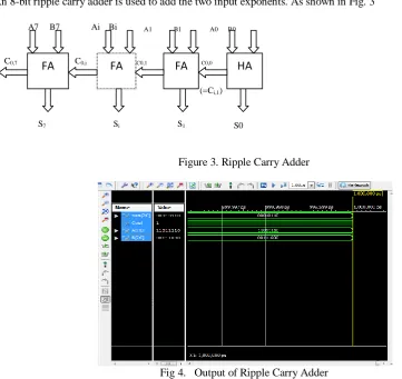
An 8-bit ripple carry adder is used to add the two input exponents. As shown in Fig. 3
A7 B7 Ai Bi A1 B1 A0 B0
C0,7 C0,i C0,1 C0,0
(=Ci,1)
S7 Si S1 S0
Figure 3. Ripple Carry Adder
Fig 4. Output of Ripple Carry Adder
The addition process produces an 8 bit sum (S7 to S0) and a carry bit (Co,7). These bits are concatenated to form a
9 bit addition result (S8 to S0) from which the Bias is subtracted. The Bias is subtracted using an array of ripple
borrow subtractors.
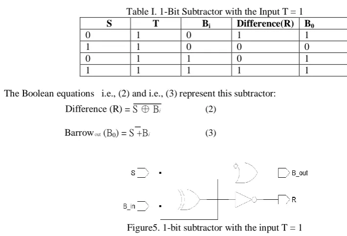
A normal subtractor has three inputs (minuend (S), subtrahend (T), Borrow in (Bi)) and two outputs (Difference (R), Borrow out (Bo)). The subtractor logic can be optimized if one of its inputs is a constant value which is our case, where the Bias is constant (127|10 = 001111111|2). Table I shows the truth table for a 1-bit subtractor with the input T equal to 1 which we will call “one subtractor (OS)”
Table I. 1-Bit Subtractor with the Input T = 1 S T Bi Difference(R) B0
0 1 0 1 1
1 1 0 0 0
0 1 1 0 1
1 1 1 1 1
The Boolean equations i.e., (2) and i.e., (3) represent this subtractor:
Difference (R) = S ⊕ Bi (2)
Barrow out (B0) = S +Bi (3)
Figure5. 1-bit subtractor with the input T = 1
Table II shows the truth table for a 1-bit subtractor with the input T equal to 0 which we will call “zero subtractor (ZS)”
Table II. 1-Bit Subtractor with the Input T = 0
The Boolean equations i.e., (4) and i.e., (5) represent this subtractor:
Difference (R) = S ⊕ Bi (4)
Barrowout (B0) = S +Bi (5)
Figure 6. 1-bit subtractor with the input T = 0
Figure7. Ripple Borrow Subtractor
Fig. 6 shows the Bias subtractor which is a chain of 7 one subtractors (OS) followed by 2 zero subtractors (ZS); the borrow output of each subtractor is fed to the next subtractor. If an underflow occurs then Eresult < 0 and the
S T Bi Difference(R) B0
0 0 0 0 0
1 0 0 1 0
0 0 1 1 1
number is out of the IEEE 754 single precision normalized numbers range; in this case the output is signaled to 0 and an underflow flag is asserted.
Fig8. Output of Ripple Borrow Subtractor
C. Unsigned Multiplier (for significand multiplication)
This unit is responsible for multiplying the unsigned significand and placing the decimal point in the multiplication product. The result of significand multiplication will be called the intermediate product (IP). The unsigned significand multiplication is done on 24 bit. Multiplier performance should be taken into consideration so as not to affect the whole multiplier‟s performance. A 24x24 bit carry save multiplier architecture is used as it has a moderate speed with a simple architecture. In the carry save multiplier, the carry bits are passed diagonally downwards (i.e. the carry bit is propagated to the next stage). Partial products are made by ANDing the inputs together and passing them to the appropriate adder.
Carry save multiplier has three main stages: 1- The first stage is an array of half adders.
2- The middle stages are arrays of full adders. The number of middle stages is equal to the significand size minus two.
3- The last stage is an array of ripple carry adders. This stage is called the vector merging stage.
The number of adders (Half adders and Full adders) in each stage is equal to the significand size minus one. For example, a 4x4 carry save multiplier is shown in Fig9 and it has the following stages:
Figure9. 4x4 bit Carry Save multiplier In Fig. 9:
1- Partial product: aibj = ai and bj 2- HA: half adder
fig 10. Output of Multiplication of Two Significand bits
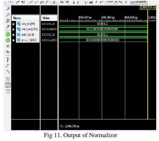
D. Normalizer
1- If the leading one is at bit 46 (i.e. to the left of the decimal point) then the intermediate product is already a normalized number and no shift is needed.
2- If the leading one is at bit 47 then the intermediate product is shifted to the right and the exponent is incremented by 1.
The shift operation is done using combinational shift logic made by multiplexers. Fig. 12 shows a simplified logic of a Normalizer that has an 8 bit intermediate product input and a 6 bit intermediate exponent input.
Fig 11. Output of Normalizer
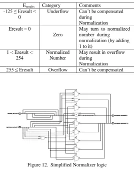
IV. UNDERFLOW/OVERFLOW DETECTION
Table III. Normalization Effect on Result‟s Exponent and Overflow/Underflow Detection
Figure 12. Simplified Normalizer logic
When an overflow occurs an overflow flag signal goes high and the result turns to ±Infinity (sign determined according to the sign of the floating point multiplier inputs). When an underflow occurs an underflow flag signal goes high and the result turns to ±Zero (sign determined according to the sign of the floating point multiplier inputs). Demoralized numbers are signaled to Zero with the appropriate sign calculated from the inputs and an underflow flag is raised. Assume that E1 and E2 are the exponents of the two numbers A and B respectively; the result‟s exponent is calculated by i.e., (6)
Eresult = E1 + E2 - 127 (6)
E1 and E2 can have the values from 1 to 254; resulting in
Eresult having values from -125 (2-127) to 381 (508-127); but for normalized numbers, Eresult can only have the values from 1 to 254. Table III summarizes the Eresult different values and the effect of normalization on it.
V. PIPELINING THE MULTIPLIER
In order to enhance the performance of the multiplier, three pipelining stages are used to divide the critical path thus increasing the maximum operating frequency of the multiplier. The pipelining stages are imbedded at the following locations:
1. In the middle of the significand multiplier, and in the middle of the exponent adder (before the bias subtraction).
2. After the significand multiplier, and after the exponent adder.
3. At the floating point multiplier outputs (sign, exponent and mantissa bits).
Eresults Category Comments
-125 ≤ Eresult < 0
Underflow Can‟t be compensated during
Normalization Eresult = 0
Zero
May turn to normalized number during
normalization (by adding 1 to it)
1 < Eresult < 254
Normalized Number
May result in overflow during
Figure13. Floating point multiplier with pipelined stages
Fig. 13 shows the pipelining stages as dotted lines. Three pipelining stages mean that there is latency in the output by three clocks. The synthesis tool “retiming” option was used so that the synthesizer uses its optimization logic to better place the pipelining registers across the critical path
Fig14. Output of Floating Point Multiplier
VI. IMPLEMENTATION AND TESTING
The whole multiplier (top unit) was tested against the Xilinx floating point multiplier core generated by Xilinx coregen. Xilinx core was customized to have two flags to indicate overflow and underflow, and to have a maximum latency of three cycles. Xilinx core implements the “round to nearest” rounding mode.
TABLE IV. AREA AND FREQUENCY COMPARIS BETWEEN THE IMPLEMENTED FLOATING POINT MULTIPLIER AND
XILINX CORE
Our Floating Point Xilinx Core
Multiplier
Function Generators 1263 765
CLB Slices 604 266
DFF 293 241
Max frequency 301.114 MHz 221.484 MHz
Top Multiplier
Normalizer
Overflow/Underflow detection ddetection
Exponent
Adder Sign
Bit
Significand
Multiplier
Mu
VII. CONCLUSIONS AND FUTURE WORK
In This paper we presents an implementation of a floating point multiplier that supports the IEEE 754-2008 binary interchange format; the multiplier doesn‟t implement rounding and just presents the significand multiplication result as is (48 bits); this gives better precision if the whole 48 bits are utilized in another unit; i.e. a floating point adder to form a MAC unit. Using this floating point multiplier we can get a better accuracy value, so we can get better efficiency. In this project we can use 48 bits using the multiplier section so circuit complexity is more then power consumption is more. So, my extension project is reduce the power consumption as well as better accuracy without changing the circuit behavior.
REFERENCES
[1] IEEE 754-2008, IEEE Standard for Floating-Point Arithmetic, 2008.
[2] B. Fagin and C. Renard, “Field Programmable Gate Arrays and Floating Point Arithmetic,” IEEE Transactions on VLSI, vol. 2, no. 3, pp. 365–367, 1994.
[3] N. Shirazi, A. Walters, and P. Athanas, “Quantitative Analysis of Floating Point Arithmetic on FPGA Based Custom Computing Machines,” Proceedings of the IEEE Symposium on FPGAs for Custom Computing Machines (FCCM‟95), pp.155–162, 1995.
[4] L. Louca, T. A. Cook, and W. H. Johnson, “Implementation of IEEE Single Precision Floating Point Addition and Multiplication on FPGAs,” Proceedings of 83 the IEEE Symposium on FPGAs for Custom Computing Machines (FCCM‟96), pp. 107–116, 1996.
[5] A. Jaenicke and W. Luk, "Parameterized Floating-Point Arithmetic on FPGAs", Proc. of IEEE ICASSP, 2001, vol. 2, pp. 897-900.
[6] B. Lee and N. Burgess, “Parameterisable Floating-point Operations on FPGA,” Conference Record of the Thirty-Sixth Asilomar Conference on Signals, Systems, and Computers, 2002
[7] “DesignChecker User Guide”, HDL Designer Series 2010.2a, Mentor Graphics, 2010
[8] “Precision® Synthesis User‟s Manual”, Precision RTL plus 2010a update 2, Mentor Graphics, 2010.
Author 1 profile:
Mr. Koteswara Rao Junaboyina. Pursuing M.Tech(VLSI&ES) in GMR Institute of Technology, Rajam. Completed B.Tech(ECE) in Naland Institute of Engineering and Technology, kantepudi.
Author 2 profile:
Mr. Devi pradeep podugu. Obtained his M.Tech (VLSI-SD) from National Institute of Technology, Warangal. Completed B.Tech (ECE) in VITAM College of Enggineering, Visakhapatanam. Now working as Assistant Professor in GMR Institute of Technology, Rajam. Having 7 years of teaching experience. He is Life Member of IETE.