Design of Open Core Protocol (OCP) IP Block
using VHDL
Vinay Dhok Prof. Mrs. Pooja Thakre
Student H. O. D Department of Electronics and Telecommunication
Engineering
Department of Electronics and Telecommunication Engineering
Nuva College of Engineering and Technology, Nagpur, Maharashtra, India
Nuva College of Engineering and Technology, Nagpur, Maharashtra, India
Abstract
The Open Core Protocol (OCP) is a core centric protocol which defines a high-performance, bus-independent interface between IP cores. It reduces design time, design risk, and manufacturing costs for SOC designs. Main property of OCP is that it can be organized with respect to the application required. The OCP is chosen because of its advanced supporting features such as configurable sideband, control signaling and test harness signals, when compared to other core protocols. The OCP defines a point-to-point interface between two communicating entities such as IP cores and bus interface modules. One entity acts as the master of the OCP instance, and the other as the slave. Only the master can present commands and is the controlling entity. The slave responds to commands presented to it, either by accepting data from the master, or presenting data to the master. For two entities to communicate there need to be two instances of the OCP connecting them such as one where the first entity is a master and one where the first entity is a slave. In this work, the various OCP profiles will be designed using VHDL and the developed design can be used with respect to its suitable application in the real time product. Basically the OCP unifies all inter-core communications. The OCP’s synchronous unidirectional signaling produces simplified core implementation, integration and timing analysis. The OCP readily adapts to support new core capabilities while limiting test suite modifications for core upgrades.
Keywords: OCP Bridge Master; Slave; OCP compliant; Interface; Power Analysis; Power reduction; Multi voltage Design ________________________________________________________________________________________________________
I. INTRODUCTION
The Open Core Protocol (OCP) is a core centric protocol which defines a high-performance, bus-independent interface between IP cores that reduces design time, design risk, and manufacturing costs for SOC designs. Main property of OCP is that it can be configured with respect to the application required. The OCP is chosen because of its advanced supporting features such as configurable sideband control signaling and test harness signals, when compared to other core protocols.
The other bus and component interfaces address only the data flow aspects of core communications, the ocp unifies all inter-core communications, including sideband control and test harness signals. The OCP’s synchronous unidirectional signaling produces simplified core implementation, integration, and timing analysis. The OCP readily adapts to support new core capabilities while limiting test suite modifications for core upgrades.
The Open Core Protocol™ (OCP) defines a high-performance, bus-independent interface between IP cores that reduces design time, design risk, and manufacturing costs for SOC designs. An IP core can be a simple peripheral core, a high-performance microprocessor, or an on-chip communication subsystem such as a wrapped on-chip bus. The Open Core Protocol,
Achieves the goal of IP design reuse. The OCP transforms IP cores making them independent of the architecture and design of the systems in which they are used
Optimizes die area by configuring into the OCP only those features needed by the communicating cores
Simplifies system verification and testing by providing a firm boundary around each IP core that can be observed, controlled, and validated
The approach adopted by the Virtual Socket Interface Alliance’s (VSIA) Design Working Group on On-Chip Buses (DWGOCB) is to specify a bus wrapper to provide a bus-independent Transaction Protocol-level interface to IP cores. The OCP is equivalent to VSIA’s Virtual Component Interface (VCI). While the VCI addresses only data flow aspects of core communications, the OCP is a superset of VCI additionally supporting configurable sideband control signaling and test harness signals. The OCP is the only standard that defines protocols to unify all of the inter-core communication.
OCP eliminates the task of repeatedly defining, verifying, documenting and supporting proprietary interface protocols. The OCP readily adapts to support new core capabilities while limiting test suite modifications for core upgrades. Clearly delineated design boundaries enable cores to be designed independently of other system cores yielding definitive, reusable IP cores with reusable verification and test suites.
Any on-chip interconnects can be interfaced to the OCP rendering it appropriate for many forms of on-chip communications: Dedicated peer-to-peer communications, as in many pipelined signal processing applications such as MPEG2 decoding. Simple slave-only applications such as slow peripheral interfaces.
High-performance, latency-sensitive, multi-threaded applications, such as multi-bank DRAM architectures.
The OCP supports very high performance data transfer models ranging from simple request-grants through pipelined and multi-threaded objects. Higher complexity SOC communication models are supported using thread identifiers to manage out-of-order completion of multiple concurrent transfer sequences.
The Open Core Protocol interface addresses communications between the functional units (or IP cores) that comprise a system on a chip. The OCP provides independence from bus protocols without having to sacrifice high-performance access to on-chip interconnects. By designing to the interface boundary defined by the OCP, you can develop reusable IP cores without regard for the ultimate target system.
Given the wide range of IP core functionality, performance and interface requirements, a fixed definition interface protocol cannot address the full spectrum of requirements. The need to support verification and test requirements adds an even higher level of complexity to the interface. To address this spectrum of interface definitions, the OCP defines a highly configurable interface. The OCP’s structured methodology includes all of the signals required to describe an IP cores’ communications including data flow, control, and verification and test signals.
Here the importance of project comes into picture i.e. “OCP (Open Core Protocol) plays a vital role by doing its transaction between two different IP cores, which will make the application fail when it doesn’t work properly”.
II. LITERATURE SURVEY
With the rapid progress of system-on-a-chip (SOC) and massive data movement requirement, on-chip system bus becomes the central role in determining the performance of a SOC. Two types of on-chip bus have been widely used in current designs: pipelined-based bus and packet-based bus.
For pipelined-based buses, such as ARM’s AMBA 2.0 AHB, IBM’s Core Connect and Open Core’s Wishbone, the cost and complexity to bridge the communications among on-chip designs are low. However, pipeline-based bus suffers from bus contention and inherent blocking characteristics due to the protocol. The contention issue can be alleviated by adopting multi-layer bus structureor using proper arbitration policies. However, the blocking characteristic, which allows a transfer to complete only if the previous transfer has completed, cannot be altered without changing the bus protocol. This blocking characteristic reduces the bus bandwidth utilization when accessing long latency devices, such as an external memory controller.
To cope with the issues of pipelined-based buses packet-based buses such as ARM’s AMBA 3.0 AXI, OCP-IP’s Open Core Protocol (OCP), and STMicroelectronics’ ST Bus have been proposed to support outstanding transfer and out-of-order transfer completion. We will focus on AXI here because of its popularity. AXI bus possesses multiple independent channels to support multiple simultaneous address and data streams. Besides, AXI also supports improved burst operation, register slicing with registered input and secured transfer.
Despite the above features, AXI requires high cost and possesses long transaction handshaking latency. However, a shared-link AXI interconnect can provide good performance while requiring less than half of the hardware required by a crossbar AXI implementation. This work focused on the performance analysis of a shared-link AXI. The handshaking latency is at least two cycles if the interface or interconnect is designed with registered input. This would limit the bandwidth utilization to less than 50%. To reduce the handshaking latency, we proposed a hybrid data locked transfer mode. Unlike the lock transfer in which requires arbitration lock over transactions, our data locked mode is based on a transfer-level arbitration scheme and allows bus ownership to change between transactions. This gives more flexibility to arbitration policy selection.
With the additional features of AXI, new factors that affect the bus performance are also introduced. The first factor is the arbitration combination. The multi-channel architecture allows different and independent arbitration policies to be adopted by each channel. However, existing AXI-related works often assumed a unified arbitration policy where each channel adopts the same arbitration policy. Another key factor is the interface buffer size. A larger interface buffer usually implies that more out-of-order transactions can be handled. The third factor is the task access setting, which defines how the transfer modes should be used by the devices within a system
III. DESIGN OF OPEN CORE PROTOCOL
The slave responds to commands presented to it, either by accepting data from the master, or presenting data to the master. For two entities to communicate there need to be two instances of the OCP connecting them such as one where the first entity is a master, and one where the first entity is a slave.
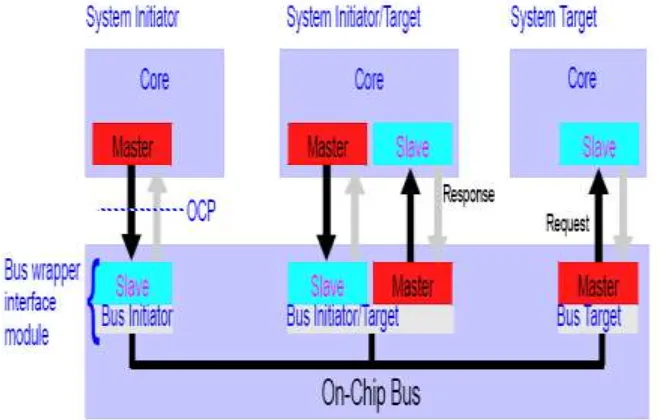
Fig. 1: Basic block diagram of OCP instance
Figure.1 shows a simple system containing a wrapped bus and three IP core entities such as one that is a system target, one that is a system initiator, and an entity that is both. The characteristics of the IP core determine whether the core needs master, slave, or both sides of the OCP and the wrapper interface modules must act as the complementary side of the OCP for each connected entity. A transfer across this system occurs as follows.
A system initiator (as the OCP master) presents command, control, and possibly data to its connected slave (a bus wrapper interface module). The interface module plays the request across the on-chip bus system. The OCP does not specify the embedded bus functionality. Instead, the interface designer converts the OCP request into an embedded bus transfer. The receiving bus wrapper interface module (as the OCP master) converts the embedded bus operation into a legal OCP command. The system target (OCP slave) receives the command and takes the requested action.
Each instance of the OCP is configured (by choosing signals or bit widths of a particular signal) based on the requirements of the connected entities and is independent of the others. For instance, system initiators may require more address bits in their OCP instances than do the system targets; the extra address bits might be used by the embedded bus to select which bus target is addressed by the system initiator.
The OCP is flexible. There are several useful models for how existing IP cores communicate with one another. Some employ pipelining to improve bandwidth and latency characteristics. Others use multiple-cycle access models, where signals are held static for several clock cycles to simplify timing analysis and reduce implementation area. Support for this wide range of behavior is possible through the use of synchronous handshaking signals that allow both the master and slave to control when signals are allowed to change
The design of the Open Core Protocol starts with the initial study based on which the development of FSM (Finite State Machine) for the various supporting operation after which the development of VHDL for the FSM. The development of the FSM’s are the basic step based on which the design can be modelled. The FSM will ensure and explains the clear operation of the OCP step by step and hence this development will act as a basic step for design.
The notations used while designing the OCP are listed in the TABLE I, TABLE II and TABLE III which are as follows. Table - 1
Input Control Values
Control Notations
Used Command
000 IDL Idle
001 WR Write
010 RD Read
Table - 2
Ocp master Command Value
MCmd Notations Used Command
000 IDL Idle
001 WR Write
010 RD Read
Table - 3 Slave Respones value SResp Notations Used Response
00 NUL No Response
01 DVA Data Valid / Accept
The simple write and read operation in OCP has the mandatory signals whose specification is mentioned in the TABLE II.
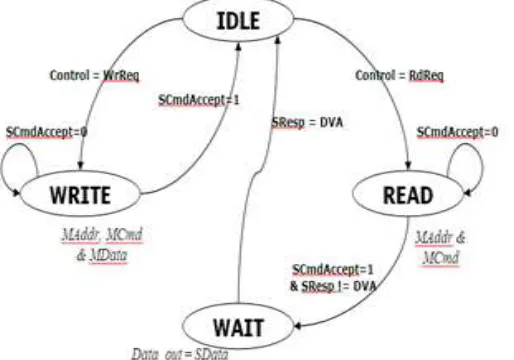
FSM for OCP Master
The Finite State Machine (FSM) is developed for the simple write and read operation of OCP Master. The simple write and read operation indicates that the control goes to IDLE state after every operation. The FSM for the OCP Master – Simple Write and Read is developed and is shown in the Figure 3. Totally there are four states are available in this FSM such as IDLE, WRITE, READ and WAIT.
Basically, the operation in the OCP will be held in two phases. Request Phase
Response Phase
Initially the control will be in IDLE state (Control = “000”) at which all the outputs such as MCmd, MAddr and MData are set to “don’t care”. The system will issue the request to the master such write request which leads to the WRITE state (Control = “001”). In this state, the address and the data will be given to the slave that is to be written and hence the process will get over only when the SCmdAccept is asserted to high. If SCmdAccept is not set, this represents that the write operation still in process and the control will be in the WRITE state itself. Once the write operation is over the control will go to the IDLE state and then it will check for the next request.
When the read request is made, the control will go to the READ state (Control = “010”) and the address is send to the slave which in turn gives the SCmdAccept signal that ends the request phase. Once the SCmdAccept is set and SResp is not Data Valid (DVA), the control will go the WAIT state and will be waiting for the SResp signal. When the read operation is over which represents that the SResp is set to DVA and the data for the corresponding address is taken. Hence the SResp signal ends the response phase and the control will go the IDLE state, then checks for the next request.
Fig. 3: FSM for OCP slave - simple write and read
FSM for OCP Slave
The FSM for the OCP Slave which has the simple write and read operation is developed and is shown in the Figure 3. The slave will be set to the respective state based on the MCmd issued by the master and the output of this slave is that the SCmdAccept and SResp. Initially control will be in the IDLE state and when the master issues the command as write request, and then the control will go the WRITE state in which the data will be written to the corresponding memory address location which is sent by the masters. Once the write operation is finished, the SCmdAccept signal is set to high and is given to the master. When MCmd is given as read request, then the control will move to the READ state in which the data will read from the particular memory address location that is given by the master. Hence the SCmdAccept is set to high and the SResp is set to the DVA which represents that the read operation over and control goes to the IDLE state.
IV. PROPOSED WORK
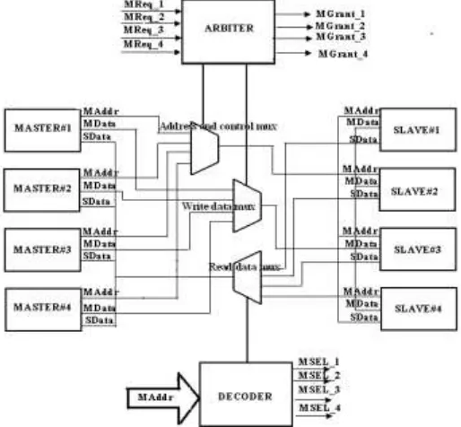
The architecture of the proposed on-chip bus is illustrated in Figure.4, where we show an example with two masters and two slaves. A crossbar architecture is employed such that more than one master can communicate with more than one slave simultaneously. If not all masters require the accessing paths to all slaves, partial crossbar architecture is also allowed. The main blocks of the proposed bus architecture are described next.
Arbiter
Decoder
Since more than one slave exists in the system, the decoder decodes the address and decides which slave return response to the target master. In addition, the proposed decoder also checks whether the transaction address is illegal or nonexistent and responses with an error message if necessary.
FSM-M & FSM-S
Depending on whether a transaction is a read or a write operation, the request and response processes are different. For a write transaction, the data to be written is sent out together with the address of the target slave, and the transaction is complete when the target slave accepts the data and acknowledges the reception of the data. For a read operation, the address of the target slave is first sent out and the target slave will issue an accept signal when it receives the message. The slave then generates the required data and sends it to the bus where the data will be properly directed to the master requesting the data. The read transaction finally completes when the master accepts the response and issues an acknowledge signal. In the proposed bus architecture, we employ two types of finite state machines, namely FSM-M and FSM-S to control the flow of each transaction. FSM-M acts as a master and generates the OCP signals of a master, while FSM-S acts as a slave and generates those of a slave. These finite state machines are designed in a way that burst, pipelined, and out-or-order read/write transactions can all be properly controlled.
V. SIMULATION RESULT
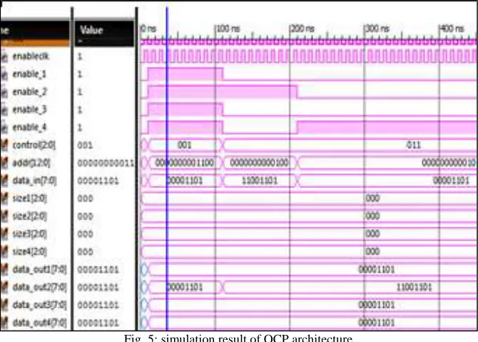
In this work, we use multiple masters and multiple slaves to perform open core protocol data transfer. Simulation waveform shows the data transfer between two cores. Figure.5 shows the simulation with multiple masters and multiple slaves.
Fig. 5: simulation result of OCP architecture
Simulation result shows data transfers to the respective slave when enable signal is enabled. When all enables are ‘high’ then data is transferred to all slave. That is one mater can transfer data to all slaves. We can transfer the data to one or more slave by giving ‘high’ to enable signal.
VI. CONCLUSION
In this paper, the OCP architecture with multiple masters and multiple slaves shows data transfer between master and slave. We can transfer the data to multiple slaves with a delay of 4.310ns which is very less as compared to other core protocols. Our architecture requires less area with high speed which is important factors in system-on-chip (SoC) protocols. In this work, we can also include burst transaction make it flexible with multiple transaction.
REFERENCES
[1] “Open Core Protocol Specification 3.0”, International Partnership, 2000- 2009 OCP-IP Association, Document Revision 1.0.
[2] Chih-Wea Wang, Chi-Shao Lai, Chi-Feng Wu, Shih-Arn Hwang, and Ying-Hsi Lin, “On-chip Interconnection Design and SoC Integration with OCP”,
Proceedings of VLSI-DAT, 2008, pp. 25– 28, April 2008.
[3] “Using the I2C Bus”, I2C tutorial, Robot Electronics http://www.robot-electronics.co.uk/acatalog/I2C_Tutorial.html.
[5] “Computer Architecture and Engineering”, Lecture 8, Designing a Multicycle Processor, www.mips.com.
[6] David A. Patterson, John L.Hennessy, “Computer Organization and Design”, Third Edition, Morgan Kaufmann Publishers, pp.318-339.
[7] Shihua Zhang, Asif Iqbal Ahmed and Otmane Ait Mohamed, “A Reusable Verification Framework of Open Core Protocol”, Circuits and Systems and TAISA
Conference, 2009, pp. 1-4, june 28,2009.
[8] W.-D. Weber, “Enabling reuse via an IP core-centric communications Protocol”, In Proc. IP 2000 System-on-Chip Conference, pages 217-224, Mar 2000.
[9] Prashant D. Karandikar, “Open Core Protocol (OCP) An Introduction to Interface Specification”, 1st Workshop on SoC Architecture, Accelerators & Workloads Jan 10 2010.
[10] Chien-Chun (Joe) Chou, Konstantinos Aisopos, David Lau, Yasuhiko Kurosawa and D. N. (Jay) Jayasimha, “Using OCP and Coherence Extensions to
Support System-Level Cache Coherence”, Technical Paper, pg. nos.10, April 2009.
[11] OCP-IP, “Open core protocol international partnership,” http://www.ocpip.org/,2007.
[12] JamesAldis, “Use of OCP in OMAP 2420”, http://www.ocpip.org/,2005.
[13] Qiang Ma and Evangeline F. Y. Young, Multivoltage Floor Plan Design, IEEE transactions on computer-aided design of integrated circuits and systems, vol.
29, no. 4, April 2010 607.
[14] Bhakthavatchalu R,Deepthy G.R.,Shanooja S,” Implementation of reconfigurable Open Core Protocol compliant memory system using VHDL” Industrial
and Information Systems (ICIIS), 2010 International Conference ,2010,pp.213-218 ,July 29,2011.
[15] Ramesh Bhakthavatchalu, Deepthy G.R,Vidhya S,Nisha V,” Design and Analysis of Low power Open Core Protocol Compliant Interface using VHDL”