ISSN (e): 2250-3021, ISSN (p): 2278-8719
Vol. 09, Issue 5 (May. 2019), ||S (VI) || PP 67-74
Design of A Low Power Area Optimized 4-Bit Arithmetic Logic
Unit for High Speed Processors
Ashish Thakare
1, Sunil Gupta
2, Dr. Pravin Zode
31
PG Scholar, 2Associate Professor, 3Assistant Professor
1,2Department of Electronics / E&TC Engineering, JDCOEM, Nagpur, Maharashtra, India 3Department of Electronics Engineering, YCCE, Nagpur, Maharashtra, India
Abstract:
With the advancement in technology area, power and speed had become a major concern for the growing VLSI industry. Static CMOS logic does not fully meet the needs of future computing. Therefore improved digital logic techniques and styles which are energy efficient, fast and consume lesser area must be utilized. In this paper, a low power, area optimized and high speed 4-Bit Arithmetic Logic Unit having minimum circuit complexity is presented in an elegant way. The major components of the ALU are designed using Modified Gate Diffusion Input (MGDI) technique. The proposed ALU is designed using Cadence Virtuoso tool in 90nm process technology. The simulations are conducted using the Spectre simulation tool at a supply voltage of 1.8V. The simulation results show that the proposed design has lower delay, consumes less power and requires less area.Keywords:
GDI, MGDI, ALU, Power, Delay.I.
Introduction
In the era of growing technology and scaling of devices up to nanometer regime, the demand for low power and high speed microelectronic devices has come to the forefront. Nowadays there is a rapid increase in the utilization of portable applications which demands small-size, low power, high speed and high throughput circuitry. One of the most important parts of a digital processor is the arithmetic logic unit. ALU is designed to do the arithmetic and logic operations which are the basic processes that need to be done for almost any data that is being processed by central processing unit (CPU). And that‟s why the ALU is called heart of microprocessor, microcontroller and digital signal processor. The performance of high speed processing system completely depends on the performance of the ALU and hence it is required that for faster calculations the ALU must be fast. In this paper, a 4-Bit ALU has been designed using a low power 8T hybrid full adder. The sub-circuits i.e. multiplexers, OR Gate, AND gate and inverter are designed using the MGDI technique which requires lesser transistor count.
The paper is organized as follows: Section II gives an overview of previous works done. Section III gives a brief account of Gate Diffusion Input (GDI) technique and Modified Gate Diffusion Input (MGDI) technique. In section IV the components that are required to construct the ALU and its operations are explained. Section V shows the simulation results and performance analysis of the proposed ALU. Section VI concludes the paper.
II.
Previous Works
III.
Overview of GDI And MGDI Techniques
This section gives a brief description of Gate Diffusion Input (GDI) technique and Modified Gate Diffusion Input (MGDI) technique.
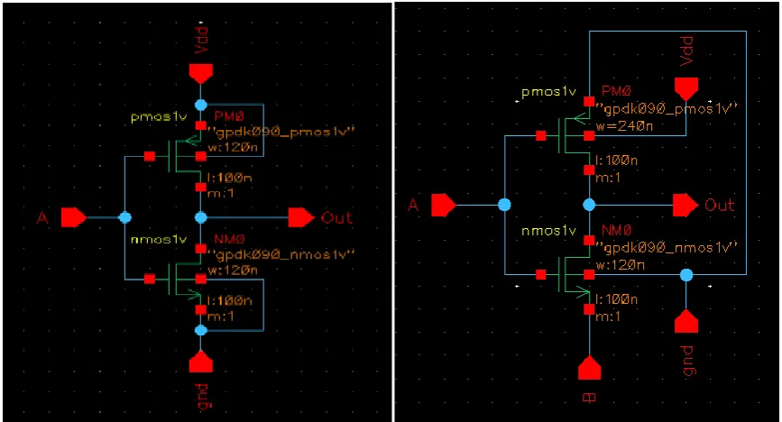
3.1. Gate Diffusion Input (GDI) Technique
The structure of GDI cell was first proposed by Morgenshtein [8]. GDI is a new technique of realizing CMOS static logic technique, which is based on the use of a simple cell structure as shown in fig. 1. This technique is used in digital combinational circuit cell design because of its low power consumption and minimum area on the chip. At first sight a GDI cell looks similar to that of a standard CMOS inverter but there are only few differences. In the place of VDD and GND pins, input signals are used which makes it more flexible than CMOS design. The GDI cell has three inputs namely: G- common input to the gate of NMOS and PMOS; N- input to the source/drain of NMOS; P- input to the source/drain of PMOS. Bulks of both PMOS and NMOS are connected to P or N respectively, so it will be self biased at contrast to CMOS inverter
Fig. 1: Basic GDI Cell
3.2. Modified Gate Diffusion Input Technique
The basic MGDI cell as shown in fig. 2 is similar to that of GDI cell which consists of NMOS and PMOS containing four terminals: „G‟ is the common gate input of NMOS and PMOS transistors, „P‟ is the outer diffusion node of PMOS transistor, „N‟ is the outer diffusion node of MOS transistor, and „Out‟ is the common diffusion node of both transistors.
Fig. 2: Basic MGDI Cell
In the MGDI cell, the bulk node of PMOS transistor is connected to the supply voltage VDD and the bulk of NMOS transistor is connected to ground (GND). This make the GDI to constant body biasing in modified GDI Cell which in turn increase the stability of the circuit and its loading effect. The MGDI cell uses standard four-terminal NMOS and PMOS transistors and can be effortlessly implemented in all type of standard CMOS technology.
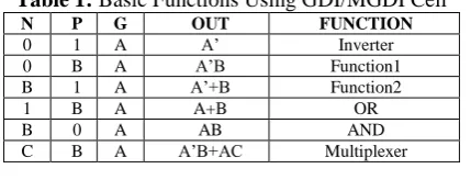
Table 1: Basic Functions Using GDI/MGDI Cell
N P G OUT FUNCTION
0 1 A A‟ Inverter
0 B A A‟B Function1
B 1 A A‟+B Function2
1 B A A+B OR
B 0 A AB AND
Table 1 shows different Boolean operations realized just by changing the control inputs to the cell. A large number of functions can be implemented using the basic GDI/MGDI cell. Function1 (F1) and Function2 (F2) are the universal sets for GDI/MGDI which can be implemented by using only 2 transistors.
IV.
Proposed Work
ALU is one of the most important parts of a digital computer which is designed to do the arithmetic and logic operations that need to be done for almost any data that is being processed by a processor. This section covers the building blocks and the operation of the proposed Design.
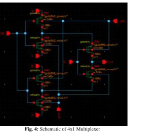
4.1. Multiplexer
Multiplexer is a digital switch which has number of input data lines and a single output line. Selection line plays a major role to select a particular input. There are „2n‟ input lines and „n‟ selection lines whose bit
combinations determine which input is to be transferred to the output. Fig. 3 and fig. 4 represents the schematics of 2x1 multiplexer and 4x1 multiplexer respectively.
4.2. Logic Gates
Logic gates are the building blocks of an ALU which are responsible for all the logical operations in the circuit. The logic block in the proposed circuit consists of AND gate, OR gate, EXNOR gate and an inverter. The schematics of an inverter, AND gate, OR gate and EXNOR gate are shown in fig. 5, fig. 6, fig. 7 and fig. 8 respectively.
Fig. 5: Schematic of an Inverter Fig. 6: Schematic of AND Gate
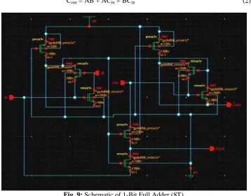
3.4. Full Adder
Full adders are the basic elements of a large number of complex arithmetic circuits like multipliers, dividers, ALUs, etc. Therefore, improvement in the design of full adder circuit results in the overall performance boosting of the entire system. Schematic of the Full Adder (8T) in the proposed design is shown in fig. 9.
A full adder circuit adds binary numbers and accounts for values carried in. A single bit full adder operates on single-bit numbers and adds them. This is generally written as A, B, and Cin. A and B are operands
of the addition operation whereas Cin bit is carried out in from a consequent less significant stage. The circuit
produces a double-bit output i.e. Sum and Carryout (Cout)
where,
Sum = A ⊕ B ⊕ Cin (1)
Cout = AB + ACin + BCin (2)
Fig. 9: Schematic of 1-Bit Full Adder (8T)
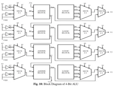
4.4. Design of Proposed 4-bit ALU
The proposed 4-bit ALU design consists of eight 4x1 multiplexers, four 8T full adders, four logic blocks and four 2x1 multiplexers. The output carry Ci + 1 of an earlier stage is feed to the input carry Ci of the
Fig. 10: Block Diagram of 4-Bit ALU
4.5. Operation of Proposed 4-bit ALU
The twelve micro-operations that are performed by the ALU are listed in table 2. The logic operations are selected with the selection line S2 = 0. The input carry Cin has no effect during the logic operations and is
therefore marked with don't care. The arithmetic operations are selected with the selection line S2 = 1.
Table 2: Truth Table for 4-Bit ALU
S2 S1 S0 Cin Micro-Operation Function
0 0 0 x A ˅ B OR
0 0 1 x A ʘ B XNOR
0 1 0 x A ˄ B AND
0 1 1 x A B XOR
1 0 0 0 A‟ + B Subtraction with borrow
1 0 0 1 A‟ + B + 1 Subtraction
1 0 1 0 B Transfer B
1 0 1 1 B + 1 Increment B
1 1 0 0 A + B Addition
1 1 0 1 A + B + 1 Addition with carry
1 1 1 0 B - 1 Decrement B
1 1 1 1 B Transfer B
The arithmetic micro-operations are realized by controlling the data input to the full adder. For the Subtraction operation complement of A is used. The full adder performs this subtraction operation by two‟s complement method. For the Increment and Decrement operations, „logic 1‟ and „logic 0‟ are used as inputs respectively.
Logic micro-operations are performed by the logic block. The outputs of the gates are applied to the data inputs of the 4x1 multiplexer. The selection inputs S1 and S0 opt one of the data inputs of the multiplexer
Fig. 11: Layout of Proposed 4-BIT ALU
The layout of the proposed 4-bit ALU is shown in fig. 11. The layout has been verified by performing all the requisite checks like the DRC checks (Design Rule Check), ERC checks (Extracted Resistance and Capacitance) and LVS checks (Layout versus Schematic) and is free from errors.
V.
Results and Analysis
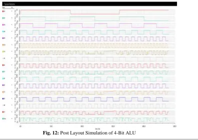
The post layout simulation of the proposed 4-Bit ALU is shown in fig. 12. The simulation is performed in Virtuoso Analog Design Environment (ADE) using Spectre tool with the stop time of 240 ns. For simplification, the input signals A = [A0 A1 A2 A3] and B = [B0 B1 B2 B3] are of constant value throughout the
period i.e., A0 = A1 = A2 = A3 and B0 = B1 = B2 = B3. The ALU performs different operations with the alteration
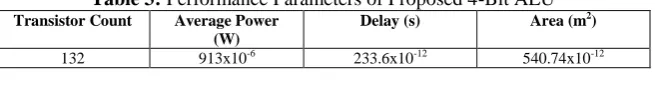
in its control. The overall performance parameters of the proposed 4-Bit ALU using the 90 nm process technology at a supply voltage of 1.8V are shown in table 3.
Table 3: Performance Parameters of Proposed 4-Bit ALU
Transistor Count Average Power (W)
Delay (s) Area (m2)
132 913x10-6 233.6x10⁻¹² 540.74x10⁻¹²
VI.
Conclusion
A low power area optimized 4-Bit ALU designed in 90 nm process technology using the MGDI technique and simulated using the Cadence Virtuoso based Spectre simulator. The hybrid Full adder constructed with only eight transistors utilizing XNOR-XNOR logic and a multiplexer has a better output voltage swing. The proposed design comprises of only 132 transistors and operates at 1.8V supply voltage and has a power consumption of 913μW. The area on chip is 540.74x10⁻¹² m2 and has a delay of 233.6 ps. Overall simulation results shows that the proposed 4-Bit ALU has minimum delay, consumes less power and has less transistor count when compared to other design styles.
References
[1] R. Zimmermann, W. Fichtner, Low power logic styles: CMOS versus pass transistor logic, IEEE Journal of Solid State Circuits 32 (1997) 1079–1090.
[2] Vahid Foroutan, Keivan Navi,and Majid Haghparst, ― A New Low Power Dynamic Full adder Cell Based on Majority Funcion‖IEEE2008.
[3] Raj Lakshmi Shukla, Rajesh Mehra, “Design Analysis and Simulation of 1 bit Arithmetic Logic Unit on different Foundries”,
Proceedings of National Conference on Recent Advances in Electronics and Communication Engineering (RACE-2014), pp.28-29, March 2014.
[4] Srivastava A. and Govindarajan D. “A Fast ALU Design in CMOS for Low Voltage Operation”, VLSI Design, pp. 315-327, 2002.
[5] Akshay Dhenge, Abhilash Kapse, Sandeep Kakde , “Design and Implementation of Area Optimized ALU using GDI Technique”.
International Journal Of Innovative Research In Electrical, Electronics, Instrumentation And Control Engineering,Vol. 2, Issue 3,
March 2014.
[6] T. Esther Rani, M. Asha Rani, Dr. Rameshwar rao, “AREA OPTIMIZED LOW POWER ARITHMETIC AND LOGIC UNIT”
978-1-4244-8679-3/11/$26.00 ©2011 IEEE.
[7] Mukhedkar, M., & Pandurang, W. B. “A 180 nm efficient low power and optimized area ALU design using gate diffusion input technique”, International Conference on Data Management, Analytics and Innovation (ICDMAI), 2017.
[8] A. Morgenshtein, M. Moreinis, and R. Ginosar, "Gate-Diffusion Input (GDI): A Power Efficient Method for Digital Combinatorial Circuits," IEEE Transactions on Very Large Scale Integration (VLSI) Systems, vol. 10, no. 5, pp. pp 566-581, Oct. 2002.
[9] A. Morgenshtein, I. Shwartz, and A. Fish, “Gate Diffusion Input (GDI) logic in standard CMOS Nanoscale process,” 2010 IEEE 26th Convention of Electrical and Electronics Engineers in Israel, 2010.
[10] Padmanabhan Balasubramanian and Johince John, “ Low Power Digital design using modified GDI method”, International