Vol. 53, No. 2, 2005
Optical network and FPGA/DSP based control system
for free electron laser
R.S. ROMANIUK
∗, K.T. PO ´
ZNIAK, T. CZARSKI, K. CZUBA, W. GIERGUSIEWICZ,
G. KASPROWICZ, and W. KOPREK
Institute of Electronic Systems, Warsaw University of Technology 15/19 Nowowiejska Str., 00-665 Warsaw, Poland
Abstract. The work presents a structural and functional model of a distributed low level radio frequency (LLRF) control, diagnostic and telemetric system for a large industrial object. An example of system implementation is the European TESLA-XFEL accelerator. The free electron laser is expected to work in the VUV region now and in the range of X-rays in the future. The design of a system based on the FPGA circuits and multi-gigabit optical network is discussed. The system design approach is fully parametric. The major emphasis is put on the methods of the functional and hardware concentration to use fully both: a very big transmission capacity of the optical fiber telemetric channels and very big processing power of the latest series of DSP/PC enhanced and optical I/O equipped, FPGA chips. The subject of the work is the design of a universal, laboratory module of the LLRF sub-system. The current parameters of the system model, under the design, are presented. The considerations are shown on the background of the system application in the hostile industrial environment.
The work is a digest of a few development threads of the hybrid, optoelectronic, telemetric networks (HOTN). In particular, the outline of construction theory of HOTN node was presented as well as the technology of complex, modular, multilayer HOTN system PCBs. The PCBs contain critical sub-systems of the node and the network. The presented exemplary sub-systems are: fast optical data transmission of 2.5 Gbit/s, 3.125 Gbit/s and 10 Gbit/s; fast A/C and C/A multichannel data conversion managed by FPGA chip (40 MHz, 65 MHz, 105 MHz), data and functionality concentration, integration of floating point calculations in the DSP units of FPGA circuit, using now discrete and next integrated PC chip with embedded OS; optical distributed timing system of phase reference; and 1GbEth video interface (over UTP or FX) for CCD telemetry and monitoring. The data and functions concentration in the HOTN node is necessary to make efficient use of the multigigabit optical fiber transmission and increasing the processing power of the FPGA/DSP/PC chips with optical I/O interfaces. The experiences with the development of the new generation of HOTN node based on the new technologies of data and functions concentration are extremely promising, because such systems are less expensive and require less labour.
Key words: super conducting cavity control, telemetric signal conversion, FPGA, DSP, optical fiber transmission, FPGA with optical I/O, embedded PC OS, free electron laser, FEL, accelerators.
1. Introduction
The accelerator control system consists of several functional layers. The major control loop connects the electromagnetic field sensors located in the superconducting cavities of the ac-celerator, via the networked photonic and electronic system with the megawatt klystron powering the cavities. The aim of the loop is to stabilize the phase and amplitude of the high power field in the microwave narrowband waveguide against the phase of the injected, pulsed electron beam to be accel-erated. The main system is supplemented by many side sub-systems like: auxiliary measurement channels for S parameters of microwave waveguide with couplers, forward and reflected power in many places of the RF distribution network, finesse and cavity detuning originating from the Lorentz force and mi-crophonics, reference clock signal distribution over the whole machine, exception handling for the system and diagnostics. 1.1. Optical transport and access networks. The next gen-eration LLRF system under construction rests in the large ex-tent on the transmission capacity and configuration flexibility of the future optical access, LAN and transport networks.
Rel-atively simple calculations and development trends in opto-electronics show, that the nearest future will bring multi-terabit flows in a single optical fiber. Optical transport systems ex-ploited now offer single terabits per fiber. The spectral effi-ciency of fiber usage is on the average level 0.1–0.2 bits/s/Hz [1–3]. This flow per fiber is realized, for example, in a 32 TDM channel DWDM system of 40 Gbit/s each. It is justified that these parameters will grow to 20–30 Tbit/s/fiber at the spec-tral efficiency of 0.4 bit/s/Hz. It is expected that the flow of 80 Gbit/s will be standardized soon. Theoretically, the ultimate parameters are approximately: 50 Tbit/s/fiber and 0.5 bit/s/Hz [2]. The fibers to be applied for these systems are of the All-Wave type with perfect V shaped spectral loss characteristic. The usable bandwidth spans form the US via S, C, L up to XL sub-bands (1200–1700 nm or more). The compromise are big-ger allowable losses at both ends of the transparency window (up to 1 dB/km or more) and some changes of the dispersion inside this band [4–5].
The immense transport flows possible in backbone opti-cal networks favour the development of access networks and considerably increase their diversification. Particular solutions of the optical access networks reach for broadband technolo-∗e-mail: [email protected]
gies. The number of practical research solutions increases. New massive applications are at the edge of broad appli-cation, including RFID and localization techniques (place-lab.org). The costs of fast flow multiplexing goes down in LANs, via the application of low cost and massively manu-factured CWDM standard devices. An 8-channel (8×1Gbit/s) CWDM transceiver with VCSEL sources [6] for multimode fiber costs now around 30AC. Even less expensive are the transceivers with LEDs working up to 1 Gbit/s. The standard PC boards are now equipped with 1 GbEth NIC, with reflecto-metric abilities for the connected UTP or optical cables. The LANs use optical 10 Gbit/s Ethernet. The OC-192 devices got much cheaper after the introduction of the next, higher gener-ation of the OC hierarchy. It is expected that the OC-192 tier will evolutionary replace the 1 GbEth in LANs and specialized optical access networks. Then the 80 or 160 Gbit/s will prevail at the level of optical transport.
Massive introduction of low cost CWDM in the LANs in-crease the available flows there up to tens of Gbit/s now and hundreds of Gbit/s in the future. Low cost of CWDM stems from the bigger channel separations. Instead of separations going down the chain 200, 100, 50 and 25 GHz, here one has tens of nm. In the ITU-T optical grid, 100 GHz is equivalent to 0.8 nm. The most popular CWDMs on the market are now 16 channels devices working in the spectral region of 1310–1610 nm. The whole optics is integrated in very small transceiver modules. The channel pitch in the CWDM transceivers is 1000, 500 and 250µm, respectively for 4, 8 and 16 channel systems. The standardized (4–16 filament) CWDM fiber rib-bon is 5 mm wide. The prices per unit for the CWDM are 100 times less than for the DWDM. The CWDM standard is self installable and does not require any form of justation [7]. In some cases, the CWDM is the only method of flow increase (at the backbone and access levels), because the installed fibers are old with high dispersion and cannot carry faster signals. There are also available CWDM devices for trunk applications with F-P resonator based filters and DFB laser sources. The CWDM is a relief from urgent changing of the structural cabling. The manufacturers and vendors of the CWDM are: Finisar, Di-Con Fiberoptics, Fiber-Dyne Lab, Canoga Perkins, Alliance Fiber Optics Products, Fortel Networks, Fibre-Works. The first CWDM products were delivered in 2001 by Blaze and Cognet. 1.2. Requirements for optical networks in HEP experi-ments. The photonic and electronic sub-systems, serving the high energy physics (HEP) experiments, are positioned, in most cases, either in the detectors or in accelerator environ-ments. The operating environment is difficult, since there is up to 4 T magnetic field inside the superconducting detector, and the radiation levels reach up to 100 kGy of ionising dose and a fluence of the order of 2×10¹⁴ particles/cm2over the en-visaged 10 year period of operation (CMS data). These values are for the innermost part of the detector. At the periphery of the experiment the corresponding values are 100 Gy and 1012 particles/cm2. There is a number of additional requirements for the detectors and accelerators sub-systems, like continuous operation at low or elevated temperatures or exposure to other
kind of hostile conditions, decreasing considerably the compo-nents MTBF. Since the radiation levels are different in various parts of the detectors and accelerators, in some cases commer-cial off-the-shelf components may be used, whereas others re-quire more customization. A full-scale custom development is nevertheless excluded because of the costs and the long devel-opment time involved. In the data and trigger links only the transmitter end has to be radiation tolerant, the receivers will be located in the shielded area. Radiation-hard receiver com-ponents are needed for the control links running in the opposite direction [8–9].
During the operation period of the experiment it will be very difficult to replace any degraded or damaged components due to the induced radioactivity inside the accelerator/detector and the overall complexity of the apparatus, hence another im-portant requirement on the data and trigger links is reliability. On the other hand, in an application where such a great number of links is required, the cost per link is obviously an important issue also, as is the power consumption. These requirements are generally not compatible with each other. In some parts of the accelertator/detector there are also stringent space limita-tions that dictate the choice of packaging and connectors [8–9]. The serdes (serialiser-deserialiser) circuits can be im-plemented as separate transmitter and receiver parts or as transceivers that integrate the two functions. The latter config-uration is much more common because of the requirement in the datacom industries for duplex links. More recently, com-ponents that have several transceivers on the same chip have become available, and also some of the newest FPGAs in-clude this kind of functionality in a part of their IO-lines. The first high-speed serdes ICs that entered the market required a 5 V supply and were manufactured in GaAs or bipolar sili-con technology, but manufacturers have increasingly moved towards CMOS technology and low-voltage 3.3V/2.5V sup-ply, reducing the power requirements down to about 700–800 mW/channel for 3.3 V, or to around 400 mW/channel for 2.5 V. The parallel input/output lines of the serdes circuits are usu-ally TTL-compatible, while the serial lines standard is PECL (Positive Emitter Coupled Logic). Emitter coupled logic is a non-saturating digital logic, characterised by high speeds, low noise and the ability to drive low-impedance circuits. The serialiser circuit typically includes parallel-to-serial conversion of a databus 8 or 16 bits wide and a clock syn-thesis circuit that enables the use of a low-speed reference clock. Data encoding has traditionally been done on the pro-tocol IC (in which case the input bus width of the serialiser is 10 or 20 bits), but many manufacturers have now incorporated this functionality into the serdes ICs. Encoding is needed to ensure that the data stream has a sufficient number of tran-sitions to enable clock recovery at the receiver end and to make sure the there are roughly equal numbers of 1-s and 0-s sent to maintain dc-balance. The deserialiser end is usually more complicated. It includes a PLL configured for clock and data recovery from the serial input, serial to parallel conver-sion and frame detection of some kind. The restrictions im-posed by the components on the width of the input data word have to be considered when deciding the data format [8–9].
Fig. 1. Block diagram of the gigabit optical link (GOL) serialiser. CERN documentation (after Ref. 8–9)
Synchronisation is an important issue in HEP accelera-tors and FEL experiments, because it is absolutely vital for preserving the integrity of the data and beam quality (elec-tron, hadron and photon). The commercial serdes components are in many cases the ideal choice. In some cases, a clock manipulation is needed. For example the clock of the LHC accelerator is 40.08 MHz, while some classical serdes chips use a reference clock of some multiple of 62.50 MHz. The Agilent G-link HDMP-1022/24 chipset and its lower power successors HDMP-1032A/34A have been more easily adapt-able in this respect but are less likely to become a widely spread standard than Gigabit Ethernet. Recently several Gi-gabit Ethernet compatible serialisers with a wider range of op-erating frequencies have become available. The Gigabit Eth-ernet component that has raised the biggest interest in the HEP community is the Texas Instruments TLK2501. Sev-eral different groups have built link prototypes based on this component, or the Agilent G-link, and have reported very good BER results of 10−13 and∼ 80ns latency. These two components have also been tested for radiation tolerance by different groups. The results are quite encouraging and in-dicate that both components can be used in the outer parts of the CMS experiment. The link latency is an issue of particular interest for the trigger links. The TLK2501 has a smaller latency and a much shorter synchronization time than the G-link, two frames of 25 µs compared to 2 ms [8]. A gigabit serialiser ASIC with an integrated VCSEL driver circuit has been developed at CERN to fulfill the specific re-quirements of the LHC experiments, Fig. 1 [8]. This com-ponent, called GOL (Gigabit Optical Link), is a good exam-ple of how a conventional 0.25 µm CMOS process can be used to produce radiation tolerant devices using special lay-out practices and error mitigation techniques. The GOL has a gate-all-around transistors and carefully placed guard rings to fight the total dose effects. SEUs (Single Event Upsets) have been reduced by Hamming error detection and correc-tion for the configuracorrec-tion registers and by a triple modular re-dundancy design for the data path and control logic. Since hard-wired pins are guaranteed to stay constant, all config-uration bits that are expected not to change during the
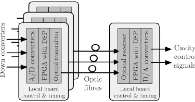
op-eration of the circuit are connected to external pins. The MOS transistor widths have been increased for the serialiser and clock-generation circuits to increase the LET (Linear Energy Transfer) that is required to cause upsets in them. 1.3. Accelerator control system. The TESLA–XFEL pro-ject bases on the nine-cell super conducting niobium res-onators to accelerate electrons and positrons. The accel-eration structure is operated in standing π-mode wave at the frequency of 1.3 GHz. The high power RF oscil-lating field is synchronized with the motion of a parti-cle moving at the velocity of light across the cavity [10]. The low level radio frequency control system (LLRF) [10-12] has been developed to stabilize the pulsed accelerating fields of the resonators, Fig. 2. The control section, pow-ered by one klystron, may consist of many cavities. One klystron supplies the RF power to the cavities through the cou-pled wave-guide with a circulator. The fast amplitude and phase control of the cavity field is accomplished by tion of the signal driving the klystron from the vector modula-tor. The cavities are driven with the pulses of 1.3 ms duration and the average accelerating gradients of 25 MV/m (up to 35 MV/m). The RF signal of each cavity is down-converted to an intermediate frequency of 250 KHz (or recently 81 MHz) pre-serving the amplitude and phase information. The ADC and DAC converters link the analog and digital parts of the system. A very dynamic development of the programmable FPGA circuits, which has been observed during the last years, stimu-lated their wide applications the real-time LLRF systems [13– 16]. The major driving factor behind the widening applica-tions is a considerable lowering of the chip costs relative to the available number of the logical cells, the aggregated ca-pacity of the memory blocks and the aggregated processing power of the inbuilt DSP components. This factor is con-stantly changing the FPGA circuits into the universal building blocks of any advanced photonic and electronic system design. The DSP equipped FPGA chips, when used in the LLRF sys-tem, make possible realization not only the basic functional tasks but also for building of the whole new layers of diag-nostics and communications. The newest generations of the FPGA circuits promise even for more as they have integrated modules of very fast communication interfaces with signal multiplexing and demultiplexing in the direct I/O configura-tion. These I/Os may be either electrical (differential LVDS or PECL) or multi-gigabit optical [17]. The emerging standards are Rocket I/O by Xilinx and SerialLight by Altera [18–19]. The paper debates the structural and functional model of a universal, LLRF control system, for superconduct-ing accelerator, with integrated measurement and diagnos-tic functionalities, which bases on the FPGA chips of the newest generation. The newest predicted features and de-velopment tendencies in the FPGAs were taken into ac-count. It was assumed that the system design should enable a relatively easy and low cost system modifica-tion (hardware upgrade, without physical exchange) for some prolonged period of time after the commissioning.
Fig. 2. General functional block diagram of LLRF Multiple Cavity Control System
Here, the modification capability means the efficient adapta-tion to the changing and extending requirements of the (free electron laser, superconducting cavity) control process. The system should also have the possibility to change the type of the FPGA chip, without rebuilding essentially the framework architecture. After some time of the development it is unavoid-able to change the system generation, but the parameterization and inbuilt flexibility of the design avoids excessive costs of the prototyping process of the LLRF system.
2. Structural and functional model of LLRF
system
The LLRF control system, for the superconducting niobium cavity, may be considered, from the side of the data flow and processing, as a multichannel, synchronous, pipelined hard-ware concentrator, having the following features:
— Multichannel – The need to be multichannel is a fun-damental requirement, because the system is expected to control independently up to several tens of cavities. The multi-parameter field control in the particular cavi-ties requires the presence of nondependent, synchronous readout channels in the system. Some cavity parameters should also be measured by the system to develop its control potential and extend diagnostic capability. The feature of being multichannel enables building of mul-tilevel system. The channels are integrated in a vector sum in the second tier of the system.
— Synchronous – This feature assures a simultaneous (and parallel, in a multichannel system) data processing for the same moment of time, defined by the central system clock of the accelerator. All the system events have to be situated extremely precisely in relation to the accelera-tor clock. The system time perturbations (jitters) have to be taken into account. The perturbations may originate
from the signal jitter, dispersion and attenuation, ences in the length of transmission lines causing differ-ential latencies, unexpected exceptional events, etc. — Pipelined – This design approach stems from the
com-plexity of the used system control procedures and algo-rithms. The signals are numerically processed in consec-utive steps. The data granularity is enabled for the sep-arate moments of time. The data can be distinguished for all channels, all moments of time and all stages of the signal processing in the LLRF control and measure-ment loop. The momeasure-ments are determined by the central system clock of the accelerator, powered by the master oscillator.
Fig. 3. A general functional structure of the data concentration pro-cess in the LLRF control system for superconducting cavity
Taking into account the results of the above considerations, such a system approach to the model design of the LLRF con-trol system as data concentrator is presented in Fig. 3. The data concentration process embraces, in this case, the whole DSP range. It starts from the outputs of the ADCs up to the outputs of the DACs. The signal flow process may be consid-ered in two different categories:
— Functional concentration – The concentration of many functions, in an “almost” single chip system (or re-versely, functional dissipation among a few separate net-worked chips), stems from the properties and complex-ity of the DSP algorithm. The algorithm calculates the results from the multichannel data input in parallel. An example of this feature is that the vector sum is calcu-lated using the parallel data from the ADCs (see Fig. 2). — Hardware concentration – A massive concentration of the hardware processing power in the central node (hub) of the SC cavity LLRF control system is a derivative of the need for the functional concentration. The aim of the hardware concentration is to gather a considerable num-ber of complex physical signals in a single data process-ing object to be treated numerically. An example of this feature is that the structure of many ADCs is connected to a single, powerful enough, FPGA chip.
The design of the, FPGA and photonics based, SC cavity LLRF control system, uses the above features. The design ap-proach considers the system as a distributed data concentrator structure, where the concentration is done for the functional and hardware levels. A simple experimental model of such a system was proposed. It is assumed that the LLRF system would be re-configurable, on considerable scale for functional and hardware levels, in the widest possible extent. The recon-figuration capability embraces the following parameters:
— The number of the input and output channels. The fre-quency of the I/O channel sampling. The frefre-quency of the DSP. The methods of signal processing. The fast reloading of control algorithm.
— Splitting of the pipelined signal processing to the con-centration tiers. The tiers include the functional and hardware levels. The aim of the splitting is to optimize the available (usually scarce) optical transmission band-width and the signal processing rate as well as the sys-tem costs.
Fig. 4. A general functional structure of the (data and functions) con-centration process in the LLRF control system for superconducting
cavity
Figure 4 presents a hardware model of the distributed LLRF system based on the FPGA chips, which are mutually connected via the network of optical links. The realization of this solution is possible due to the new features implemented in the latest series of the programmable circuits. These fea-tures are: the embedded, dedicated DSP blocks of consider-able processing power, large RAM memory and the blocks of serial gigabit transmission. The latter are designed to work di-rectly with the popular and comparatively inexpensive optical fiber multi-gigabit transceivers. From the functional side, the proposed solution enables an easy modification of the system structure. The parameterized structure functions are the num-ber of the input channels and data processing. A standardized and, thus, universal character of the applied fiber optic links enables realization of mutual (direct) functional connections between the particular PCBs. The need of the current system modification may be narrowed to a part of the design, instead of the whole.
3. Parameterization aspects of LLRF system
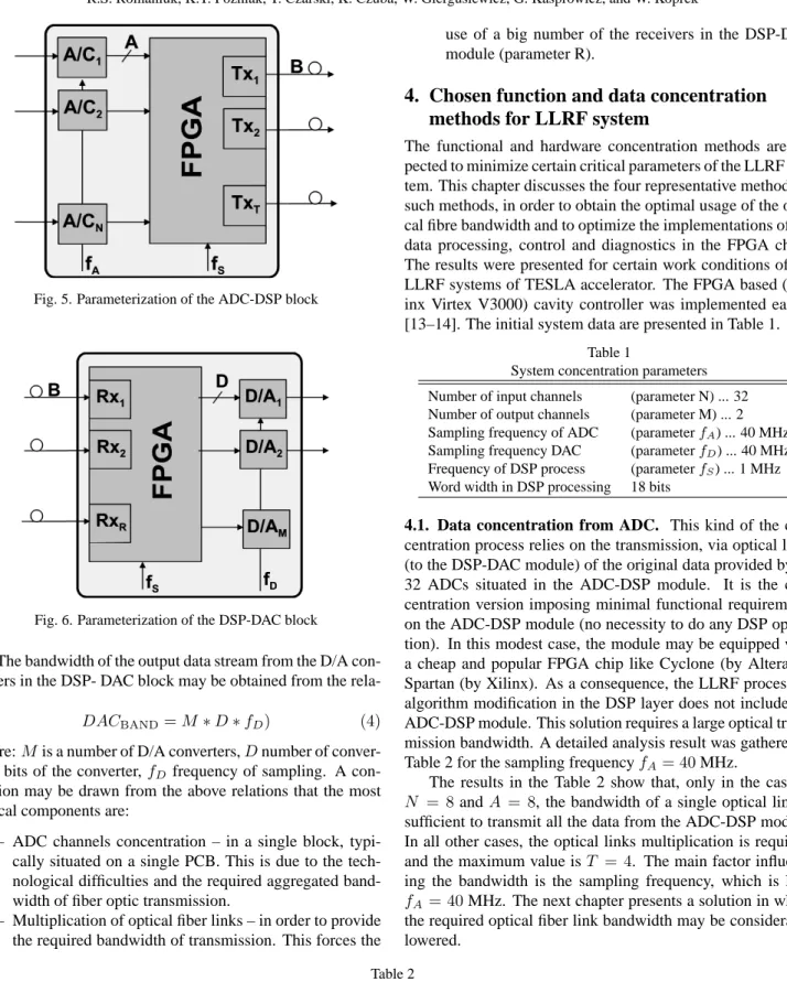
A simple reconfiguration possibility of the LLRF system, pos-tulated in the previous chapter, stems from the elementary (of the low granularity) parameterization of the design. Small, el-ementary, functional blocks are connected via a broadband op-tical fiber network. The opop-tical network is here a universal interface to the fast data distribution. Figures 5 and 6 present the basic parameters of the functional blocks of the LLRF sys-tem and the throughput of the optical network. The bandwidth of the data stream from the ADCs in the ADC-DSP block may be calculated from the following expression:
ADCBAND=N∗A∗fA (1)
where:Nis a number of the ADCs,Ais a number of conver-sion bits of the ADC, andfAis a frequency of the sampling.
Assuming that the full bandwidthADCBANDis distributed to the block DSP-DAC, then, the required optical fiber band-widthT xBANDmust fulfil the following relation:
T xBAND≥ADCBAND⇒(T∗B)≥(N∗A∗fA) (2)
where: T is a number of the required optical fiber channels, andB is the transmission rate expressed in bits/s. The pro-posed solution, in this case, with the multiplication of the op-tical fiber channels (parameterT) stems from the possibility to use some of the FPGA chips with the embedded SERDES blocks. The fast SERDES (serializer/deserializer) modules possess the aggregated throughput of up to 10.5 Gb/s.
The optical fibre receiving link in the DSP-DAC block, possesses, from the assumption, the channels of the same transmission characteristics as the transmitting one. The ag-gregated receiving bandwidth may be calculated from the con-dition:
RxBAND≥C∗T xBAND⇒(R∗B)≥(C∗N∗A∗fA) (3)
where:Cis a number of the ADC-DSP modules connected via the optical fiber network to a single DSP-DAC module.
Fig. 5. Parameterization of the ADC-DSP block
Fig. 6. Parameterization of the DSP-DAC block
The bandwidth of the output data stream from the D/A con-verters in the DSP- DAC block may be obtained from the rela-tion:
DACBAND=M ∗D∗fD) (4)
where:M is a number of D/A converters,Dnumber of conver-sion bits of the converter,fDfrequency of sampling. A
con-clusion may be drawn from the above relations that the most critical components are:
— ADC channels concentration – in a single block, typi-cally situated on a single PCB. This is due to the tech-nological difficulties and the required aggregated band-width of fiber optic transmission.
— Multiplication of optical fiber links – in order to provide the required bandwidth of transmission. This forces the
use of a big number of the receivers in the DSP-DAC module (parameter R).
4. Chosen function and data concentration
methods for LLRF system
The functional and hardware concentration methods are ex-pected to minimize certain critical parameters of the LLRF sys-tem. This chapter discusses the four representative methods of such methods, in order to obtain the optimal usage of the opti-cal fibre bandwidth and to optimize the implementations of the data processing, control and diagnostics in the FPGA chips. The results were presented for certain work conditions of the LLRF systems of TESLA accelerator. The FPGA based (Xil-inx Virtex V3000) cavity controller was implemented earlier [13–14]. The initial system data are presented in Table 1.
Table 1
System concentration parameters Number of input channels (parameter N) ... 32 Number of output channels (parameter M) ... 2 Sampling frequency of ADC (parameterfA) ... 40 MHz
Sampling frequency DAC (parameterfD) ... 40 MHz
Frequency of DSP process (parameterfS) ... 1 MHz
Word width in DSP processing 18 bits
4.1. Data concentration from ADC. This kind of the con-centration process relies on the transmission, via optical links (to the DSP-DAC module) of the original data provided by all 32 ADCs situated in the ADC-DSP module. It is the con-centration version imposing minimal functional requirements on the ADC-DSP module (no necessity to do any DSP opera-tion). In this modest case, the module may be equipped with a cheap and popular FPGA chip like Cyclone (by Altera) or Spartan (by Xilinx). As a consequence, the LLRF processing algorithm modification in the DSP layer does not include the ADC-DSP module. This solution requires a large optical trans-mission bandwidth. A detailed analysis result was gathered in Table 2 for the sampling frequencyfA= 40MHz.
The results in the Table 2 show that, only in the case of N = 8andA = 8, the bandwidth of a single optical link is sufficient to transmit all the data from the ADC-DSP module. In all other cases, the optical links multiplication is required, and the maximum value isT = 4. The main factor influenc-ing the bandwidth is the samplinfluenc-ing frequency, which is here fA = 40MHz. The next chapter presents a solution in which
the required optical fiber link bandwidth may be considerably lowered.
Table 2
Optical transmission bandwidth for chosen parameters of the LLRF system with the indirect concentration method Number of ADC-DSP modules (parameter C) ADC channels (parameter N = 8) ADC channels (parameter N = 16)
Resolution of ADC (parameter A) 8 10 12 14 16 8 10 12 14 16
Standard SERDES transmission (parameter B = 3.125 Gb/s) ParameterT xBAND(Gb/s) 2.56 3.20 3.84 4.48 5.12 5.12 6.40 7.68 8.96 10.24 ParameterT 1 2 2 2 2 2 3 3 3 4 Bandwidth occupancy (%) 81.92 68.27 81.92 95.57 81.92 81.92 81.92 98.30 95.57 93.62 ParameterRxBAND(Gb/s) 10.24 12.80 15.36 17.92 20.48 10.24 12.80 15.36 17.92 20.48 ParameterR 4 8 8 8 8 4 6 6 6 8
Table 3
Optical transmission bandwidth for chosen parameters of the LLRF system in the concentration of modulated I/Q signalsd Number of ADC-DSP modules (parameter C) ADC channels (parameter N = 8) ADC channels (parameter N = 16)
Resolution of ADC (parameter A) 8 10 12 14 16 8 10 12 14 16
Standard SERDES transmission (parameter B = 3.125 Gb/s) ParameterT xBAND(Gb/s) 0.06 0.08 0.10 0.11 0.13 0.13 0.16 0.19 0.22 0.26 ParameterT 1 1 1 1 1 1 1 1 1 1 Bandwidth occupancy (%) 2.05 2.56 3.07 3.58 4.10 4.10 5.12 6.14 7.17 8.19 MaximumfS(MHz) 48.83 39.06 32.55 27.90 24.41 24.41 19.53 16.28 13.95 12.21 ParameterRxBAND(Gb/s) 0.26 0.32 0.38 0.45 0.51 0.26 0.32 0.38 0.45 0.51 ParameterR 4 4 4 4 4 2 2 2 2 2
4.2. Modulated signals concentration I/Q. The concentra-tion of the modulated I/Q signals in the ADC/DSP module enables reduction of the sampling frequency from fA = 40
MHz to fS = 1 MHz for each measurement channel. In
this case, each channel has to possess the independent, pro-grammable correction components. The following parameters are subject to the correction: amplification changes, stabiliza-tion of the reference level, signal averaging block, low-pass filtering, etc. These solutions require the use of the faster and the bigger FPGA circuits than in the previous case. The DSP blocks in these FPGAs are required too. This kind of process-ing serves only for conditionprocess-ing of the measurement signal. It does not embrace within its extent the LLRF control algorithm. This solution leads to the reduction of the required optical fiber bandwidth, what was presented in Table 3 for the sampling fre-quencyfS = 1MHz.
The concentration of the modulated signals I/Q enables normalization (T = 1) of the number of optical fibre trans-mitters for the ADC-DSP modules and the number of optical fiber receivers (R=C) in the DSP-DAC module, which is re-spective to the number of the transmitting modules. The band-width occupancy does not cross the value of 10%, which gives the possibility to increase the I/Q signal modulation frequency from the existing now 250 kHz even to 5 MHz without the ne-cessity to modify the structure of the optical fiber network. The consideration, in a further perspective, of much faster process-ing algorithms, involves the use of very advanced technologi-cally and large, thus expensive, FPGA chips. The next chapters present the solution embracing the process of concentration on the level of the LLRF control algorithm. The tasks fulfilled in a single FPGA chip may be realized in a few smaller chips in the fully distributed processing structure. The structure has an optical network as a backbone.
4.3. I/Q signal concentration after detection. The concen-tration of the I/Q signals after detection in the ADC-DSP mod-ule enables performing of a part of the LLRF control algo-rithm on the level of the ADC-DSP block. The process stores, however, the overall control on each measurement channel in the DSP-DAC module. The considered method of concen-tration requires the use of FPGA circuits equipped with the DSP blocks. The ADC-DSP block may realize a considerable part of the diagnostics and monitoring of the particular chan-nels, apart form doing its regular task of functional processing. In this case, the costs of diagnostics and monitoring imple-mentation may be considerably distributed among a number of FPGA chips. The required optical transmission bandwidth depends on the width of the word used in the DSP algorithm. Table 4 presents the values of the required optical transmis-sion bandwidth for a few exemplary values of the width of DS word.
The method debated in this chapter does not allow for re-ducing the optical transmission bandwidth because the values of I and Q must be transmitted for all channels independently. The further possibility to reduce the transmission bandwidth may be obtained by splitting the control algorithm, what is pre-sented in the next chapter.
4.4. Concentration of local vector sums. A much bigger functional concentration is obtained by performing the calcula-tions of the local vector sum already on the level of the ADC-DSP module. All the control, monitoring and diagnostics of particular channels have to be also implemented in the ADC-DSP module. A much bigger reduction of the optical band-width is obtained, because the vector sums are transferred. The transmission bandwidth depends on the width of the DSP word was presented in Table 5.
Table 4
Optical fibre link transmission bandwidth for chosen parameters of the LLRF system in the concentration method for I and Q signals Number of ADC-DSP modules (parameter C) ADC channels (parameter N = 8) ADC channels (parameter N = 16)
Width of DSP word (bits) 18 24 30 36 42 18 24 30 36 42
Standard SERDES transmission (parameter B = 3.125 Gb/s) ParameterT xBAND(Gb/s) 0.07 0.10 0.12 0.14 0.17 0.14 0.19 0.24 0.29 0.34 ParameterT 1 1 1 1 1 1 1 1 1 1 Bandwidth occupancy (%) 2.30 3.07 3.84 4.61 5.38 4.61 6.14 7.68 9.22 10.75 MaximumfS(MHz) 21.70 16.28 13.02 10.85 9.30 10.85 8.14 6.51 5.43 4.65 ParameterRxBAND(Gb/s) 0.29 0.38 0.48 0.58 0.67 0.29 0.38 0.48 0.58 0.67 ParameterR 4 4 4 4 4 2 2 2 2 2
Table 5
Optical transmission bandwidth for chosen parameters of LLRF system in the method of concentration of local vector sums
The width of DSP word (bits) 18 24 30 36 42
Standard SERDES transmission (parameter B = 3.125 Gb/s) ParameterT xBAND(Gb/s) 0.01 0.01 0.02 0.02 0.02 Bandwidth occupancy (%) 2.29 0.38 0.48 0.58 0.67 MaximumfS(MHz) 173.61 130.21 104.17 86.81 74.40 ParameterRxBAND(Gb/s) 0.02 0.02 0.03 0.04 0.04
5. Universal model of distributed LLRF control
system
The realization of the eventual solution of the distributed LLRF control system basing on the FPGA chips and optical fiber net-work will be preceded by the investigation of the laboratory model. The aim is to create the numerous structures of the system, and investigate the scalability, efficiency and reliabil-ity. The hardware and software layers are subject to practical analysis [15–16] for various models of concentration debated in the previous section.
Figure 7 presents a functional structure of the universal re-search module basing on the FPGA Stratix GX chip by Altera [18]. The module possesses a symmetrical construction and was equipped in:
— four A/D converters (parameterN = 4) of the resolution of 14-bits (parameterA= 14),
— four D/A converters (parameter M = 4) of the resolu-tion of 14-bits (parameterD= 14),
— four optical transmitters (parameterT= 4) of the band-width 3.125 Gb/s (parameterB = 3.125),
— four optical receivers (parameter R = 4) of the band-width 3.125 Gb/s (parameterB = 3.125).
The frequency of the analog channels processing equals to: fA =fD= 40MHz. The frequency of DSP isfS = 1MHz
what is in respect to the requirements of the TESLA-XFEL accelerator.
6. Examples of realized HOTN components
for European FEL
The next generation LLRF control system for the European free electron laser is under intense development, including its functionalities (Sections 2–5) and practical realizations (in this section). The latter materializes in fabrication of successive prototypes, laboratory tests and industrial implementations. During the period 2002–2003 the single-channel prototypes ver. 1 and 2 were tested [14]. The work on eight-channel prototype ver. 3 has been carried out since the beginning of 2004 [20]. The prototype ver. 3.1, on which the work has started since the beginning of 2005, is planned to possess 12 channels and will be fully equipped with multigigabit, multi-channel optical links, DSP coprocessor and embedded Power PC. The prototypes ver. 1 and 2 were tested offline and with the laboratory superconducting cavity Chechia in DESY. The prototype ver. 3 is scheduled for tests on the first accelerator module ACC1 of the VUV FEL. The prototype ver. 3.1 is de-signed for work with linear accelerator in Fermilab and with TTF in DESY.
Fig. 7. A general functional structure of the universal module of the LLRF system
6.1. Access node for HOTN. The access node bases on four software-hardware technologies:
— FPGA programmable circuits of sufficient resources for realization of system algorithms, board management and internal communications,
— inbuilt or discrete micro PC with embedded OS, contain-ing DSP coprocessor for fixed and floatcontain-ing point calcu-lations,
— fast optical transmission for realization of access layer and data transport, together with data concentration in serdes,
— VHDL software for FPGA sub-systems; PC software for embedded OS, applications and GUI.
Figure 8 presents the realized functional block for cooperation between the layers 1, 2 and 4 of the above listed technologies. This is one of the fundamental blocks of the HOTN node. It is used in many operations throughout the node, but is realized in hardware only once.
Fig. 8. The elementary cooperation block of the FPGA chip (logical operations) with DSP/CPU (calculations) and with the I/Os
Table 6 presents exemplary data for the used FPGA chips from two competing families Altera [18] and Xilinx [19]. The available resources allow for realization of efficient network node practically all inside the chip. In case of need the chip reaches for the available auxiliary external resources.
Table 6
Resources of FPGA chips used for building the HOTN node Internal resources Altera StratixGX
EP1SGX40G Xilinx VirtexIIPro XCE2VP100 LCELL 41.250 99.216 Full-duplex gigabit transmission blocks 20 (each 3.125 Gb/s) 20 (each 3.125 Gb/s) RAM memory 3.4 Mb 7.9 Mb Integrated DSP blocks 14 No Multiplication circuits 112 (each 9×9 bits) 444 (each 18×18 bits) Lock circuits 8 12 I/O pins 548 1040
The access node was realized in parameterized form of functional blocks. The blocks were described in VHDL. The implementation was loaded to the FPGA. The board is in the VME standard. The general structure of the board is presented in Fig. 9, for the LLRF system of modular version.
The functional blocks process the data in parallel in the real time. The core of the node are independent modules (may be several), which realize the main algorithm of the measurement-control loop. Here they are System Controller and System Simulator (SIMCON). These blocks reside in the FPGA chip and use inbuilt DSP blocks – fast multiplication circuits. The blocks use data provided by the Programmable Data Con-troller. The preset parameters stem from the algorithms and are described in [10–12]. The module of Input Data Multi-plexer provides programmable choice of control signals for the functional blocks of the HOTN node. Internal, digital feedback loops can be realized, connect external digital and analog sig-nals from the ADC converters or set test vectors programmed and stored in Data Acquisition Block.
The task of the Output Data Demultiplexer is the choice of the signals for DACs or signal registration in Data Acquisition Block. Appropriate configuration of the Input and Output
Mul-tiplexer enables analog feedback between functional modules of the node. The block of Time and Status Controller provides internal synchronization of the node processes. The choice be-tween the internal and external timing is possible, enabling the autonomous work of the node and locally connected de-vices. The block of Communication Controller manages pro-gramming of all blocks from the managing computer system. There are used several I/O protocols for this purpose like EPP, RS, USB, JTAG. The block-hub architecture allows to extract common functionalities in different parts of the node. This leads to considerable simplification of the hardware modules and software based control procedures. The design process embraces smaller number of completely different functionali-ties what lowers the costs and effort.
6.2. Architecture and parameters of PCBs for HOTN. A few versions of the multi-gigabit access nodes to HOTN were realized practically. The board for experimental modular ver-sion was presented in Fig. 10. This figure shows the front and rear sides of this complex solution. It is the model of the broadest hardware reconfiguration possibilities. The system consists of the backbone motherboard (BMB) capable of car-rying up to five mezzanine boards (DB). The small boards real-ize functional, measurement, communication and management devices. Each DB bases on its own FPGA chip. The BMB hardware platform was realized as 20 layers PCB in EURO-6HE standard using VME-BUS. Now, the following DBs are working in the system:
— VME communication module, in slave work mode, us-ing FPGA Acex chip;
— Embedded PC module, equipped in ETRAX CPU (100MHz) and Acex chip,
— Gigabit Optical Transmission module (2.5 Gbit/s) de-signed to concentrate the data streams, possesses the FPGA Cyclone chip and two serdes chips TLK2501, — Board controller, realized on Acex, provides the
follow-ing functionalities: communications with standard exter-nal I/Os; interexter-nal communications with particular mod-ules; distribution of fast control and synchronization sig-nals for all modules and the system as a whole; The slots A-D possess fast direct connections.
Fig. 9. Large amount of measurement data concentration in the HOTN node for control purposes. Block diagrams. Multi-board solution with optical fibre network (left); single bard solution with the converters residing on the same board as FPGA chip (right)
Fig. 10. Backbone Motherboard construction for the modular board solution for the LLRF system
Fig. 11. Backbone Motherboard (BMB) with mezzanine boards, front side view and tests in the VME crate; the BMB is a platform for modular version solution of the TESLA control system
Fig. 12. Eight channel mezzanine bard for the central node of the HOTN (left) and BMB tested in 8-channel configuration in the VME carte (right)
— Common Power Supply module, provides all typical voltages to the slots, FPGA chips, buffers, converters and analog components;
— Analog Data Concentrator module, with multichannel optical data links, each 2.5 Gb/s for 16, 32 and more analog channels, serializers, user’s a ccess via VME or PC (Ethernet, EPP, USB), Stratix GX chip;
— Node Controller module in single channel solution or multichannel solution, possessing VirtexII V4000 chip with hardware DSP blocks, 8 AD channels and 4 DA channels.
The BMB with 2×2 input gigabit opto-board module and VME, Embedded PC modules was presented in Fig. 11, stan-dalone and during tests in the VME crate. This board started the work with a single channel SIMCON. After development of 8-channel SIMCON, the BMB was adapted to work as the fully operational 8-channel node controlling 8 superconduct-ing cavities. The eight channel mezzanine board was pre-sented in Fig. 12, standalone and cooperating with the BMB in the VME crate. The internal latency components for analog and digital signals propagating in the eight channel mezzanine board were measured and the results are presented in Fig. 13. 6.3. Fiber-optic link for the RF phase reference distri-bution system for the XFEL and TESLA. The UV Free-Electron Laser (UVFEL) and The TeV-Energy Superconduct-ing Linear Accelerator (TESLA) [21] projects will require phase synchronization of 0.1 ps short term (millisecond), 1 ps
short term (minutes) and 10 ps long term (days). The strin-gent synchronization requirement of 10 fs was given for the X-Ray Free-Electron Laser (XFEL) [21]. To fulfil this require-ment the XFEL may use a fiber laser as reference generator. This requirement applies for a special location, therefore the RF phase reference distribution system developed for UVFEL and TESLA will also be used in the XFEL. The RF phase ref-erence distribution system must deliver phase stable signals to hundreds of stations over a length of 33 km. Long, optical fiber based links are planned to be an important part of the entire distribution system. Table 7 summarizes these data.
Fig. 13. Measured internal latency components in the eight channel mezzanine board
Fig. 14. Block diagram of the long fiber-optic link Table 7
Phase stability requirements for XFEL and TESLA projects
Parameter Requirement
System Length 3 km (XFEL), 33 km (TESLA)
RF Phase Noise (within macropulse−1ms) 0.05◦RMS (at 1.3 GHz)⇒ ∼0.1ps RF Phase Noise (100 ms) 0.15◦RMS (at 1.3 GHz)⇒ ∼0.3ps RF Phase Stability (short term<1minute) <0.05◦
(at 1.3 GHz)⇒ ∼1ps RF Phase Stability (long term) <5◦(at 1.3 GHz)⇒ ∼10ps
RF frequency range 1 MHz – 2.8 GHz
The different types of stability requirements (Table 7) re-late to different sources of phase fluctuations and drifts. The shortest stability type corresponds mainly to phase noise per-formance of the system components. Devices that mainly dic-tate the phase noise level in our system are the Master Oscil-lator (MO) and frequency multipliers. The optical link also influences the phase noise. The main noise source is the laser transmitter. The phase noise performance of the optical link is a complex problem. Here we assume that a good DFB type laser diode with Relative Intensity Noise (RIN) parameter <−130dBc/Hz and a good telecom optical receiver will ful-fil our design requirements. One can improve the phase noise performance of the link by attaching a low noise phase-locked Voltage Controlled Oscillator (VCO) [22–23] at the link out-put. The short and long term stability of the system is mainly influenced by environmental effects like temperature or other physical parameters changes and also by effects due to aging of the system components. Temperature is the most impor-tant source of phase drifts in our link. Typical fiber-optic cable has a phase length vs. temperature coefficient of K = ∼ 10 ppm/◦C. The primary contribution to the temperature coeffi-cient in fiber is the change in the refractive index.
The concept of the feedback system controlling long term phase drifts at the end of the long link has been developed for the NLC project [24]. Figure 14 shows the block diagram of the system suited to the TESLA project needs. Figure 15 shows the applied laser transmitter. The RF signal from the reference generator modulates the light amplitude of a 1550 nm DFB laser which sends the light into the fiber-optic cable. An ad-justable fiber-optic phase shifter is connected in series with the main fiber. Signal travels through the entire link up to the
mir-ror terminating end of the link. Then, reflected, it travels back the same way up to the optical circulator and further to the opti-cal receiver A (further opti-called FO RxA). The RF phase detector measures the phase difference between the stable input signal and the signal reflected by the mirror. If the phase difference changes (drift in long link), the output voltage of the detector changes. The transmitted and reflected optical signals propa-gate at the same speed (system symmetry), so this error voltage carries information of the phase change in the long link fiber. The phase change observed at Fo RxA is twice the change ob-served at Fo RxB. The error voltage is used to adjust the phase length in the phase shifter to decrease the error. The phase at the very end of the link is stabilized by holding the constant level of the detector output voltage.
Fig. 15. Laser transmitter applied for optical phase stability measur-ments
Fig. 16. The short term phase stability The reflected signal phase is kept stable. By this any
sym-metrical phase error in the system part, right from the optical circulator, can be removed. It also applies to the phase error induced by the frequency change of the RF input signal. Even very small frequency change, which is unavoidable also in high performance oscillators, translates directly to phase drift at the end of long distribution line. The phase drift is the bigger the longer is the distribution line. Our system solves this prob-lem. If the length of the cables connecting the RF input, the fiber-optic laser transmitter (FO Tx), circulator and FO RxA is negligible in comparison with the total length of fiber inside of the phase shifter and in the long link, one can notice that an error observed at the output of FO RxA, caused by RF fre-quency change is also twice the error at the output of FO RxB. Therefore it can be removed by the feedback system. It is a great advantage of the system. The disadvantage is that the phase is controlled only at the mirror for the overall error in the long link. In normal operating conditions one can expect significant local temperature variations along the accelerator tunnel, so one can not make pick up points far from the mir-ror. This scheme can be used for point-to-point link application only. Considering the long term stability, it was found that the main source of phase errors may be the FO Tx and both opti-cal receivers (FO Rx). Let us focus on the FO Tx and RxA. Errors added by these components can not be completely re-moved by the feedback because FO Tx and FO RxA are located asymmetrically in the system. Assume that the only source of phase error is FO Tx. If a phase error ∆ϕTxTx appears in the transmitter, it is transported to the output of the link, so ∆ϕout = ∆ϕTx. The same error appears also at the phase detector input ∆ϕA = ∆ϕTx. To correct this error (make ∆ϕA = 0), the phase length is adjusted in the phase shifter. But since the phase shifter affects the optical signal twice, to correct for−∆ϕA, the phase length adjustment is−0.5∆ϕA in one signal travel direction. Therefore the system will correct the phase at the end of −0.5∆ϕAand the output phase error will be∆ϕout_corrected= ∆ϕTx−0.5∆ϕA = 0.5∆ϕA. The system suppresses errors from laser transmitter and receiver with factor of 2, which already advantage, but it can not re-duce those errors to zero.
A phase control test system was constructed to verify the system performance. The system block diagram differ from the one shown in Fig. 14 with additional phase detector con-nected between the RF signal source and the output of the long link at the mirror. It uses a 20 km spool of single mode fiber
in a temperature controlled oven to simulate the long fiber in the accelerator tunnel. The developed phase detector circuitry operating directly at RF frequency allows avoiding the signal down-conversion and all errors related to that process. The same phase detector type is used in the feedback loop to pro-vide the error voltage for the controller input.
Two versions of the system were tested. One with the phase shifter made of a 5 km fiber on a spool inside of self developed, fast temperature controlled chamber (oven) with a high power thermo electric cooler. The temperature of a spool with 5 km optical fiber can be regulated between 0 and+45◦C. The
over-all time constant of the spool is about 1.2 hour which seems to be sufficient for correcting slow phase changes. This version of the system can operate on very long distribution distances. The second version of the system uses a motorized Optical De-lay Line (ODL) as a phase shifter. A step motor driven device was used with 330 ps phase change range and 40 fs resolution. Because of smaller phase shifter range this system can be used for operation on shorter distribution distances – up to 500 m, e.g. in the TTF2 facility. But there are several advantages of the second solution in comparison to the first one. The most important is a very small dead time and very fast phase change in comparison to the spool inside the oven. It allows for much higher system controller gain without causing feedback loop instability.
The measured phase stability (related to the input signal) at the output of the long link fiber (20 km) for∼1◦C
temper-ature change (feedback switched off) was∼260◦. The phase
length vs. temperature coefficient is calculated to 7 ppm/◦C so it is less than given in the fiber datasheet (10 ppm). The phase change at the output with feedback switched on is shown in Fig. 16, it is 12◦ peak-to-peak and ∼ 2.5◦ after the phase under-shoot (left panel). Several seconds before the phase under-shoot a 1◦C temperature step on the 20 km long link simulator was applied. The phase error was suppressed by the factor of 100. The short term stability, defined as maxi-mum phase difference within last 60 seconds, has been shown in Fig. 16 (right panel). The peak-to-peak value of1.7◦(3.4 ps) does not fulfil design requirement but it can be minimized with faster phase shifter – there is an idea to speed up oven response by using electrical heater made of a grid of wires and a fan blowing air on it. Outside of the disturbance region the short term phase difference is at the level of0.2◦(0.4 ps) which
Fig. 17. Block diagram and PCB photograph of gigabit Ethernet interface for CCD camera (after Ref. 27) The phase stability was also measured for the second
ver-sion of the system – with motorized optical delay line. In this case a 5 km fiber spool inside the oven was used to simulate the long link. A phase error of 300 ps was simulated (to be cov-ered by ODL range of 330 ps). Because of much faster phase shifter, observed was no overshoot as in Fig. 16 and the long phase stability measured was equal0.4◦(0.8 ps) peak-to-peak.
The measurement duration was about 100 hours. In this case phase error was suppressed with a factor of 375 which is a very good value. Obtained short term stability was also excellent – 0.15◦(0.3 ps) peak-to-peak. The result satisfies given stability
requirements.
In the future a series connection of phase shifter made of spool inside the oven and ODL phase shifter is planned. This solution will utilize advantages of both devices. Coverage of very long distribution distance with feedback on phase will be
possible, as well as fast system response to operate with high controller gain and small output signal phase error.
6.4. Gigabit Ethernet interface. A realized gigabit Ethernet interface for CCD camera is another example of functional block for HOTN access. The block diagram and the PCB lay-out of the interface are shown in Fig. 16. The application may range from building a network of cameras, via monitoring through measurements. This particular interface was used for research in astronomy [25,26]. The (electrical or optical) Eth-ernet interface does not possess the confinements of the typi-cal USB solution. The TCP/IP connection makes out of this device a powerful, standalone measurement unit. The unit, in several copies, was practically used in the globally networked research of the optical flashes accompanying gamma ray bursts over the whole sky. The program “πof The Sky” is described
elsewhere [25]. Eventually, the full research network will con-sist of 4 sets of 32 cameras each positioned in four places on the Earth Globe to cover the whole sky.
In order to obtain the transmission rate of 40 ... 100 MB/s, the problem was a choice of proper MAC controller and the physical layer of the link. The RTL9169S-32 controller (Real-tek) was chosen. Ti is a complete MAC circuit with integrated 1000T physical layer. It possesses PCI interface running at 66 MHz. It automatically calculates and verifies the control sums for the upper layers of the TCP/IP/UDP protocols. It results in lower demand for the processing power of the external pro-cessor. The automatic transfer and packet buffering from the external RAM, in BusMaster mode, speeds up the rate. How-ever the PCI interface has to be implemented in the FPGA. The implementation consists of the following blocks [27] (Fig. 17 upper):
— PCI master block provides the communication between the managing microcontroller and the interface. It real-izes transactions of the PCI bus: master read/write, con-figuration read/write. With the aid of this block, the pro-cessor initializes the interface, activates the PCI address space, Busmster mode and configures the register. The PCI master block registers are mapped from the micro-processor side as the external data memory.
— Block PCI slave is a bridge between the PCI and the transmitter and receiver buffers. The interface works in PCI SLAVE mode, during the data transmition from/to the buffers. There were implemented two transmitting buffers (each of them as 1 KB FIFO memory + head-ers) mapped in the address space of the PCI bus. The FIFOs provide fast data transfer (over 200 MB/s). These memories are visible by the PCI interface as a continu-ous address space.
There is 128-byte buffer at the beginning of this address space. The µP places there the TCP/IP/UDP header. The next ad-dresses occupy the FIFO memory, where the right data are lo-cated. The SDRAM memory controller places the data there. There were implemented two full sets of the FIFO transmit-ter buffers, to improve the transfer efficiency. When the first FIFO buffer is filled with data, the TCP/IP header is prepared and written to the second buffer. The MAC controller reads alternately buffers, checks and generates the control sums and sends data via the gigabit interface. This solution has very small demands for the processing power of theµP. Thus, 8-bit
µP is fast enough to provide the implementation of the TCP/IP protocol. The most time consuming part of the protocol (CRC calculation) is realized in the hardware. Additionally, there were implemented transmitter and receiver buffers to send sta-tus mode and commands.
The SDRAM memory controller, which serves the image buffer, has DMA circuit implemented to speed up the trans-fer between the buftrans-fer and FIFOs. Additionally, the SDRAM interface may transmit data to the USB2 interface, which is peripherial circuit of 8051µC. The data are taken to the mem-ory directly from the ADC. The process is synchronized by the CCD sensor charge shift in the control circuit.
The main control block manages the Ethernet and USB transmission. It provides synchronization of data transfer to FIFO buffers in the Ethernet and USB interfaces. The control is done via the register file accessible as external memory of theµP.
The PLL provides the clock signal of 48 MHz for the USB interface, PCI board, DRAM memory and control logic. The interface was realized as a prototype PCI board, Fig. 17 (lower). One PCI connector serves to communicate with giga-bit NIC the other is the edge one. The board features: power supplies, FPGA Cyclone chip, DRAM memory, USB 2.0 inter-face chip and fast 210 MHz, 12bit ADC converter. The board may serve as a very fast frame grabber for analog signals, with PCI/USB interface, USB→PCI bridge and may fulfill other functions. The major aim is to provide the test environment for the GbEth board. In order to confine the amount of labour needed to make the system work, the commercial GbEth PCI board was used. Thus, the software implementation of the in-terface remained the major task.
The chip is controlled by the software executed on the Cy-pressµC FX2. It is the enhanced, fast 8051µP with integrated USB 2.0 interface. It cooperates with the external program me-mory with serial I2C interface. The tasks of the software are:
— PCI board initialization, activation of the memory I/O area;
— board configuration, gigabit Ethernet interface initializa-tion, definition of descriptor addresses;
— preparation of packets to be sent, placing their addresses in the descriptor block, generation of the TCP/IP/UDP header contents;
— decoding and executing incoming commands from both interfaces – Ethernet and USB. These orders may con-cern packets transmission synchronization, status of the device, starting of data acquisition, transmission or set-ting up parameters;
— reaction to errors caused by the PCI board, retransmis-sion of the lost packet;
— theµP serves also as controller and diagnostic device for the whole measurement system cooperating with CCD camera. These functions are: CCD matrix readout con-trol, shutter concon-trol, optical focus motor concon-trol, readout from the temperature and humidity sensors, moisture, configuration of the video signal processor.
The interface was tested and a decision was taken to fabricate a number of copies. The camera with such interface is a pow-erful, standalone, measurement node of the broadband HOTN.
7. Conclusions
The work presents a structural and functional model of a dis-tributed LLRF control system for the TESLA-XFEL accelera-tor. The model bases on FPGA circuits, (DSP and communi-cations functions equipped), and very fast, multigigabit, syn-chronous optical fiber data distribution system. The system design enables uniquely its scaling and realization of various methods of data and processing power concentration on the functional and hardware levels.
The obtained functional solutions lower considerably the required transmission bandwidth for the data. They provide the use of a single optical fiber channel, even at increasing the LLRF control algorithm frequency nearly 20 times. The im-plementation methods of the new LLRF control algorithm, in a distributed version, were described. This implementation re-sults practically in the possibility to distribute the system pro-cessing power into a few smaller FPGA chips.
The solutions, presented in this work, allowed preparing a universal model of the hardware module for the SC cavity, LLRF control system. The module enables building of a fully scalable system structure in a broad range of technical func-tions and parameters. The debated functional and hardware concentration ideas were realized practically and are subject to further investigations of their practical performance. Some de-tails of technological solutions of HOTN subassemblies were presented. There were given some examples of practical ap-plications of HOTN subsystems. The obtained design results and laboratory tests acknowledge that the application of the FPGA chips with optical transmission may redefine the role of DSP chips for complex networked system algorithm realiza-tion. The new generations of programmable matrices possess direct optical access to the pads. Now these are the following interfaces: Rocket I/O in the Virtex II and DirectLight in the Stratix GX. The future will exchange these pins with directly optical pads to be connected with optical fibre.
The planned further development of the HOTN based LLRF control system for TESLA embrace inclusion of : more measurement channels, localization of the measuring units (nodes) directly on the tube of the accelerating units, connect-ing the measurconnect-ing nodes with fast fiber optic network, integra-tion of digital and analog subunits, dissipaintegra-tion of the system intelligence, lowering the system cost, standardization of the system GUI and programming environment, etc.
The solutions presented in this work may find a variety of applications beyond the original field they were designed for. Acknowledgements. We acknowledge the support of the European Community Research Infrastructure Activity under the FP6 “Structuring the European Research Area” program (CARE, contract number RII3-CT-2003-506395).
REFERENCES
[1] R. Romaniuk, Optical Terabit Internet, KELTEL, PAN, War-saw, 2001, (in Polish).
[2] R.S. Romaniuk, DWDM, Technology, Measures, Exploitation, Development, Committee of Electronics and Telecommunica-tion PAN (KELTEL), PAS, Warsaw, 2001, (in Polish). [3] R. Romaniuk, “Optical waveguides transmission with wave
multiplication – greater density or speed?”, Electronics XLV (5), 10–15 (2004), (in Polish).
[4] J. Wójcik, “Development of telecommunication waveguide technology in the beginning of XXI century”, Telecommunica-tion Review and TelecommunicaTelecommunica-tion News 3, 135–143 (2002). [5] K. J˛edrzejewski, “Bragg’s nets – a new element in the
telecom-munication optical waveguides”, Telecomtelecom-munication Review and Telecommunication News 3, 148–152 (2002), (in Polish). [6] B. Mroziewicz, “Semiconductor lasers with tuned wavelength:
perspectives of application in the optical networks”,
Telecom-munication Review and TelecomTelecom-munication News 3, 143–147 (2002), (in Polish).
[7] Firm materials from internet: Finisar, DiCon, Fiberoptics, Fiber-Dyne, Canoga, AFO, Fortel, Fibre-Works, Optics.org, Fibers.org.
[8] K. Banzuzi and D. Ungaro, “Optical links in the CMS experi-ment”, Proc. SPIE 5125, 101–111 (2003).
[9] K.T. Pozniak, M. Ptak, R.S. Romaniuk, K. Kierzkowski, I.M. Kudla, M. Pietrusinski, G. Wrochna, K. Banzuzi, and D. Un-garo, “Gigabit optical link test system for RPC muon trigger at CMS experiment”, Proc. SPIE 5125, 155–164 (2003). [10] T. Czarski, R.S. Romaniuk, K.T. Pozniak, and S. Simrock,
“Cavity control system essential modeling for TESLA linear accelerator”, TESLA Technical Note, DESY 06, (2003). [11] T. Czarski, R.S. Romaniuk, K.T. Pozniak, and S. Simrock,
“Cavity control system, models simulations for TESLA linear accelerator”, TESLA Technical Note, DESY 08, (2003). [12] T. Czarski, R.S. Romaniuk, K.T. Pozniak, and S. Simrock,
“Cavity control system, advanced modeling and simulation for TESLA linear accelerator”, TESLA Technical Note, DESY 09, (2003).
[13] K.T. Pozniak, T. Czarski and R. Romaniuk, “Functional anal-ysis of DSP blocks in FPGA chips for application in TESLA LLRF system”, TESLA Technical Note, DESY 29, (2003). [14] K. T. Pozniak, T. Czarski, and R.S. Romaniuk, “FPGA based
cavity simulator and controller for TESLA test facility”, Proc. SPIE, 5775, 9–21 (2005).
[15] W. Koprek, P. Kaleta, J. Szewinski, K.T. Pozniak, T. Czarski, and R.S. Romaniuk, “Software layer for FPGA-based TESLA cavity control system”, Proc. SPIE 5775, 32–43 (2005). [16] P. Pucyk, T. Jezynski, W. Koprek, T. Czarski, K. Pozniak, and
R. Romaniuk, “DOOCS server and client application concept for FPGA based cavity controller and simulator”, Proc. SPIE 5775, 52–60 (2005).
[17] K.T. Pozniak, R.S. Romaniuk, T. Czarski, W. Giergusiewicz, W. Jalmuzna, K. Olowski, K. Perkuszewski, and J. Zielinski, “FPGA and optical network based LLRF distributed control system for TESLA-XFEL linear accelerator”, TESLA Report 09, (2004).
[18] http://www.altera.com/ [Altera Homepage]
[19] http://www.xilinx.com/ [Xilinx Homepage]
[20] W. Giergusiewicz, K. Kierzkowski, K.T. Pozniak, R.S. Roma-niuk, “FPGA-based control module for x-ray fel and TESLA feedback system”, Proc. SPIE 5775, 61–68 (2005).
[21] http://tesla.desy.de[TESLA Home Page];
http://tesla.desy.de/LLRF/[LLRF home page];
http://xfel.desy.de[XFEL Home Page]
[22] K. Czuba and H.C. Weddig, “Design considerations for the RF phase reference distribution system for X-Ray FEL and TESLA”, Proc. SPIE 5484, 148–152 (2004).
[23] K. Czuba, F. Eints, M. Felber, and S. Simrock, “Fiber optic link for the RF phase distribution system for the XFEL and TESLA projects”, Proc. SPIE 5775, 44–51 (2005).
[24] J. Frish, D. G. Brown and E. L. Cisneros, “The RF phase distri-bution and timing system for the NLC”, XX International Linac Conference, Monterey, California, pp. 745–747 (2000). [25] http://grb.fuw.edu.pl/pi/ [“Pi-of-the-Sky” Home
Page]
[26] A. Burd et al., “Pi of the Sky – all-sky, real-time search for fast optical transients”, New Astronomy 10 (5), 409–416 (2005). [27] G. Kasprowicz, “Gigabit ethernet interface to CCD camera”,
![Figure 7 presents a functional structure of the universal re- re-search module basing on the FPGA Stratix GX chip by Altera [18]](https://thumb-us.123doks.com/thumbv2/123dok_us/10297447.2937738/8.892.472.824.906.1066/figure-presents-functional-structure-universal-search-stratix-altera.webp)
![Table 6 presents exemplary data for the used FPGA chips from two competing families Altera [18] and Xilinx [19]](https://thumb-us.123doks.com/thumbv2/123dok_us/10297447.2937738/9.892.108.794.862.1081/table-presents-exemplary-fpga-competing-families-altera-xilinx.webp)