Deposited From Solutions at Moderate Temperatures in Air
Mazran Esro, Oleg V. Kolosov, Peter John Jones, William I. Milne, and George Adamopoulos
ACS Appl. Mater. Interfaces, Just Accepted Manuscript • DOI: 10.1021/acsami.6b11214 • Publication Date (Web): 09 Dec 2016
Downloaded from http://pubs.acs.org on December 13, 2016
Just Accepted
Structural and Electrical Characterization of SiO
2
Gate Dielectrics Deposited From Solutions at
Moderate Temperatures in Air
Mazran Esro,†+ Oleg Kolosov,§ Peter J. Jones, † William I. Milne,±× and George Adamopoulos†*
† Engineering Department, Lancaster University, Lancaster LA1 4YR, UNITED KINGDOM
+ Faculty of Electronics and Computer Engineering, Universiti Teknikal Malaysia Melaka (UTeM)
Durian Tunggal, Melaka, 76100 MALAYSIA
§ Department of Physics, Lancaster University, LA1 4YW, UNITED KINGDOM
± Department of Engineering, University of Cambridge, 9 JJ Thomson Avenue, Cambridge CB3
0FA, UNITED KINGDOM
× Quantum Nanoelectronics Research Center (QNERC), Tokyo Institute of Technology, 2-12-1
Ookayama, Meguro-ku, Tokyo, 152-8550, JAPAN
KEYWORDS: Silicon Dioxide, Gate Dielectrics, Solution Processed Electronics, Spray
Pyrolysis, Thin Film Transistors
ABSTRACT: Silicon dioxide (SiO2) is the most widely used dielectric for electronic applications.
It is usually produced by thermal oxidation of silicon or by using a wide range of vacuum-based
techniques. By default, the growth of SiO2 by thermal oxidation of silicon, requires the use of Si
substrates whereas the other deposition techniques either produce low quality or poor interface
therefore have focused on the development of alternative deposition paradigms based on solutions.
Here, we report the deposition of SiO2 thin film dielectrics deposited by spray pyrolysis in air at
moderate temperatures of 350 oC from pentane-2,4-dione solutions of SiCl4. SiO2 dielectrics
were investigated by means of UV–Vis absorption spectroscopy, spectroscopic ellipsometry, XPS,
XRD, UFM/AFM, admittance spectroscopy, and field-effect measurements. Data analysis reveals
smooth (RRMS<1 nm) amorphous films with a dielectric constant of about 3.8, an optical band gap
of 8.1 eV, leakage current densities in the order of 10-7 A/cm2 at 1 MV/cm and high dielectric
strength in excess of 5 MV/cm. XPS measurements confirm the SiO2 stoichiometry and FTIR
spectra reveal features related to SiO2 only. Thin film transistors implementing spray coated SiO2
gate dielectrics and C60 and pentacene semiconducting channels exhibit excellent transport
characteristics i.e. negligible hysteresis, low leakage currents, high on/off current modulation ratio
in the order of 106 and high carrier mobility.
1. INTRODUCTION
Despite the numerous dielectrics that have recently been developed, silicon dioxide (SiO2) still
remains the most common dielectric material used in the microelectronics field. The outstanding
properties of SiO2,1,2 including excellent dielectric strength (107 V/cm), high resistivity (1015
Ohms), large band gap (9 eV) plus its low interface defect density with Si, makes it critical for
the current production of metal–oxide–semiconductor field effect transistors (MOSFETs). 3
High quality SiO2 films have traditionally been produced by thermal oxidation of Si at
temperatures in the range between 900 oC and 1200 oC in O
2 or H2O atmospheres. SiO2 deposition
at temperatures as low as room temperature on substrates other than silicon, has been the focus of
research for many years.4 Several alternative methods for SiO2 deposition have been developed to
avoid the high deposition temperatures and long processing times. These deposition methods
include wet chemical oxidation, chemical vapor deposition (CVD), magnetron sputtering, atomic
layer deposition (ALD) and electron beam evaporation. Various publications have reported the
production of SiO2 using CVD, using a number of precursor materials systems and deposition
temperatures. Excellent quality SiO2 has been deposited by reaction of dichlorosilane and nitrous
oxide5 at ~900 oC, silane and oxygen6 at 200 oC – 400 oC or the decomposition of tetraethyl
orthosilicate (TEOS) at 650 oC – 800 oC.7-10 Plasma Enhanced Chemical Vapor Deposition
(PECVD) in particular has often been used to lower film deposition temperatures.4,11,12 However,
the drawbacks to plasma processing include particle contamination as well as surface damage from
the energetic plasma species. Additionally, novel and potentially expensive molecular precursors
have also been explored for low temperature SiO2 growth.13 Catalyzed CVD of SiO2 has also been
used and much lower deposition temperatures have been achieved.14,15 Atomic layer deposition
(ALD), an alternative to CVD, has also gained considerable traction for the successful deposition
of high quality SiO2 films over a wide range of temperatures and substrates16-18 and more recently,
successful deposition of SiO2 films from soluble precursors and further plasma treatment has also
been reported.19,20
However, vacuum-based deposition techniques suffer from potential incompatibility with large
area deposition and high manufacturing cost. Thus significant research has been focused on the
development of alternative deposition methods from solutions. Indeed, solution processing
techniques have produced a breakthrough in both cost and performance combined with
high-throughput manufacturing. This has already been employed for the production of high quality
dielectrics (mainly high-k) for implementation in TFTs using a number of solution produced active channel layers.21-24
In this report we demonstrate the deposition of SiO2 gate dielectrics using spray coating, a simple
and large area compatible technique at substrates temperature of about 350 oC. SiO
2 dielectrics
were deposited onto commercially available ITO-coated glass, fused silica, KBr and c-Si
substrates. The film properties were investigated using a number of characterization techniques
including UV-Vis absorption spectroscopy, spectroscopic ellipsometry, X-ray diffraction, FTIR,
x-ray photoelectron spectroscopy (XPS), impedance spectroscopy and AFM/UFM. TFT
characteristics were obtained from bottom-gate, top-contact transistor architectures employing a
spray coated SiO2 gate dielectric and vacuum deposited C60 and pentacene semiconducting
channels for organic n-MOS and p-MOS devices respectively.
2. EXPERIMENTAL SECTION
2.1. SiO2 Deposition by Spray Pyrolysis: A 30 mg/ml precursor solution of silicon tetrachloride
(SiCl4) was prepared in pentane-2,4-dione and the solution was stirred at room temperature for 3
hours. The substrates were kept at 350 oC on a hotplate, while aerosols of the solution were sprayed
sporadically onto the glass substrates employing a pneumatic airbrush, held at a distance of about
30 cm above the substrate. After a period of 20 s, the spraying process was interrupted for 30 s
before the cycle was repeated until films of typical thicknesses in the range between 50 and 150
nm were obtained. This setup for the present combination of precursor material and solvent yielded
films of excellent uniformity (thickness standard deviation < 2%) over an area of 15 cm x 15 cm.
It was also found that at a substrate temperature of 350 oC films of excellent dielectric and optical
properties were produced. Further increasing the deposition temperature (up to 500 oC) showed no
effect on the optical and dielectric properties of the SiO2 dielectric layer.
2.2. Organic semiconductors deposition: Sublimed-grade pentacene (purity > 99.9 %) and high
purity fullerene (C60) (>99.9 %) C60 films were deposited in a high-vacuum (10-7 mbar) Kurt J.
Lesker thermal evaporator onto spray coated glass/ITO/SiO2 stacks at typical deposition rates of
0.1 nm s-1. The thickness of each layer was measured by an in-situ quartz crystal monitor and
further confirmed by spectroscopic ellipsometry.
2.3. Atomic force microscopy (AFM), ultrasonic force microscopy (UFM): Contact mode
AFM was used to study the topography of the ITO and spray coated SiO2 as well as thermally
grown SiO2. The measurements were performed in ambient conditions using a Bruker Nanoscope
III, system and standard contact mode cantilevers (Contact-G, Budget Sensors, k = 0.2 N m-1).
UFM measurements were also carried out in ambience using a modified version of the above
system and performed at a 4 MHz carrier frequency and 2.7 kHz modulation frequency using
samples mounting on a 4 MHz thickness resonance piezoplate (PI) calibrated via a laser Doppler
vibrometer (Polytec OFV-534).
2.4. X-ray Photoelectron Spectroscopy (XPS): XPS measurements of SiO2 on ITO were
conducted using a Thermofisher ESCALAB 250 electron spectrometer equipped with a
hemispherical sector energy analyzer. An Al Kα x-ray source was used for analysis at source
excitation energy of 15 keV and emission current of 6 mA. An analyzer pass energy of 20 eV with
step size of 0.1 eV and dwell time of 50 ms was used throughout the experiments. The base
pressure within the spectrometer during measurements was always lower than 5 x 10⁻¹⁰ mbar and
this ensured that all signals recorded were from the sample surface with no contamination
introduced from the vacuum chamber.
2.5. X-ray Diffraction: Grazing Incidence XRD (GIXRD) experiments were performed using a
Rigaku SmartLab diffractometer with CuKα radiation operating at 40 kV and 40mA.
2.6. UV–Vis Absorption Spectroscopy: Optical transmission spectra of SiO2 on fused silica were
measured at wavelengths between 200 nm and 1000 nm using an Agilent Cary 5000 spectrometer.
2.7. FTIR: The FTIR measurements of spray coated SiO2 films on potassium bromide (KBr)
substrates were conducted in transmission mode using a Perkin Elmer system 2000 Fourier
transform spectrophotometer over a spectral range from 4000-400 cm-1 at a spectral resolution of
1 cm-1.
2.8. Spectroscopic ellipsometry: SE measurements of SiO2 films on intrinsic c-Si were performed
in ambient conditions at an incidence angle of 70° using a Jobin–Yvon UVISEL phase modulated
system over the spectral range 1 eV to 4.5 eV. The data were analyzed in terms of the
Forouhi-Bloomer25,26 model as modified by Jellison and Modine.27 For the parameterization of the optical
functions of SiO2 the imaginary part of the dielectric function ε2 is determined by multiplying the
Tauc joint density of states by the ε2 obtained from the Lorentz oscillator model:
𝜖2(𝐸) = {[
𝐴𝐸0𝐶(𝐸 − 𝐸𝑔) 2
(𝐸2− 𝐸
02)2+ 𝐶2𝐸2 1
𝐸] , 𝐸 > 𝐸𝑔 0, 𝐸 < 𝐸𝑔
The four fitting parameters are Eg, A, E0, and C and are in units of energy. The real part of the
dielectric function ε1 is obtained by Kramers–Kronig integration and an additional fitting
parameter ε1() has been included.27
2.9. Impedance spectroscopy: Impedance spectroscopy measurements on Metal Insulator Metal
(MIM) devices (glass/ITO/SiO2/Au) were performed using a Solartron 1260
impedance/gain-phase analyzer at frequencies between 100 Hz and 10 MHz applying a 50 mV AC voltage. The
Au electrodes were thermally evaporated on SiO2 under high vacuum (10-7 mbar) through a
shadow mask.
2.10. TFTs Fabrication/Characterization: Bottom Gate – Top Contact (BG–TC) transistors
were then fabricated. Calcium and aluminum (Ca/Al) as well as gold (Au) source and drain (S/D)
electrodes (50 nm) for n-MOS and p-MOS respectively were thermally evaporated under high
vacuum (10-7 mbar) through a shadow mask on the glass/ITO/SiO2/organic layer stacks. The
devices employing C60 and pentacene semiconducting channels were thermally annealed at 80 oC
in vacuum prior to characterization. Device characterization was carried out under high vacuum
(10-6 mbar), at room temperature using an Agilent B1500A semiconductor parameter analyzer.
Electron mobility was extracted from the transfer curves in both the linear and saturation regimes
using the gradual channel approximation:
𝜇𝑙𝑖𝑛 = 𝐿
𝐶𝑖𝑊𝑉𝐷 𝜕𝐼𝐷𝑆 𝜕𝑉𝐺𝑆
𝜇𝑠𝑎𝑡 = 𝐿 𝐶𝑖𝑊
𝜕2𝐼 𝐷𝑆 𝜕2𝑉
𝐺𝑆
3. RESULTS AND DISCUSSION
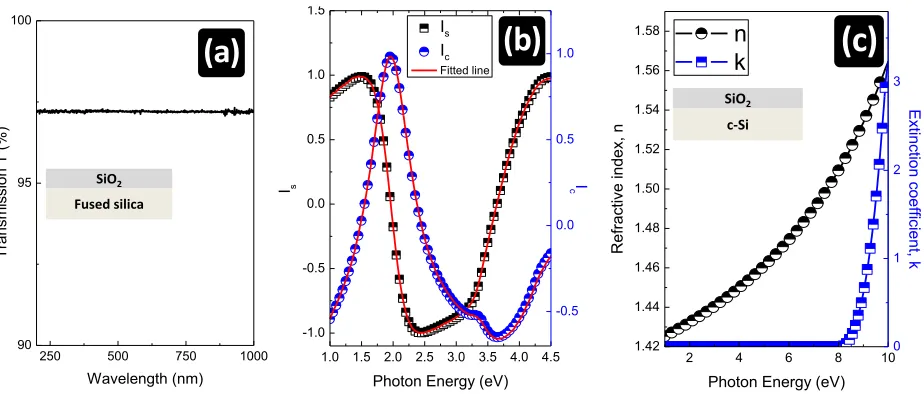
The UV-Vis transmission spectra of SiO2 films spray coated on fused silica substrates at 350 oC
are shown in Figure 1a. The spectra demonstrate films of high optical quality with an average
transmittance (%) in the visible (400 nm – 700 nm) of about 97 %. As expected though, no optical
transitions of the SiO2 films near the band edge were observed at such low photon energies. As a
result, the optical properties of SiO2 films were further investigated by ex situ UV–Visible
spectroscopic ellipsometry in the range of photon energies from 1 to 4.5 eV.
As discussed, parameterization of the dielectric functions of SiO2 (or amorphous materials in
general) in the near UV to near IR range is based on the quantum mechanical or Lorentz oscillator
and the Tauc joint density of states model initially developed by Forouhi and Bloomer25,26
McGahan and Woolam27 and modified by Jellison and Modine to address certain issues and correct
some errors and inconsistencies.28 It should be noted though that this parameterization includes
only interband transitions. Any Urbach tail absorption, intraband absorption or defect absorption, ,
or are not explicitly included in the model.
Figure 1: a) Transmittance T% in the photon range between 200 nm and 1000 nm of SiO2 sprayed
coated at 350 oC on fused silica substrates. b) Experimental data and fitted lines of the parameters IS=sin2sin and IC= sin2cos of SiO2 films sprayed at 350 oC on silicon substrates. The fitted
lines were calculated by means of a modified version of the Forouhi–Bloomer model27 and the
effective-medium approximation c) Refractive index and extinction coefficient of SiO2 films spray
coated at 350 oC as derived from spectroscopic ellipsometry.
For SiO2 films, one oscillator (only five parameters are needed, see experimental section) provides
an excellent fit to the data as shown in Figure 1b. The "extended to high energies" refractive index
(n) and extinction coefficient (k) dispersions are illustrated in Figure 1c. The optical band gap (as
derived by extrapolation) was found to be 8.11 eV consistent with the values calculated for
thermally grown SiO2 (8.13) measured under the same conditions. Additionally, the infinite
dielectric constant (ε∞) was found to be 18.5 yielding in turn a pinning factor S29 of 0.94,
comparable with the reported values for thermally grown SiO2.30
X-ray diffraction revealed amorphous films (no features of crystalline SiO2) and thus the
microstructure of the spray coated SiO2 films on KBr was further investigated by FTIR. The IR
250 500 750 1000
90 95 100
(a)
SiO2 Fused silica Tr ansm is sion T (%
)
Wavelength (nm)
1.0 1.5 2.0 2.5 3.0 3.5 4.0 4.5 -1.0 -0.5 0.0 0.5 1.0 1.5
(b)
Is Ic Fitted linePhoton Energy (eV)
Is -0.5 0.0 0.5 1.0 I c
2 4 6 8 10
1.42 1.44 1.46 1.48 1.50 1.52 1.54 1.56 1.58 SiO2 c-Si n k
Photon Energy (eV)
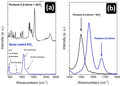
[image:9.612.77.539.124.321.2]spectra of both the precursor solution (SiCl4 in pentane-2,4-dione) as well as the SiO2 film that
was deposited at 350 oC are shown in Figure 2a. One can immediately observe the lack of any
features due to impurities or residual species (pentane-2,4-dione or SiCl4) in the SiO2 film
spectrum. Only four prominent peaks are present i.e. the Si–O out-of-plane rocking mode at 460
cm−1, the Si–O bending mode at 800 cm−1, and the Si–O and Si–O–Si stretching modes at 1080
cm−1 and 1200 cm-1 respectively.31 In addition, the FTIR spectrum of the SiO2 films reveals no
(or extremely weak) features at 3400 cm−1 or at 3650 cm−1 which would correspond to the H–O–
H and the Si–O–H stretching modes respectively. This further confirms that no OH groups were
incorporated into the SiO2 film during or after deposition. Further analysis of the FTIR spectra in
the range between 1450 cm-1 and 1850 cm-1 provides more details on the structure of the precursor
solution. Indeed, Figure 2b provides evidence of the reaction between pentane-2,4-dione and SiCl4
to yield tris-(2,4-pentanedione)-silicon chloride HCl, a compound with a decomposition
temperature in the range between 170 oC and 174 oC32. Tris-(2,4-pentanedione)-silicon chloride
1-hydrogen chloride shows no infrared absorption in the carbonyl region near 1700 cm-1, and instead
has a single very strong and broad absorption band at about 1555 cm-1. This intensity enhancement
and very large shift of the C-O absorption band can only be accounted for by assuming that the
carbonyl oxygens form strong complexes with an acidic site, which should in this case be the
silicon atom. Such absorption behavior was found in metal chelates, all of which show strong
bands in the 1500-1600 cm-1 region.32 We equally conclude that our precursor solution is a
compound whose structure has three acetylacetonate groups which are chelated about a silicon ion,
occupying six 3s3p33d2 hybrid orbitals octahedrally distributed about the silicon.
Figure 2:a) FTIR spectra in the region between 400 cm-1 and 4000 cm-1 of the precursor solution
(SiCl4 in pentane-2,4-dione) and SiO2 films deposited by spray pyrolysis on KBr substrates. The
spectra confirm complete decomposition of the precursors and further confirm SiO2 deposition.
The SiO2 shows four prominent peaks i.e. the Si–O out-of-plane rocking mode at 460 cm−1, the
Si–O bending mode at 800 cm−1, and the Si–O and Si–O–Si stretching modes at 1080 cm−1 and
1200 cm-1 respectively. b) FTIR spectra in the region between 1450 cm-1 and 1850 cm-1 of the precursor solution (SiCl4 in pentane-2,4-dione) and the pentane-2,4-dione solvent. The absence of
the infrared absorption band in the carbonyl region near 1700 cm-1, and instead the single very strong and broad absorption band at about 1555 cm-1 indicate the formation of Tris-(2,4-pentanedione)-silicon chloride HCl in the precursor solution.
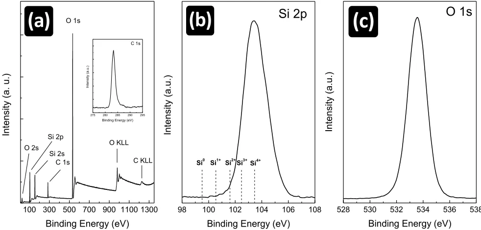
The films’ stoichiometry was further investigated by X-ray photoelectron spectroscopy so that
more information on the Si-O bonding energies and elemental composition could be obtained and
confirmed that stoichiometric SiO2 was indeed formed. The XPS spectrum of spray coated SiO2
in the energy range between 10 eV and 1350 eV is illustrated in Figure 3a.
500 1000 1500 3000 4000
(a)
Si-O-Si stretching Si-O stretching
Si-O bending Si-O out of plane deformation
Spray coated SiO2
Intensi
ty
(a. u.)
Wavenumbers (cm-1)
Pentane-2,4-dione + SiCl4
1450 1550 1650 1750 1850
Pentane-2,4-dione + SiCl4
Pentane-2,4-dione
(b)
Intensi
ty
(a. u.)
Wavenumbers (cm-1)
Figure 3:a) Wide scan XPS spectra of SiO2 films (130 nm) sprayed coated at 350 oC on silicon
substrates (inset: C 1s core level curve). High resolution b) Si 2p and c) O 1s XPS spectra. The main peaks observed were the Si 2p, Si 2s, C 1s and O 1s photoemission peaks at binding energies of 104, 150, 285 and 533 eV respectively, with O and C Auger KLL peaks at 990 eV and 1225 eV respectively. No features from any other elements contributed to the spectrum.
Further narrow region energy scans allowed determination of the chemical state of the specific
element identified as depicted in Figure 3b, and Figure 3c as Si 2p and O 1s respectively. Figure 3b clearly demonstrates that the dominant chemical structure is that of the Si4+ oxidation state that
corresponds to SiO2. Additionally, the absence of any features at 99.5 eV (Si0)33,34 further confirms
the precursor’s conversion to SiO2. Last but not least, the relative atomic concentration ratio Si:O
was calculated from the intensities of the major photoelectron spectral lines by means of codes
incorporated in the instrument data system using Scofield cross sections35 and found to be 0.5
further confirming SiO2 growth.
The surface morphologies of an ITO coated glass substrate, spray coated SiO2 on ITO coated glass
and a 400 nm reference thermal oxide were investigated by atomic force microscopy (AFM) and
100 300 500 700 900 1100 1300
(a)
275 280 285 290 295
C 1s
In
te
n
sit
y
(a
.u
.)
Binding Energy (eV)
O 2s
Si 2p
Si 2s
C 1s
O KLL
Intensi
ty
(a. u.)
Binding Energy (eV)
C KLL
98 100 102 104 106 108
Si0 Si4+
Intensi
ty
(a.u.)
Binding Energy (eV)
Si2+Si3+
Si1+
528 530 532 534 536 538
(c)
Intensi
ty
(a.u.)
Binding Energy (eV)
a high frequency (MHz) but very small amplitude (sub-nm) ultrasonic vibration applied to the
device. The oscillating strain field propagates to the subsurface of the sample equally probing the
integrity of buried structures and interfaces and provides high sensitivity nanoscale resolution
mapping of solid state materials with a wide range of elastic moduli (from 100 MPa to several
100s GPa). Moreover, the surface damage to the sample and the tip during UFM imaging is
negligible because of the effect of ultrasound-induced lubricity that eliminates the shear forces
during the scanning.38
AFM and UFM topography images of the ITO coated glass substrate, spray coated SiO2 and
thermally grown SiO2 are depicted in Figure 4. The images presented are the raw images as further
image processing (e.g. for tip dilation) was omitted as it showed no improvement of the image
quality. The films’ surface was investigated in terms of root-mean-square roughness and found to
be 1.21 nm for ITO considerably higher than those of spray coated (0.55 nm) SiO2 (on ITO)
and thermally grown (0.15 nm) SiO2. The obvious differences in films morphology indicate that
the SiO2 surface morphology and growth is dominated by the deposition process rather than the
morphology of the underlying ITO-coated glass substrate. This low surface roughness for the spray
coated SiO2 (comparable to that of thermally grown SiO2) constitutes a promising finding for the
implementation of spray coated SiO2 dielectrics into thin film transistors.
Figure 4: AFM and UFM topography images (and RRMS roughness inset) of a) commercially
available ITO, b) Thermally grown SiO2, and c) SiO2 films on ITO spray coated at 350 oC in air.
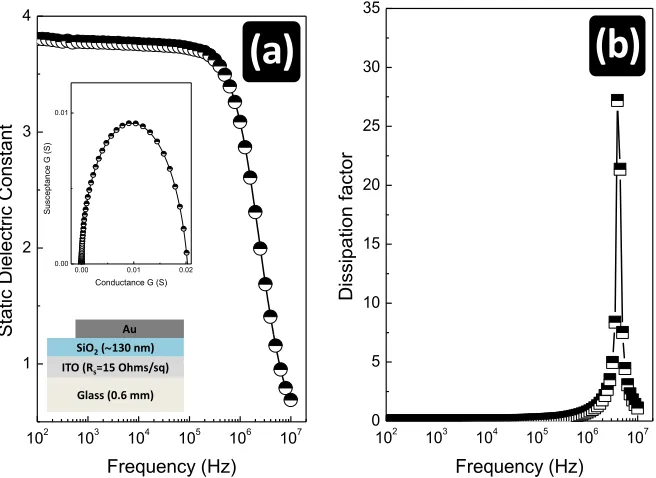
The leakage currents and dielectric properties of SiO2 films were obtained by employing a
metal-insulator-metal device architecture. Spray coated SiO2 films of thickness of ~130 nm were
sandwiched between ITO and Au electrodes (inset Figure 5a). The static dielectric constant
dispersion in the frequency range between 100 Hz and 10 MHz is shown in Figure 5a. The Nyquist
plot as well as the dissipation factor (DF), are illustrated in the inset in Figure 5a and in Figure 5b
respectively. The static dielectric constant as derived by the geometric capacitance at 100 Hz
(extracted from the Bode plot) was found to be 3.8 in very good agreement with that reported
(3.9) for SiO2. The dissipation factor (DF) was found to be as small as 0.1 at low frequencies,
[image:14.612.186.419.71.418.2]indicating excellent capacitive properties. The DF resonance at about 4 MHz is attributed to dipole
relaxation. In addition, the Nyquist plot (inset Figure 5a) reveals a stable system whose equivalent
circuit consists of a capacitor with high shunt and low series resistance.
Figure 5: a) Dielectric constant dispersion in the frequency range between 100 Hz and 10 MHz (inset, Nyquist plot and MIM device architecture) and b) Dissipation factor of SiO2 films at 350 oC in air.
The current density versus electric field characteristics of the same MIM device (ITO/SiO2
(130 nm)/Au(100 nm)) are shown in Figure 6a. As shown, the devices exhibit excellent
dielectric strength and no dielectric breakdown was observed for electric fields as high as 5
MV cm-1. In an effort to determine the leakage current mechanism, Figures 6b and 6c show
the Fowler Nordheim (N) and Poole-Frenkel (P-F) plots of the same characteristics. Both
F-N and P-F plots shows some linearity at high electric field indicating that the conduction could
equally be determined by either F–N tunneling (i.e. an interface limited process) or P-F i.e.
bulk-limited. Based on the data illustrated in Figure 6, and given the linearity over a limited 102 103 104 105 106 107
1 2 3 4
(a)
ITO (Rs=15 Ohms/sq)
Glass (0.6 mm)
SiO2(130 nm)
Au
0.00 0.01 0.02
0.00 0.01
S
us
ceptan
ce G (
S
)
Conductance G (S)
S
tati
c Di
el
ec
tri
c Constant
Frequency (Hz)
102
103
104
105
106
107
0 5 10 15 20 25 30 35
(b)
Di
ss
ipati
on factor
Frequency (Hz)
[image:15.612.127.455.160.399.2]electric field range for both plots, we can’t safely decide upon the dominant conduction
mechanism. Figure 2c, certainly infers the presence of trap states and barrier height lowering
at high electric fields however the origin of such trap states, previously associated with
nano-porous SiO2 films deposited by sol-gel39, remains unknown and such a hypothesis is not
supported by UFM measurements (Figure 4c) that show porous-free films. A F-N dependence
has been observed for thermally grown SiO2,40 and a Poole-Frenkel type (i.e. bulk limited) of
conduction has also been reported for SiO2 that was deposited from solutions and treated with
plasma.41 Further measurements on the temperature dependence of the plots would help to
clarify the situation, however such detailed investigation is outside the scope of the present
study.
Figure 6: a) Leakage current density b) Fowler-Nordheim plot (inset: extended Fowler-Nordheim plot) and c) Poole-Frenkel plot (inset: extended Poole-Frenkel plot) of a 130 nm SiO2 MIM
device deposited by spray pyrolysis at 350 oC.
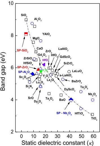
Finally, Figure 7depicts the band gap and static dielectric constant of a wide range of dielectric
materials (including the findings of the present study) grown by a wide range of deposition
-1 0 1 2 3 4 5
10-9 10-8 10-7 10-6 10-5 10-4
(a)
ITO (Rs=15 Ohms/sq)
Glass (0.6 mm) SiO2(130 nm)
Au Curr ent den si ty , J ( A /c m 2 ) E (MV/cm)
0.20 0.25 0.30 0.35 0.40 10-20 10-19 10-18 10-17
F-N
(b)
0.1 1 10 100
10-20 10-19 10-18 10-17 10-16 J E
-2 (
A
V
-2)
1/E (cm MV-1
)
J E
-2 (
A
V
-2 )
1/E (cm MV-1)
1.25 1.50 1.75 2.00 2.25
10-14 10-13 10-12 10-11 10-10
0.0 0.5 1.0 1.5 2.0 2.5 10-14 10-13 10-12 10-11 J E
-1 (
A
V
-1)
E1/2 (MV/cm)1/2
(c)
J E
-1 (
A
V
-1 )
E1/2 (MV/cm)1/2
[image:16.612.77.525.357.560.2]techniques, including solution processed ones, further demonstrating the well-established
[image:17.612.218.395.135.391.2]dielectric constant-band gap trend of both vacuum42,43 and solution processed gate dielectrics.21
Figure 7: Static dielectric constant vs band gap for oxide gate dielectric grown by a wide range deposition methods both vacuum and solutions based.
The performance of spray coated SiO2 films as a gate dielectric was investigated in a bottom-gate,
top-contact (BG–TC) TFT architecture (inset, Figure 8 and 9) employing C60 and pentacene as
channel semiconductors. The organic layers as well as the source and drain contacts were
evaporated under high vacuum conditions as described in the experimental section. The devices
were measured under vacuum immediately after deposition.
0 10 20 30 40 50 60
2 4 6 8 10
SP - Nb2O5 SP-SiO2
Gd2O3
Sc2O3
Dy2O3
YAlO3
BaZrO3
Ta2O5
HfTiO4
Nb2O5 DyScO3
SrZrO4 GdScO3 LaAlO3
Lu2O3
LaLuO3
a-LaAlO3 HfO2
SP-Al2O3
Y2O3
SP-ZrO2
La2O3
Si3N4
Y2O3
SrO Ta2O5
TiO2
BaO HfO2
ZrO2
HfSiO4
B
and ga
p (eV
)
Static dielectric constant ()
SiO2 Al2O3
MgO
CaO
ZrSiO4 3
Figure 8: Linear (VDS = 2 V) and saturated (VDS = 25 V) transfer characteristics of bottom-gate,
top-contact (inset: architecture employed) TFTs with channel width W= 1000 µm and channel length L = 10 µm, employing an evaporated C60 semiconducting channel on a 26 nF/cm2 spray
coated SiO2 dielectric.
Figures 8 and 9 show a representative set of transfer characteristics obtained from C60 and
pentacene TFTs (L = 10 μm, W = 1000 μm) based on a ~130 nm (Cox 26 nF/cm2) thick SiO2
dielectric. The devices exhibit excellent operating characteristics with low voltage operation,
negligible hysteresis, high on/off current modulation ratio in the order of 106 and high carrier
mobility of approximately 0.6 cm2 V-1 s-1 and 0.02 cm2 V-1 s-1 for C
60 and pentacene TFT
respectively.
-10 -5 0 5 10 15 20 25
10-10
10-9
10-8
10-7
10-6
10-5
10-4
10-3
VGS (V)
I DS
(A
)
0 5 10 15 20 25
ITO (Rs=15 Ohms/sq)
Glass (0.6 mm) SiO2(130 nm)
C60(40 nm)
Ca/Al Ca/Al
L= 10 m
W= 1000 m
(I
DS
,SAT
) 1/2
(mA
1/2
)
VD= 2, 25 V
= 0.6 (cm2
/Vs)
Vth= 5 V
Figure 9: Linear (VDS = -2 V) and saturated (VDS = -30 V) transfer characteristics of bottom-gate,
top-contact (inset: architecture employed) TFTs with channel width W= 1000 µm and channel length L = 10 µm, employing a pentacene semiconducting channel on a 26 nF/cm2 spray coated SiO2 dielectric.
4. CONCLUSION
We have demonstrated the production of solution processed SiO2 dielectrics over large areas under
ambient conditions at moderate substrate temperatures of 350 oC and their implementation in
(both electron and hole transporting) TFTs employing organic semiconducting channels. The films
were spray coated from silicon chloride blends in pentane-2,4-dione and the films’ physical
properties were investigated by a wide range of characterization techniques that demonstrated the
production of ultra-smooth amorphous SiO2 films, with wide band gap, dielectric constant similar
to that of thermally grown SiO2 and similar leakage currents. The TFTs that were manufactured
using SiO2 layers as gate dielectrics showed excellent characteristics in terms of carrier mobilities
(both electrons and holes), negligible hysteresis, and high on/off current ratios.
Finally, the excellent reproducibility and films’ homogeneity, combined with the relatively low
-for SiO2- deposition temperature in ambient air on substrates other than silicon, indicates the
-30 -25 -20 -15 -10 -5 0 5 10-12
10-11
10-10
10-9
10-8
10-7
10-6
10-5
10-4
VGS (V)
-I DS
(A
)
0 1 2 3 4
ITO (Rs=15 Ohms/sq)
Glass (0.6 mm) SiO2(130 nm)
Pentacene (40 nm)
Au Au
L= 10 m W= 1000 m
(I
DS
,
SAT
) 1
/2
(mA
1
/2
)
VD= -2, -30 V
= 0.02 (cm2/Vs)
Vth= -14.5 V
potential for the rapid development of organic TFTs on SiO2 gate dielectrics grown from solutions
at low manufacturing cost.
AUTHOR INFORMATION
Corresponding Author
*Dr George Adamopoulos. Email: [email protected]
Notes
The authors declare no competing financial interest.
ACKNOWLEDGMENTS
M.E. is grateful for support from the Ministry of Education Malaysia and Faculty of Electronics
and Computer Engineering, Universiti Teknikal Malaysia Melaka (UteM).
REFERENCES
(1) Green, M. L.; Gusev, E. P.; Degraeve, R.; Garfunkel, E. L. Ultrathin (<4 Nm) SiO2 and
Si-O-N Gate Dielectric Layers for Silicon Microelectronics: Understanding the Processing, Structure, and Physical and Electrical Limits. J. Appl. Phys.2001, 90 (5), 2057–2121. (2) Helms, C. R.; Poindexter, E. H. The Silicon-Silicon-Dioxide System : Its Microstructure
and Imperfections. Rep. Prog. Phys.1994, 57, 791–852.
(3) Gusev, E. P.; Lu, H.-C.; Garfunkel, E. L.; Gustafsson, T.; Green, M. L. Growth and Characterization of Ultrathin Nitrided Silicon Oxide Films. IBM J. Res. Dev.1999, 43, 265– 286.
(4) Klaus, J. W.; Sneh, O.; George, S. M. Growth of SiO2 at Room Temperature with the Use
of Catalyzed Sequential Half-Reactions. Science1997, 278, 1934–1936.
(5) Watanabe, K.; Tanigaki, T.; Wakayama, S. The Properties of LPCVD SiO2 Film Deposited
by SiH2Cl2 and N2O Mixtures. J. Electrochem. Soc.1981, 128, 2630–2635.
(6) Kern, W.; Rosler, R. S. Advances in Deposition Processes for Passivation Films. J. Vac.
Sci. Technol.1977, 14, 1082-1099.
(7) Becker, F. S.; Pawlik, D.; Anzinger, H.; Spitzer, A. Low‐pressure Deposition of High‐ quality SiO2 Films by Pyrolysis of Tetraethylorthosilicate. J. Vac. Sci. Technol. B 1987, 5,
1555-1563.
(8) Hamelmann, F.; Heinzmann, U.; Szekeres, A.; Kirov, N.; Nikolova, T. Deposition of Silicon Oxide Thin Films in TEOS with Addition of Oxygen to the Plasma Ambient: IR Spectra Analysis. J. Optoelectron. Adv. Mater.2005, 7, 389–392.
(9) Kim, J.; Hwang, S.; Yi, J. SiO2 Films Deposited at Low Temperature by Using APCVD
with TEOS/O3 for TFT Applications. J. Korean Phys. Soc.2006, 49, 1121–1125.
(10) Rha, S.; Chou, T. P.; Cao, G.; Lee, Y.; Lee, W. Characteristics of Silicon Oxide Thin Films Prepared by Sol Electrophoretic Deposition Method Using Tetraethylorthosilicate as the Precursor. Curr. Appl. Phys.2009, 9, 551–555.
(11) Rashid, R.; Flewitt, A. J.; Grambole, D.; Kreiβig, U.; Robertson, J.; Milne, W. I. High Quality Growth of SiO2 at 80° C by Electron Cyclotron Resonance (ECR) for Thin Film
Transistors. MRS Online Proc. Libr.2001, 685, D13.1.1.
(12) Hamakawa, M. O. and Toyoda, Y. Photo-Induced Chemical Vapor Deposition of SiO2 Film
Using Direct Excitation Process by Deuterium Lamp. Jpn. J. Appl. Phys. 1984, 23, L97-L99.
(13) Masakiyo Matsumura, S. M. and Y. U. and. Atomic-Layer Chemical-Vapor-Deposition of SiO2 by Cyclic Exposures of CH3OSi(NCO)3 and H2O2. Jpn. J. Appl. Phys.1995, 34,
5738-5742.
(14) Tripp, C. P.; Hair, M. L. Chemical Attachment of Chlorosilanes to Silica: A Two-Step Amine-Promoted Reaction. J. Phys. Chem.1993, 97, 5693–5698.
(15) Blitz, J. P.; Murthy, R. S. S.; Leyden, D. E. Ammonia-Catalyzed Silylation Reactions of Cab-O-Sol with Methoxymethylsilanes. J. Am. Chem. Soc.1987, 109, 7141–7145.
(16) Dingemans, G.; Helvoirt, C. A. A. Van; Pierreux, D.; Keuning, W.; Kessels, W. M. M. Plasma-Assisted ALD for the Conformal Deposition of SiO2 : Process , Material and
Electronic Properties. J. Electrochem. Soc.2012, 159 (3), H277–H285.
(17) Burton, B.; Boleslawski, M. Rapid SiO2 Atomic Layer Deposition Using Tris
(Tert-Pentoxy) Silanol. Chem. Mater.2008, 20, 7031–7043.
(18) Burton, B. B.; Kang, S. W.; Rhee, S. W.; George, S. M. SiO2 Atomic Layer Deposition
Using Tris (Dimethylamino) Silane and Hydrogen Peroxide Studied by in Situ Transmission FTIR Spectroscopy. J. Phys. Chem. C.2009, 113, 8249–8257.
(19) Jeong, Y.; Pearson, C.; Kim, H.; Park, M.; Kim, H.; Do, L.; Petty, M. C. Optimization of a Solution-Processed SiO2 Gate Insulator by Plasma Treatment for Zinc Oxide Thin Film
Transistors. ACS Appl. Mater. Interfaces2016, 8, 2061–2070.
(20) Jeong, Y.; Pearson, C.; Kim, H.-G.; Park, M.-Y.; Kim, H.; Do, L.-M.; Petty, M. C. Solution-Processed SiO2 Gate Insulator Formed at Low Temperature for Zinc Oxide Thin-Film
Transistors. RSC Adv.2015, 5, 36083–36087.
(21) Esro, M.; Vourlias, G.; Somerton, C.; Milne, W. I.; Adamopoulos, G. High-Mobility ZnO Thin Film Transistors Based on Solution-Processed Hafnium Oxide Gate Dielectrics. Adv. Funct. Mater.2015, 25, 134–141.
(22) Adamopoulos, G.; Thomas, S.; Bradley, D. D. C.; McLachlan, M. A.; Anthopoulos, T. D. Low-Voltage ZnO Thin-Film Transistors Based on Y2O3 and Al2O3 High-K Dielectrics
Deposited by Spray Pyrolysis in Air. Appl. Phys. Lett.2011, 98,123503-1 - 123503-3. (23) Adamopoulos, G.; Thomas, S.; Wöbkenberg, P. H.; Bradley, D. D. C.; McLachlan, M. A.;
Anthopoulos, T. D. High-Mobility Low-Voltage ZnO and Li-Doped ZnO Transistors Based on ZrO2 High-K Dielectric Grown by Spray Pyrolysis in Ambient Air. Adv. Mater. 2011,
23, 1894–1898.
(24) Afouxenidis, D.; Mazzocco, R.; Vourlias, G.; Livesley, P. J.; Krier, A.; Milne, W. I.; Kolosov, O.; Adamopoulos, G. ZnO-Based Thin Film Transistors Employing Aluminum Titanate Gate Dielectrics Deposited by Spray Pyrolysis at Ambient Air. ACS Appl. Mater. Interfaces2015, 7, 7334–7341.
(25) Forouhi, A. R.; Bloomer, I. Optical Dispersion Relations for Amorphous Semiconductors and Amorphous Dielectrics. Phys. Rev. B1986, 34, 7018–7026.
(26) Forouhi, A. R.; Bloomer, I. Optical Properties of Crystalline Semiconductors and Dielectrics. Phys. Rev. B1988, 38, 1865–1874.
(27) McGahan, W. A.; Makovicka, T.; Hale, J.; Woollam, J. A. Modified Forouhi and Bloomer Dispersion Model for the Optical Constants of Amorphous Hydrogenated Carbon Thin Films. Thin Solid Films.1994, 253, 57–61.
(28) Jellison, G. E.; Modine, F. A. Parameterization of the Optical Functions of Amorphous Materials in the Interband Region. Appl. Phys. Lett.1996, 69, 371-373.
(29) Mönch, W. Role of Virtual Gap States and Defects in Metal-Semiconductor Contacts. Phys. Rev. Lett.1987, 58, 1260–1263.
(30) Robertson, J. Band Offsets of Wide-Band-Gap Oxides and Implications for Future Electronic Devices. J. Vac. Sci. Technol. B2000, 18 (3), 1785-1791.
(31) Zacharias, M.; Dlmova-malinovska, D.; Stutzmann, M. Properties of Hydrogenated Amorphous Silicon Suboxide Alloys with Visible Room-Temperature Photoluminescence.
Philos. Mag. Part B1996, 73 (5), 799–816.
(32) West, R. Silicon and Organosilicon Derivatives of Acetylacetone. J. Am. Chem. Soc., 1958, 80 (13), pp 3246–3249.
(33) Kim, S.; Kim, M. C.; Choi, S.; Kim, K. J.; Hwang, H. N.; Hwang, C. C.; Kim, S.; Kim, M. C.; Choi, S. Size Dependence of Si 2P Core-Level Shift at Si Nanocrystal/SiO Interfaces.
Appl. Phys. Lett. 2007, 91, 103113-1 - 103113-3.
(34) Kim, K. J.; Kim, J. W.; Yang, M. S.; Shin, J. H. Oxidation of Si during the Growth of SiOx by Ion-Beam Sputter Deposition: In Situ X-Ray Photoelectron Spectroscopy as a Function of Oxygen Partial Pressure and Deposition Temperature. Phys. Rev. B - Condens. Matter Mater. Phys.2006, 74 (15), 2–5.
(35) Saloman, E. B.; Hubbell, J. H.; Scofield, J. H. X-Ray Attenuation Cross Sections for Energies 100 eV to 100 keV and Elements Z = 1 to Z = 92 At. Data Nucl. Data Tables1988,
38, 1–196.
(36) Dinelli, F.; Assender, H. E.; Takeda, N.; Briggs, G. A. D.; Kolosov, O. V. Elastic Mapping of Heterogeneous Nanostructures with Ultrasonic Force Microscopy (UFM). Surf. Interface Anal.1999, 27, 562–567.
(37) Bosse, J. L.; Tovee, P. D.; Huey, B. D.; Kolosov, O. V. Physical Mechanisms of Megahertz Vibrations and Nonlinear Detection in Ultrasonic Force and Related Microscopies. J. Appl. Phys. Lett 2014, 115, 144304-1 - 144304-7.
(38) Dinelli, F.; Biswas, S. K.; Briggs, G. A. D.; Kolosov, O. V. Ultrasound Induced Lubricity in Microscopic Contact. Appl. Phys. Lett.1997, 71, 1177-1179.
(39) Jaehnike, F.; Pham, D.; Anselmann, R.; Bock, C.; Kunze, U. High-Quality Solution-Processed Silicon Oxide Gate Dielectric Applied on Indium Oxide Based Thin-Film Transistors. ACS Appl. Mater. Interfaces,2015, 7 (25), pp 14011–14017.
(40) Lenzlinger, M.; Snow, E. H. Fowler ‐ Nordheim Tunneling into Thermally Grown SiO2. J.
Appl. Phys. 1969, 40, 278-283.
(41) Jeong, Y.; Pearson, C.; Kim, H.; Park, M.; Kim, H.; Do, L.; Petty, M. C. Optimization of a Solution-Processed SiO2 Gate Insulator by Plasma Treatment for Zinc Oxide Thin Film
Transistors. ACS Appl. Mater. Interfaces, 2016, 8, 2061–2070.
(42) Robertson, J.; Wallace, R. M. High-K Materials and Metal Gates for CMOS Applications.
Mater. Sci. Eng., R.2015, 88, 1–41.
(43) Robertson, J. High Dielectric Constant Gate Oxides for Metal Oxide Si Transistors. Rep. Prog. Phys.2005, 69, 327–396.
TOC Figure: