Microstructure of Erbium Oxide Thin Film on SUS316 Substrate with Y
2O
3or
CeO
2Buffer Layers Formed by MOCVD Method
Seungwon Lee
1, Takayuki Shinkawa
2,*1, Kenji Matsuda
1,*2, Masaki Tanaka
3, Yoshimitsu Hishinuma
3,
Katsuhiko Nishimura
1, Teruya Tanaka
3, Takeo Muroga
3and Takahiro Sato
4 1Graduate School of Science and Engineering for Research, University of Toyama, Toyama 930–8555, Japan 2Graduate School of Science and Engineering for Education, University of Toyama, Toyama 930–8555, Japan 3National Institute of Fusion Science, Toki, 509–5292, Japan4Hitachi High-Technologies Corp., Hitachinaka, 312–0057, Japan
Er2O3 has been known the best candidate material for insulating coating for liquid metal breeding blanket system. The formation of Er2O3 layer by MOCVD method can be succeeded on SUS316 substrate with CeO2 and Y2O3 buffer layers (100 nm and 500 nm) fabricated by RF sputtering, and their microstructures have been confirmed by SEM, TEM and STEM. The surface morphology of their layers was smaller gran-ular structure than the previous study without buffer layer. According to cross sectional TEM (X-TEM) observation, Er2O3, CeO2/Y2O3 buffer, unknown layers and SUS substrate can be confirmed. CeO2 buffer layer has a granular structure, while Y2O3 has a columnar structure. Er2O3 layer formed on each buffer layer had finer structure without buffer layer. It has been also detected that each element does not exist so much in each layer by diffusion during fabrication according to STEM-EDS and HAADF imaging. [doi:10.2320/matertrans.M2016313]
(Received September 5, 2016; Accepted November 28, 2016; Published January 16, 2017)
Keywords: erbium oxide, buffer layers, metal organic chemical vapor deposition (MOCVD), microstructure, transmission electron microsco-py
1. Introduction
Er2O3 has been focused on a material as an insulating coat-ing for a liquid lithium blanket.1) In the practical usage point of view, hydrogen permeation test for the advanced breeding blanket system is important using the ideal samples which have coated surface by Er2O3. Hishinuma et. al. succeeded to form Er2O3 film on SUS316 by MO-CVD method by their original way, and it shows lower roughness of film surface and nice property for scratch test,2) and its film has been in-vestigated in our previous report.3)
In order to enhance the performance of Er2O3 coating as an electrical insulator and e hydrogen permeation burrier, it is necessary to form thicker coating is higher crystallinity. How-ever, the epitaxial growth like a chemical vapor deposition is difficult to form thicker coating layer on a metal substrate. For the thicker oxide coating formation, generally, it is effec-tive to stack simply oxide coating into layer by layer. Further-more, the crystallinity of oxide coating layer is improved by the matching of the lattice constant between the oxide layer and the buffer layer. There is a report for YBa2Cu3O7 (YBCO) superconductor which has buffer layers of CeO2 and Y2O3, and YBCO crystalline grow epitaxy on those layers.4)
In our recent study, yttrium oxide and cerium oxide, having the similar lattice constant to that of erbium oxide crystalline and a substrate material, and the effect of buffer layer forma-tion on the nano-structure and the hydrogen permeaforma-tion prop-erty of double stacked coating layer was investigated, and its possibility to form these buffer layers on the SUS substrate. Er2O3 and Y2O3 and CeO2 crystalline have the cubic struc-ture, and Er2O3 and Y2O3 are C-rare earth structure, and CeO2
is CaF2 structure. The lattice parameters of Er2O3 and Y2O3 are 1.06 nm, almost similar to each other, and the lattice pa-rameter of CeO2 is the half of 1.06 nm.5)
In this study, microstructures and the relationship between Er2O3 layer and buffer-layers of Y2O3 or CeO2 formed by RF-sputtering method on a substrate has been investigated using transmission electron microscopy (TEM) for the cross sectioned TEM samples prepared by the focused ion beam technique to investigate crystallinity and the morphology of their crystalline.
2. Experimental Procedure
The buffer-layers of Y2O3 or CeO2 has been formed by RF-sputtering method on a commercial SUS 316 disc plate, and then the Er2O3 film has formed by a metal organic chem-ical vapor deposition (MOCVD) method. The buffer layers of Y2O3 and CeO2 were fabricated by the conventional RF sput-tering method. The condition of MOCVD was the same as the previous report3) using metal organic material of Er(IBPM)
3 and the substrate temperature was 500 C. The mention of thickness of Er2O3 was about 150 nm. The roughness of Er2O3 was about 25 nm. After MOCVD, sample discs took out from the machine, and provided for analysis of micro-structure or the hydrogen permeation test. Scanning, trans-mission, and scanning-transmission electron microscopes (SEM (Hitachi S3500), TEM (Topcon EM-002B), STEM (Hitachi HD7200)) were used for analysis of microstructure in samples.
Small tips of cross sectional TEM (X-TEM) samples for TEM observation were prepared perpendicular to the sample surface and parallel to gas flow on MOCVD by FIB method. FIB was Hitachi FB-2100. The dimension of small tip of X-TEM sample was about 12 μm × 2 μm, and its thickness is less than 100 nm. The accelerating voltage of FIB was 40 kV
*1
Graduate Student, University of Toyama. Present address: Ahresty Corp., Toyohashi 441–3153, Japan
*2
for Ga+ ion, and the aperture size was 520 μm in the first for rough milling, and then changed to the smallest aperture size of 15 μm for final milling, gently.
3. Results and Discussion
3.1 100 nm CeO2
Figure 1 show overviews and SEM images of sample with Er2O3/100 nm CeO2 –buffer/SUS, Er2O3/100 nm Y2O3 – buffer/SUS, Er2O3/500 nm CeO2 –buffer/SUS, and Er2O3/500 nm Y2O3 –buffer/SUS substrates. A rainbow col-or depending on the difference of thickness by oxide can be seen on the surface of each sample in Fig. 1(a), (c), (e) and (g). White arrows indicate a direction of gas flow on MOCVD process. Figure 1(b), (d), (f) and (h) show SEM image of their surfaces. No remarkable particles can not observed on those surfaces, while small particles have confirmed on the surface in our previous sample without CeO2 buffer.3)
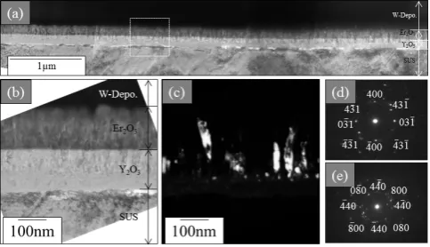
Figure 2 shows TEM images obtained for the X-TEM sam-ple of Er2O3/100 nm CeO2 –buffer/SUS substrate. Fig-ure 2(a) shows a whole area of this sample, and 5 layers can be seen in this picture. An enlarged picture in (a) marked by a white broken square is shown in Fig. 2 (b). These are tungsten deposition, Er2O3 layer, CeO2-buffer, white unknown layer and a SUS substrate. The columnar structure can be con-firmed in Er2O3 layer, while small grains can be seen in CeO2-buffer layer. The width of Er2O3 column and size of
CeO2 were 74 nm and 33 nm. The roughness of the interface between Er2O3 and CeO2, and of SUS substrate were 33 nm and 30 nm, respectively. A white layer also can be seen be-tween CeO2-buffer layer and a SUS substrate. It will be some oxide layer on a substrate according to our previous report.3) A columnar structure is visible on a dark field image of Fig. 2(c) which has been obtained for an area marked by a white square in Fig. 2(b). The selected area electron diffrac-tion (SAED) patterns were obtained from the regions of Er2O3 and CeO2 buffer layers as shown in Fig. 2(d) and (e), and these incident electron beam directions were indexed as
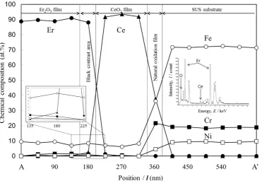
<121>Er2O3 and <121>CeO2. The chemical analysis has been performed by TEM-EDS for the interface marked by a line of A-A in Fig. 2(b). The oxygen has been omitted in this analy-sis because of difficulty for quantitative analyanaly-sis. In Fig. 3, Er is definitely the highest at the left on side of Er2O3 layer and Ce is the highest at the middle region of CeO2-buffer layer. Fe is predominant at the right on side of SUS 316 substrate, which shows 9–10 mass%Ni and 18–19 mass%Cr close to the standard SUS 316 steel. An inserted figure of the left on side is the position from 135–225 nm, and this shows inter-esting behavior of Ce, which increased at the boundary inside Er2O3 layer. It is suggested that Ce diffused from a buffer into the Er2O3 layers during MOCVD process, because of the sim-ilarity of crystal structure between CeO2 and Er2O3. The ox-ide layer around 360 nm of the position, which can be seen a white layer in Fig. 2(a), indicates higher intensity of Fe, Cr and Ni rather than those in the buffer layer. The inserted EDS profile has been obtained for the mid-point of unknown layer, and it includes oxygen as the same as the previous report.3) This unknownlayer is probably a natural Cr oxide (Cr2O3) on the SUS substrate.
Figure 4 shows images obtained by FE-STEM for the same sample of Fig. 2. Figure 4(b) and (c) are enlarged pictures marked by a black square in Fig. 4(a). The CeO2-buffer con-sists of small crystalline, and Er2O3 layer has columnar struc-ture like as the dendrite in HAADF-STEM image of Fig. 4(c). As there are no any chill crystalline or special gap between Er2O3 and CeO2 buffer, it suggested that Er2O3 grows from the CeO2 buffer by MOCVD method continuously, but its morphology is not uniform because of depending on gas flow. A thin layer between SUS substrate and CeO2 buffer can be seen as black or white color. It is provably an oxide layer. Figure 5 shows STEM-EDS maps obtained for an area marked by a white square in Fig. 4(a). Er, Ce, O and Fe show homogeneous distribution of these elements in each layer. It is noted that Cr-rich layer in Fig. 5(f) corresponds to the black layer in BF-STEM image of Fig. 5(a), and thin Fe layer in Fig. 5(e) can be seen. Small amount of Cr was detected from the CeO2 buffer layer. This means that Cr oxide layer exists on the SUS substrate and CeO2 buffer avoids the diffusion of Cr into the Er2O3. Thin Fe layer above SUS substrate in Fig. 5(e) was thinner than that in our previous report what did not have CeO2 buffer layer. It is suggested that CeO2-buffer also avoids the diffusion of Fe from the SUS substrate during the processing of MOCVD.
3.2 Effect of Thickness of buffer layer
Figure 6 shows TEM images obtained for X-TEM of Er2O3/500 nm CeO2 buffer/SUS substrate. 500 nm CeO2 Fig. 1 Overviews and SEM images of samples. (a), (b) Er2O3/100 nm
CeO2 –buffer/SUS, (c), (d) Er2O3/100 nm Y2O3 –buffer/SUS substrates, (e), (f) Er2O3/500 nm CeO2 –buffer/SUS, and (g), (h) Er2O3/500 nm Y2O3 –buffer/SUS substrates. (a), (c), (e), (g) their outlooks, and (b), (d), (f), (h) SEM images of samples.
buffer can be seen between Er2O3 and SUS substrate. The column of Er2O3 becomes wider than the sample which has the 100 nm CeO2 buffer of Fig. 2(a). The surface flatness of Er2O3 layer also became smooth. The morphology of CeO2 was an elongated grain rather than 100 nm CeO2. The SAED patterns were obtained from the regions of Er2O3 and CeO2 buffer layers as shown in Fig. 6(c) and (d), and these incident electron beam directions were indexed as <110>Er2O3 and <321>CeO2. The width of Er2O3 column and size of CeO2 were 130 nm and 104 nm. The roughness of the interface be-tween Er2O3 and CeO2, and of SUS substrate were 25 nm and 25 nm, respectively. The thick 500 nm CeO2 buffer causes worth thermal conductivity, and it introduce slow growth of Er2O3 columnar direction, then the width of Er2O3 column became wider than a sample without buffer.
Fig. 3 EDS profiles for Er, Ce, Fe, Cr and Ni elements for line A-A in Fig. 2 (b). The inserted EDS profile has been obtained for the mid-point of unknown layer.
Fig. 4 STEM images obtained for the X-TEM sample of Er2O3/100 nm CeO2 –buffer/SUS substrate in Fig. 2. (a) a BF-STEM image of whole area of this sample, (b) and (c) an enlarged BF-STEM and a HAADF images in (a) marked by a black square.
Fig. 5 (a) BF-STEM image and EDS maps of (b) Er, (c) Ce, (d) O, (e) Fe, (f) Cr obtained for the BF-STEM sample of Fig. 2 (a) marked by a white square.
[image:3.595.115.487.69.325.2] [image:3.595.308.549.380.516.2] [image:3.595.49.291.381.537.2] [image:3.595.50.291.608.735.2]3.3 buffer of Y2O3
Figure 7 shows TEM images obtained for X-TEM of Er2O3/100 nm Y2O3 buffer/SUS substrate. Figure 7(a) shows a whole area of this sample, and 4 layers can be also seen in this picture. These are tungsten deposition, Er2O3 layer, Y2O3-buffer, and a SUS substrate. The white unknown layer could not be confirmed in this case. The columnar structure can be confirmed in Er2O3 and Y2O3 buffer layers, while small grains can be seen in CeO2-buffer layer. According to the analysis of SAED patterns of Fig. 7(d) and (e), <013>Er2O3 and <001>Y2O3 were indexed. The width of Er2O3 column and Y2O3 were 60 nm and 17 nm. The roughness of the inter-face between Er2O3 and Y2O3, and of SUS substrate were 12 nm and 21 nm, respectively.
Figure 8 TEM images obtained for X-TEM of Er2O3/500 nm Y2O3 buffer/SUS substrate. The columnar structure of Y2O3 buffer and Er2O3 can be seen remarkably. The SAED patterns were obtained from the regions of Er2O3 and Y2O3 buffer layers as shown in Fig. 8(c) and (d), and these incident electron beam directions were indexed as
<001>Er2O3 and <031>Y2O3. As Er2O3 and Y2O3 have the same crystal structure of C-rare earth structure, this is an equivalent relationship with Fig. 7(d) and (e). The width of Er2O3 column and Y2O3 were 120 nm and 60 nm. The
rough-ness of the interface between Er2O3 and Y2O3, and of SUS substrate were 20 nm and 17 nm, respectively.
In our recent report for the single layer of Er2O3 on the SUS substrate3), crystalline of Er
2O3 were nucleated at some sites on the substrate surface, for example natural oxide layer, those nucleus preferentially grow from those nucleation site, and then coarse crystalline were formed on the substrate. The column width of Er2O3 on SUS substrate was 260 nm. On the other hand, if there is a buffer layer of CeO2 between Er2O3 and SUS substrate, the nucleation of Er2O3 depends on the roughness of 25–30 nm for CeO2. The column width of Er2O3 on CeO2/SUS was 70 or 130 nm for the thickness of 100 or 500 nm of CeO2, and that column width was 1/3 or a half of Er2O3 on SUS without buffer. A buffer layer of Y2O3 was also shown the similar behavior to the CeO2 layer. The roughness of Y2O3 was 12–20 nm, and the column width of Er2O3 on Y2O3/SUS was 60 or 120 nm for the thickness of 100 or 500 nm of Y2O3. This result has suggested that the surface roughness is important factor to nucleate and control the col-umn thickness of Er2O3.
The column width of columnar shaped Y2O3 was 17 or 60 nm, and it is smaller than 33 or 104 nm of granular shaped CeO2, even thickness is different from 100 to 500 nm. As Er2O3 nucleates and grows on or at those crystalline of CeO2 or Y2O3, the column width of Er2O3 is controlled by the size of crystalline of buffer layers. In this study, the crystallo-graphic orientation relationship can not be confirmed be-tween CeO2 and Er2O3, or Y2O3 and Er2O3. As Y2O3 and Er2O3 have the same crystal structure and similar lattice pa-rameter of 1.0602 nm and 1.0548 nm to each other.6) Its mis-fit was calculated by the previous work[5], and those were about 0.51% between {001}Y2O3 and {001}Er2O3 of the cube-cube relationship. Y2O3 and Er2O3, however, has been shown <001> and <031> orientation relationship in Figs. 7 and 8. This is rotating relationship about 18 degrees to each other, its misfit is calculated using other eq. (1) as follows;
mis f it(hkl)Er2O3(hkl)Y2O3[%]= d(hkl)Er2O3−d(hkl)Y2O3
d(hkl)Er2O3 ×100 (1)
The lattice misfit was calculated as 9.7% between
{007}Er2O3 and {71¯3 }Y2O3, or 5.2% between {007}Er2O3 and {226}Y2O3. As these misfit values are not small, the growth of Er2O3 on Y2O3 probably depends on the similarity of crystal structure. The orientation relationship between Er2O3 and Y2O3 or CeO2 probably depends on the condition during MOCVD process, although the column width of Er2O3 is controlled by crystalline size on the surface of Y2O3 or CeO2 buffer according to the present result.
4. Conclusions
(1) CeO2 or Y2O3 buffer layer of 100 or 500 nm in thickness has been prepared on the SUS 316 substrate by RF-sput-tering method, and the Er2O3 layer could be formed on CeO2 or Y2O3buffer layers about 150–280 nm.
(2) The surface roughness of Er2O3/CeO2/SUS and Er2O3/ Y2O3/SUS were 25–30 nm and 12–20 nm respectively, while it was 140 nm without buffer.
(3) CeO2 with granular structure has been formed on SUS substrate, and it makes smaller columns of Er2O3 than the Fig. 7 TEM images obtained for the X-TEM sample of Er2O3/100 nm
Y2O3 –buffer/SUS substrate. (a) a bright field TEM image of whole area of this sample, (b) and (c) an enlarged picture and a dark field image in (a) marked by a white broken square. (d) and (e) SAED patterns obtained for Er2O3 and Y2O3 layers.
[image:4.595.48.290.71.210.2] [image:4.595.49.291.298.426.2]Er2O3 column without CeO2 buffer. CeO2 crystalline was depends on thickness of CeO2 buffer layer.
(4) Y2O3 with columnar structure has been formed on SUS substrate, and it makes smaller columns of Er2O3 than the Er2O3 column without buffer and with CeO2 buffer. The width of Y2O3 column was also depends on thickness of Y2O3 buffer layer.
Acknowledgements
A part of this project has been supported by NIFS research foundation 2015, and President description, University of Toyama (2015).
REFERENCES
1) B.A. Pint, P.F. Tortorelli, A. Jankowski, J. Hayes, T. Muroga, A. Suzuki and O.I. Yeliseyeva: J. Nucl. Mater. 329–333 (2004) 119–124. 2) Y. Hishinuma, S. Murakami, K. Matsuda, T. Tanaka, Y. Tasaki, T.
Naga-saka, A. Sagawa and T. Muroga: Plasma & Fusion Research 7 (2012) 2405127-1–2405127-4.
3) T. Shikawa, K. Matsuda, Y. Hishinuma, K. Nishimura, T. Tanaka, T. Muroga and T. Sato: Mater. Trans. 55 (2014) 1781–1785.
4) H. Zhang, J. Yang, H. Liu and S. Wang: Physica C 470 (2010) 1998– 2001.
5) Y. Hishinuma, T. Tanaka, T. Shinkawa, S. Murakami, K. Matsuda, T. Watanabe, T. Nagasaka, A. Sagara and T. Muroga: Fusion Sci. Tech. (Paris) 66 (2014) 221–227.