Abstract: In this paper a finite control set model predictive control method is presented that eliminates the common-mode
voltage at the output of a matrix converter. In the predictive control process only the rotating vectors are selected to generate
the output voltage and the input current in order to remove the common mode voltage. In addition, a modified four-step
commutation strategy is proposed to eliminate common-mode voltage spikes caused by the conventional four-step
commutation strategy based on the current direction. The proposed method reduces the computational complexity greatly
compared with the enhanced space vector modulation with rotating vectors. The feasibility and operation of the proposed
method are verified using experimental results. The resulting common-mode voltage is near to zero with good quality input
and output converter waveforms.
Keywords: common-mode voltage, finite control set model predictive control, matrix converters.
Finite Control Set Model Predictive Control for
a Matrix Converter with Zero Common-mode
1.
Introduction
Matrix Converters (MCs) are AC/AC power converters that, unlike conventional AC/DC/AC converters, employ no
DC-link energy storage elements [1-2]. This feature provides for more compact, robust, and reliable power converters, and
facilitates potential applications in future aircraft and large electric vehicle applications which will use a greater number of
electrically driven actuation systems [3-4] and which have requirements for high-temperature operation as well as space and
weight restrictions. However, MCs still require further development to address problems such as power quality, operation
under abnormal conditions, and common-mode voltage (CMV) [5]. Among these problems, CMV leads to shaft voltage,
leakage current, and bearing current damage, which can cause damage to electric motors and reduces the reliability of motor
drive systems [6]. CMV and its high electrostatic-coupled discharge or displacement are reported as the main cause of motor
failures [7], and also introduce electromagnetic interference (EMI) to the system and its surroundings [8]. Therefore,
eliminating CMV in MCs has attracted considerable attention in recent years [9]-[11].
For conventional AC/DC/AC converters, the methods employed to minimize CMV include using isolation transformers,
active switching methods, and zero sequence impedance [12]. When using isolation transformers, since the secondary of the
isolation transformer in the zero sequence network is floating, the neutral of the motor or WYE point of the output filter
capacitors can be grounded through a grounding network or directly if a large enough zero sequence impedan ce is added in
the dc link, and the motor neutral voltage will not lead to any excessive CMV. With active switching methods the CMV is
reduced by active pulse-width modulation (PWM) switching methods, but the total harmonic distortion (THD) of the output
voltage and switching losses are increased [12]. Using a zero sequence impedance provides a high impedance to
common-mode current and eliminates the CMV at the expense of system cost and size. Although the issues with CMV is well known,
the problem of CMV for AC drives remains largely unresolved, and potential solutions must consider the specific application
and operation conditions of converters [13].
The problem of CMV exists for MCs as well as conventional AC/DC/AC converters, and some methods for the mitigating
of CMV have also been developed. Methods for reducing CMV in MCs can generally classified into two types:
software reduction methods.
Hardware elimination methods modify the topology of the MC. For example Yue et al. [14] proposed a common-mode
canceller, consisting of an H-bridge, a common-mode transformer, an external power source, and an output filter to eliminate
CMV. Nath and Mohan [15] utilized a sinusoidal input/output three-winding high-frequency transformer to eliminate CMV.
Although hardware methods have been shown to effectively solve the problem of CMV, they invariably result in higher cost
and lower power density, which obviously detracts from their applicability.
Software CMV reduction methods typically involve the selection and arrangement of the zero vectors in the modulation
process. The proper selection of zero vectors has been shown to lead to a decreased level of CMV [16]-[20]. However, rather
than zero vectors, two active vectors producing reverse effects have also been employed to reduce CMV [21]-[23]. Nguyen
and Lee [24] synthesized the reference output voltage vector using three couples of nearest active space vectors to reduce
CMV. Guan et al. [9] achieved a reduction in CMV using the switching configurations (SCs) that connect each input phase to
a different output phase, or the SC that connects all the output phases to the same input phase with minimum absolute voltage.
While these software methods can reduce CMV to a great extent, they cannot eliminate CMV completely. Hence, an
enhanced space vector modulation (SVM) method has been presented to fully eliminate CMV using rotating vectors [10].
However, this approach introduces some noise in practical applications when using the conventional four-step commutation
strategy. To solve this problem, a modified four-step commutation strategy [25] was proposed to eliminate CMV spikes for
MCs. However, the complex computation of the optimal duty cycle required by this strategy is difficult to implement. As an
alternative method for CMV elimination, model predictive control (MPC) using a cost function has been explored due to
advantages such as the easy inclusion of system nonlinearities and constraints as well as the flexibility for including other
system requirements in the controller [26]-[28]. A cost function has been used which included information regarding load
current, input reactive power, and CMV [29]. Vargas et al. [30] proposed a predictive scheme for an induction motor control
with a cost function that included information regarding torque, flux magnitude, input reactive power, and CMV. Rivera et al.
[31] proposed a MPC method for an indirect matrix converter including load current, source current, and CMV information in
ensure an effective reduction of CMV. However, they cannot eliminate CMV completely also. And, all the possible SCs are
included in the finite control set and the computational burden of these approaches is large [29]-[31]. In addition, those studies
have not considered the effect of dead time, where the switching between two states requires a finite dead time to avoid
commutation failure, which inevitably produces CMV spikes in practical applications.
This paper presents a novel simplified MPC method for eliminating the CMV in the output voltages of direct MCs
(DMCs). Like
H. N. Nguyen
did in [10], only the six rotating vectors generating zero CMV are selected in our proposedmethod. A simplified MPC method is proposed to select the best SC to be applied for the following time interval in this paper
while a very complex enhanced space vector modulation (SVM) method is applied for using the rotating vectors in a repetitive
pattern in [10]. To decrease the computational burden further and avoid the difficulty to adjust multi weight factors, a simple
evaluation criterion, which needs no CMV information, is proposed to determine the most suitable SC. The proposed method
eliminates CMV by selecting only those six SCs that produce zero CMV, rather than using all the possible 27 SCs and including
CMV information in the cost function as did in [29-30]. The computational effort is largely reduced. The evaluation criterion
focuses solely on the source current and the load current for good input and output performance and avoids coupling effects.
The final CMV value over a period can be theoretically eliminated due to the selection of these specific SCs. In addition, a
modified four-step current commutation is applied to eliminate the dead-time effect, which results in greatly reduced spikes.
The performance of the proposed method is experimentally verified.
2.
Cause and elimination of CMV for DMCs
2.1 Cause of CMV
As shown in Fig. 1, a DMC consists of 3*3 matrix bidirectional switches, which typically connects a three-phase voltage
source to a three-phase inductive load. A filter is used at the input of the matrix converters to reduce the switching frequency
harmonics present in the input current. Theoretically, an AC voltage of arbitrary frequency can be synthesized by switching
among the nine bidirectional switches. There are 27 possible SCs to satisfy the two main rules in a DMC: 1) no open circuit
for the inductive load current, and 2) no short circuit for the voltage source. The 27 allowable SCs are listed in Table I, where
of the three output phase voltages.
𝑉𝐶𝑀𝑉=
𝑢𝑜𝐴+𝑢𝑜𝐵+𝑢𝑜𝐶
3 (1)
The input voltages are assumed to be symmetrical. The CMV value of each allowable SC is also listed in Table I. Based
on the listed CMV values, all 27 SCs are classified into the following three sets.
(1) Set I (State Nos. 1–18): Any two of the three output phases are connected to the same input phase, and the generated
CMV is a variable with a maximum value VP /√3, where VP is the peak value of the input phase voltage.
(2) Set II (State Nos. 19–21): All three output phases are connected to the same input phase, and the generated CMV is
variable with a maximum value VP.
(3) Set III (State Nos. 22–27): The three output phases are respectively connected to different input phases, and the
generated CMV is zero.
From the above classification of SCs, we see that the use of SCs from set I or II will generate a corresponding CMV. In
most modulation strategies for DMCs, such as the often used SVM method, the modulation objective is more easily realized
when adopting SCs from set I or II than those from set III; meanwhile, the development is simpler. Therefore, sets I and II are
usually considered, and set III is usually excluded, in most modulation strategies for DMCs. That’s the main reason of CMV
in DMCs.
Though in most modulation strategies for DMCs, it is more difficult to control the DMC with the SCs from set III than
those from set I and II, all the valid SCs can be employed in the same simple way for the MPC. And MPC has demonstrated
to offer a very simple and effective alternative to classical control algorithms with Pulse Width Modulation (PWM) for the
control of power converters [26][33]. Based on the above considerations, we propose a simplified finite control set model
predictive control (FCS-MPC) method using SCs selected only from set III to exploit the zero-CMV, and to avoid a
S
AaS
BaS
CaS
AbS
BbS
CbS
AcS
BcS
Ccu
oAu
oCu
oBi
oBi
oCu
sau
sbu
sci
eai
ecL R
C
ii
eb eau
ecu
ebu
i
sai
sbi
scN
i
oA L R L RL
i iR
L
i iR
L
i iR
V
com + _Fig. 1. The topology of a direct matrix converter.
Table I
The INSTANTANEOUS CMV WITH DIFFERENT SWITCHING CONFIGURATIONS
NO. Switching configurations CMV NO. Switching configurations CMV
1 a b b
u
ebc/ 3
15 c c bu
eca/ 3
2 b a a
u
eac/ 3
16 b b cu
eba/ 3
3 b c c
u
eca/ 3
17 a a cu
eab/ 3
4 c b b
u
eba/ 3
18 c c au
ecb/ 3
5 c a a
u
eab/ 3
19 a a au
ea6 a c c
u
ecb/ 3
20 b b bu
eb7 b a b
u
ebc/ 3
21 c c cu
ec8 a b a
u
eac/ 3
22 a b c 09 c b c
u
eca/ 3
23 a c b 010 b c b
u
eba/ 3
24 c a b 011 a c a
u
eab/ 3
25 b a c 012 c a c
u
ecb/ 3
26 b c a 013 b b a
u
ebc/ 3
27 c b a 02.2
Method for eliminating CMV
In order to introduce the proposed simplified FCS-MPC method to reduce CMV in a DMC, it is necessary to present the
operating principle of a DMC. The power circuit of the system considered can be observed in Fig. 1. The balanced operation
is assumed. The relationship between the input and the output can be expressed as:
oA ea oB eb oC ec
u
u
u
S u
u
u
(2) ea oA T eb oB ec oCi
i
i
S
i
i
i
(3)Aa Ab Ac Ba Bb Bc Ca Cb Cc
S
S
S
S
S
S
S
S
S
S
(4)where, uoj (j ∈ {A, B, C}), uel (l ∈ {a, b, c}), iel (l ∈ {a, b, c}), and ioj (j ∈ {A, B, C}) represent the output voltage, the input
voltage, the input current, and the load current, respectively, and S is the switching function matrix and SXy (X∈ {A, B, C}, y
∈ {a, b, c}) is the switching function of a single switch. SXy =1 implies that the switch SXy is on, closed or conduction, and SXy
=0 implies that SXyis off, open or blocking. As mentioned before, 27 SCs are valid as listed in Table I. However, in order to
obtain zero CMV, only the SCs from set III are selected in the proposed method. The selection of the SC to be set at the
following time interval is performed via a cost function minimization. For the computation of this cost function, certain
variables are predicted based on models. In this case, the load current io and the source current is at the next sampling interval
are predicted for each SC with the aid of a mathematical model of the load and the input filter, respectively.
1) Model of the load
The RL load mathematical model can be expressed as
o
o o
di
L
u
Ri
dt
(5)where L and R are the load inductance and resistance, respectively, uo is the DMC output phase voltage and io is the load
current.
𝑑𝑖𝑜
𝑑𝑡≈ 𝑖𝑜𝑘−𝑖𝑜𝑘−1
𝑇𝑆 (6)
where 𝑖𝑜𝑘 and 𝑖𝑜𝑘−1 are the load currents at time 𝑇𝑆𝑘 and 𝑇𝑆𝑘−1, respectively.
Replacing (6) in (5) and shifting the discrete time one step forward, the relation between the discrete-time variables can
be described as
𝑖𝑜𝑘+1= 𝑇𝑆
𝐿𝑢𝑜
𝑘+ (1 −𝑇𝑆𝑅
𝐿 ) 𝑖𝑜
𝑘 (7)
where 𝑢𝑜𝑘 are the output voltage vector at time 𝑇𝑆𝑘 under the case of the newest switching configuration.
Equation (7) is used to obtain predictions for the future value of the load current 𝑖𝑜𝑘+1 for each voltage vector 𝑢𝑜𝑘
generated by SCs from set III. The corresponding voltage vector 𝑢𝑜𝑘 for each SC can be calculated by means of (2).
2) Model of the input filter
As indicated in Fig. 1, the input filter is related to the source voltage us, input voltage ue, source current is, and input current
ie. The mathematical model of the input filter can be expressed as:
s
i s e i s
di
L
u
u
R i
dt
(8)e
i s e
du
C
i
i
dt
(9)where Ri and Li represent the total resistance and inductance of the line and the input filter, respectively, and Ci represents the
input filter capacitance. Equations (8) and (9) can be given in the form of the following state-space equation.
e e s
s s e
du dt u u
A B
di dt i i
(10)
0 1 / 0 1 /
,
1 / / 1 / 0
i i
i i i i
C C
A B
L R L L
(11)
Using a forward Euler approximation, a discrete state-space model can be derived when a zero-order hold input is applied
to a continuous-time system. Applying a sampling period TS, the discrete-time system derived from (10) is
1
1
1
(
)
s s
k k k
AT AT
e e s
k k k
s s e
u
u
u
e
A
e
I B
i
i
i
where 𝑢𝑒𝑘+1 and 𝑖𝑠𝑘+1 are the predicted values of ue and isat time 𝑇𝑆𝑘+1, respectively, 𝑢𝑒𝑘, 𝑢𝑠𝑘 and 𝑖𝑠𝑘 are the measured
values of ue, us and is at time 𝑇𝑆𝑘. Equation (12) is used to obtain predictions for the future values of 𝑖𝑠𝑘+1 for each 𝑖𝑒𝑘
generated by valid SCs. 𝑖𝑒𝑘 for each SC from set III can be calculated by means of (2).
Equations (7) and (12) together compose the prediction model. They can be rewritten:
1
1 2 3 4
1
1 2 3 4
1
1 2
k k k k k
e s e s e
k k k k k
s s e s e
k k k
o o o
u
X u
X u
X i
X i
i
Y u
Y u
Y i
Y i
i
Z u
Z i
(13)
where X1, X2, X3, X4, Y1, Y2, Y3, and Y4 depend on Ri, Li, Ci, and TS, and Z1 and Z2depend on R, L, and TS.
3)Cost function
The selection of the optimal SC to be set at the following time interval is performed via a cost function evaluation. The
cost function definition is one of the most important stages in the design of the MPC, since it allows to select the variables to
be optimized. For the DMC in this paper, the objectives can be summarized as follow:
The load currents accurately follow the reference values.
The converter runs with unity power factor. In other words, the source currents accurately follow the reference
value.
The CMV is eliminated to zero.
Since zero CMV is naturally satisfied in theory by using only the SCs from set III, the variables to be optimized here are
the load and source currents. So only a combination of a load current error and a source current error is considered in
constructing the cost function, which reflects the first and the second control objectives of the DMC.
The error between the predicted load currents and its references can be expressed as:
∆𝑖𝑜= 𝑖𝑜𝑝− 𝑖𝑜∗ (14)
where ∆𝑖𝑜, 𝑖𝑜𝑝 and 𝑖𝑜∗ are the current error, the predicted current and the current reference of the load. 𝑖𝑜𝑝 is calculated by
means of (13). And 𝑖𝑜∗ is determined according to the control objective.
The error between the predicted source currents and its references can be expressed as:
where ∆𝑖𝑠, 𝑖𝑠𝑝 and 𝑖𝑠∗ are the current error, the predicted current and the current reference of the source. 𝑖𝑠𝑝 is calculated by
means of (13). The reference value of the source current 𝑖𝑠∗ can be given by:
𝑖𝑠∗= [𝐼𝑠𝑚∗ 𝑐𝑜𝑠𝜑 𝐼𝑠𝑚∗ 𝑐𝑜𝑠(𝜑 − 2𝜋 3⁄ ) 𝐼𝑠𝑚∗ 𝑐𝑜𝑠(𝜑 + 2𝜋 3⁄ )] (16)
where 𝐼𝑠𝑚∗ is the amplitude of the expected source current, which is determined by the active power flow, and 𝜑 is the angle
of us, which can be obtained through the measured line voltages usab, and usbc. The input active power Pin and the output active
power Po can be calculated as:
𝑃𝑜= 3 2𝐼𝑜𝑚
∗ 2𝑅 (17)
𝑃𝑖𝑛=32(𝑈𝑠𝑚𝐼𝑠𝑚∗ 𝑐𝑜𝑠𝜃 − 𝐼𝑠𝑚∗ 2𝑅𝑖) (18)
in o P P
(19)
Here, 𝐼𝑜𝑚∗ and Usm are the amplitude of the reference load current and the source phase voltage, respectively, 𝜃 is the phase
difference between the source phase voltage and the source phase current, and 𝜂 is the efficiency of the converter. To achieve
unity power factor, 𝜃 is set to zero. Hence, the amplitude of 𝐼𝑠𝑚∗ is determined:
2 * 2* 4
2
sm sm i om
sm
i
U U R RI
I
R
(20)
Putting (20) in (16), 𝑖𝑠∗ can be obtained. Combining (15) and (16), the source current error between its prediction 𝑖𝑠𝑃
and its reference 𝑖𝑠∗ can be calculated.
Then a cost function is constructed as:
𝑔 = (∆𝑖𝑜𝛼2 + ∆𝑖𝑜𝛽2 ) + 𝜆(∆𝑖𝑠𝛼2 + ∆𝑖𝑠𝛽2) (21)
where ∆𝑖𝑜𝛼, ∆𝑖𝑜𝛽, ∆𝑖𝑠𝛼, and ∆𝑖𝑠𝛽 are the real and imaginary parts of the load and the source current errors, which are
transformed from static three-phase coordinates to static two-phase coordinates. And λ is the weighting factor that handles
the relation between the source and load conditions and determines the priority of the source current compared with the load
current, which is flexibly adjusted in response to different control requirements.
The predictions 𝑖𝑜𝑝 and 𝑖𝑠𝑃 under the case of each SC from set III are then evaluated so that the optimal SC, which
follows:
(a) In the kth
sampling period 𝑇𝑆𝑘, the newest SC is put into effect, and 𝑢𝑠𝑘, 𝑖𝑠𝑘, 𝑢𝑒𝑘, and 𝑖𝑜𝑘 are measured, and the
switching function matrix Sk in 𝑇
𝑆𝑘 are recorded. For initiation, S0 can be set as:
𝑆0= [0 0 00 0 0 0 0 0
] (22)
(b) Based on the measured values 𝑢𝑒𝑘 and 𝑖𝑜𝑘 together with Sk, 𝑢𝑜𝑘 and 𝑖𝑒𝑘 are calculated by (2) and (3), respectively.
(c) Based on the measured values 𝑢𝑠𝑘, 𝑖𝑠𝑘, 𝑢𝑒𝑘, and 𝑖𝑜𝑘 got in step (a) and the calculated values 𝑢𝑜𝑘 and 𝑖𝑒𝑘 got in step
(b), the predicted values 𝑢𝑒𝑘+1,𝑖𝑠𝑘+1 and 𝑖𝑜𝑘+1 in the next sampling period 𝑇𝑆𝑘+1are obtained by means of (13).
(d) Then, based on the (k+1)th
predicted values 𝑢𝑒𝑘+1 and 𝑖𝑜𝑘+1, the predicted 𝑢𝑜𝑘+1 and 𝑖𝑒𝑘+1 for each SC from set III
are calculated by (2) and (3), respectively.
(e) 𝑢𝑠𝑘+1 is obtained as following:
𝑢𝑠𝑘+1= [𝑈𝑠𝑚𝑐𝑜𝑠𝜑𝑘+1 𝑈𝑠𝑚𝑐𝑜𝑠(𝜑𝑘+1− 2𝜋 3⁄ ) 𝑈𝑠𝑚𝑐𝑜𝑠(𝜑𝑘+1+ 2𝜋 3⁄ )]
(23)
where 𝜑𝑘+1 is the phase angle of the source voltage at time 𝑇
𝑆𝑘+1, which can be calculated as
𝜑𝑘+1= 𝜑𝑘+ 100𝜋𝑇
𝑆 (24)
And 𝜑𝑘 is the phase angle of the source voltage at time 𝑇
𝑆𝑘, which can be calculated through the measured source voltages
𝑢𝑠𝑎𝑏𝑘 and 𝑢𝑠𝑏𝑐𝑘 at time 𝑇𝑆𝑘.
(f) Based on 𝑢𝑒𝑘+1, 𝑖𝑠𝑘+1, 𝑖𝑜𝑘+1 and 𝑢𝑠𝑘+1, which are respectively obtained from step (c) and (e) , and six pairs 𝑢𝑜𝑘+1
and 𝑖𝑒𝑘+1 from six SCs, which are obtain in step (d), the corresponding predicted values 𝑖𝑜𝑘+2 and 𝑖𝑠𝑘+2 in the next sampling
period 𝑇𝑆𝑘+2 are further obtained by means of (13).
(g) Substituting the predicted values 𝑖𝑜𝑘+2 and𝑖𝑠𝑘+2 from each SC into (21), g𝑘+2 can be obtained for each SC. The
SC, which obtains the minimum g𝑘+2 is the best choice in 𝑇 𝑆𝑘+1.
Since only six elements are contained in the finite control set, and the cost function only includes a combination of a load
3.
Modified four-step current-based commutation
In practice, the FCS-MPS method alone cannot fully eliminate the CMV of a DMC. Due to the multi-switching
characteristic of DMCs, the switching between two states requires a finite dead time to avoid commutation failure. Due to the
dead time, the proposed predictive strategy cannot effectively control the CMV value when the switches commutate from one
state to another, and CMV spikes are inevitably obtained in the conventional four-step commutation process [32]. Therefore,
a modified four-step commutation processis proposed in this paper to solve this problem.
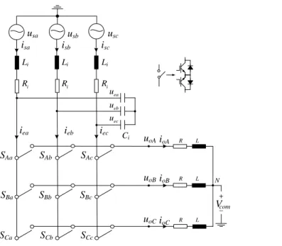
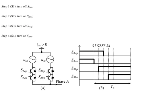
Fig. 2(a) presents a simplified circuit when the current commutates from SAa (i.e., SAap and SAan) to SAb (i.e., SAbp and SAbn),
where Sijp and Sijn (i = A, B, C; j = a, b, c) are the two quadrant switches contained in Sij. The corresponding switching process
for conventional four-step current-based commutation is shown in Fig. 2(b). The commutation relies on the current direction
information of ioA. The following four-step switching principle is adopted for ioA > 0:
Step 1 (S1): turn off SAan;
Step 2 (S2): turn on SAbp;
Step 3 (S3): turn off SAap;
Step 4 (S4): turn on SAbn.
S1
S
AapS
AanS
AbpS
AbnT
sS2 S3 S4
(
b
)
u
sau
sbS
AapS
AanS
AbpS
AbnPhase
A
i
oA> 0
(
a
)
Fig. 2. (a) A simplified DMC for explaining the switching principle of conventional four-step current-based commutation. (b) The switching process for conventional four-step current-based commutation, where S1–S4 represent the four switching steps given in Section 3.
The commutation time for a single step is denoted as td. On the basis of conventional four-step current-based commutation,
switching process for conventional four-step current-based commutation is given in Fig. 3(b). The commutation of load current
ioA is forced, and occurs in the second step of conventional four-step current-based commutation. The commutation of load
current ioB is natural, and occurs in the first step of conventional four-step current-based commutation. Thus, the commutations
for load currents ioA and ioB are not simultaneous. Rotating vectors are selected in the processes of steps 1, 3, and 4, but the
non-rotating vector “aac” appears in the process of step 2, which results in a nonzero CMV. Thus, the CMV is not always
equal to zero in a switching period.
usa usb usc
SAap SAan
SBap SBan
SAbp SAbn
SBbp SBbn
Phase C
Phase A
Phase B usa > usb , ioA > 0, ioB > 0
(a)
S1
SAap
SAan
SAbp
SAbn
SBap SBbp
SBbn
SBan
Vcom a b c
a b c
a a c
b a c
b a c
Ts (b)
S2 S3 S4
uab
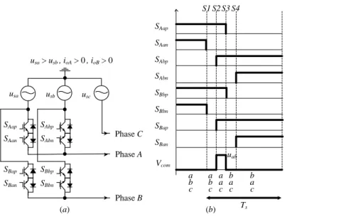
Fig. 3. (a) A simplified DMC describing the switching configuration commutating from “abc” to “bac”.
S1 SAap SAan SAbp SAbn SBap SBbp SBbn SBan Vcom a b c a b c a b c b a c b a c Ts S2 S3 S4
Delay one step
b a c S1 S2 S3 S4
Fig. 4. The switching process from “abc” to “bac” corresponding to the simplified DMC in Fig. 3(a) for the modified four-step current-based commutation, and the value of CMV obtained during commutation.
S1
S
AapS
AanS
AbpS
AbnT
s(
a
)
S2 S3 S4
case1:
u
sa>
u
sb, i
oA> 0
case2:
u
sa<
u
sb, i
oA< 0
S1
S
AapS
AanS
AbpS
AbnT
s(
b
)
S2 S3 S4
Delay one step
case3:
u
sa<
u
sb, i
oA> 0
case4:
u
sa>
u
sb, i
oA< 0
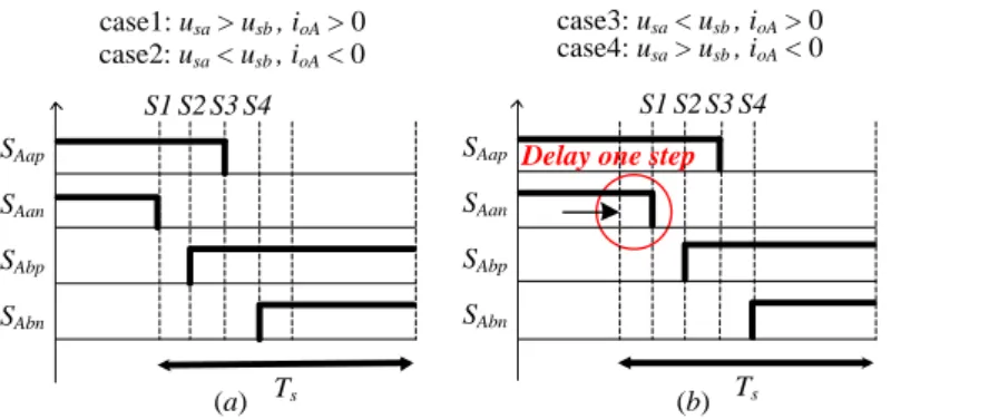
Fig. 5. The generalized switching process of the modified four-step current-based commutation in the four possible cases involving usa, usb, and ioA: (a) forced commutation; (b) natural commutation.
To achieve zero CMV, a modified four-step current-based commutation is proposed. The method intentionally delays the
natural commutation of ioB in the first step of conventional four-step current-based commutation so that it occurs
simultaneously with the forced commutation of ioA in the second step of conventional four-step current-based commutation.
The switching process of the proposed modified four-step current-based commutation is illustrated in Fig. 4 based on the
simplified DMC shown in Fig. 3(a), where, again, the switching configuration commutates from “abc” to “bac”. As observed,
the CMV is zero over TsS. Thus, the generalized switching process for the modified four-step current-based commutation in
switching processes are equivalent with conventional four-step current-based commutation. However, for cases 3 and 4
involving natural commutations, the switching processes are delayed td compared with those of conventional four-step
current-based commutation.
4.
Experimental results
In this section, based on the specifications listed in Table III, the operation and performance of the proposed simplified
FCS-MPC method were validated experimentally. As comparison, the experimental performance of an ordinary FCS-MPC
method is also given. The ordinary FCS-MPC method here refers to the one, in which all 27 possible SCs are considered. The
same cost function is used for the ordinary FCS-MPC method and the proposed simplified FCS-MPC method. The
experimental setup was developed using a floating-point digital signal controller (DSP; TMS320F28335, Texas Instruments)
and a field programmable gate array (FPGA; EP2C8T144C8N, Altera Corp.).
Table II
SPECIFICATIONS OF THE EXPERIMENTAL SETUP
Parameters Value
Supply phase RMS voltage Us (V) 60 Supply frequency fin (Hz) 50 Inductance of the line and the input filter Li (mH) 0.6 Resistance of the line and the input filter Ri (Ω) 0.1 Input filter capacitance Ci (F) 6.6 Input filter damping resistance RP (Ω) 9 Load resistance R (Ω) 4.4 Load inductance L (mH) 6 Sampling period TS (s) 70
The parameter 𝜆 in the cost function (21) are empirically adjusted. It can be adjusted from a large value, for example 2,
in order to prioritise the control of the source current. Later, it is slowly reduced, aiming to obtain low current THD both at the
input and output sides. For the presented experimental results, 0.5 is set for 𝜆.
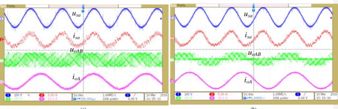
Fig. 6 shows the experimental waveforms of the source voltage usa, source current isa, output line-to-line voltage 𝑢𝑜𝐴𝐵,
and load current ioA when the DMC is operating under the proposed simplified FCS-MPC method with a reference load current
be sinusoidal with low distortions.
u
sa
u
sa
i
sa
i
sa
i
oA
i
oA
oABu
Fig. 6. Experimental results under normal conditions with the reference load current set from 5A@30Hz to 8A@60Hz
Figs. 7(a) and (b) show the input and output experimental waveforms with a reference load current of 8A@30Hz under
the ordinary and the proposed simplified FCS-MPC methods, respectively. As shown, the waveforms of isa are in phase with
those of usa, and a unity power factor is obtained. Simultaneously, ioA accurately follows the reference. The THD values of isa
and ioA obtained in the experiment are listed in Table III for reference load currents of 5A@30Hz and 8A@60Hz. From the
𝑢𝑜𝐴𝐵 waveforms, we observe that the valid SCs of the proposed FCS-MPC method are reduced relative to those of the ordinary
FCS-MPC method. The THD values for isa and ioA obtained under the proposed FCS-MPC method are a bit greater than those
of the ordinary FCS-MPC method. The computation times required by the ordinary and the proposed FCS-MPC methods are
compared in Fig. 8. The computational time of the proposed method is only 24.97 s, which is less than the 62.1 s required
for the ordinary method, therefore it is appropriate for the proposed method to be used in higher switching frequency
applications. Higher switching frequency benefits to the performance of an MPC.
u
sai
sau
oABi
oA(a)
u
sai
sau
oABi
oA(b)
Fig. 7. Input and output experimental waveforms with a reference load current of 8 A and 30 Hz: (a) the ordinary FCS-MPC
Commented [WP1]: I would prefer to see these presented
with roper axis with labels rather than as a scope screen
short – this can be done with a simple edit of the picture,
Commented [l2]: We didn’t save waveform data. It’s not
convenient to do these experiments at present since Dan
Hanbing who did the experiments are at PEMC in
method; (b) the proposed FCS-MPC method.
Fig. 8. Comparison between required running times for Algorithm A: the ordinary FCS-MPC method, and Algorithm B: the proposed simplified FCS-MPC method.
Table III
THD VALUES OF THE SOURCE CURRENT AND THE LOAD CURRENT
THD (%) Cases (8A, 30Hz, ) Cases (8A, 60Hz, ) Ordinary Proposed Ordinary Proposed isa 15 19.85 14.7 18.41 ioA 4.04 6.75 2.83 5.04
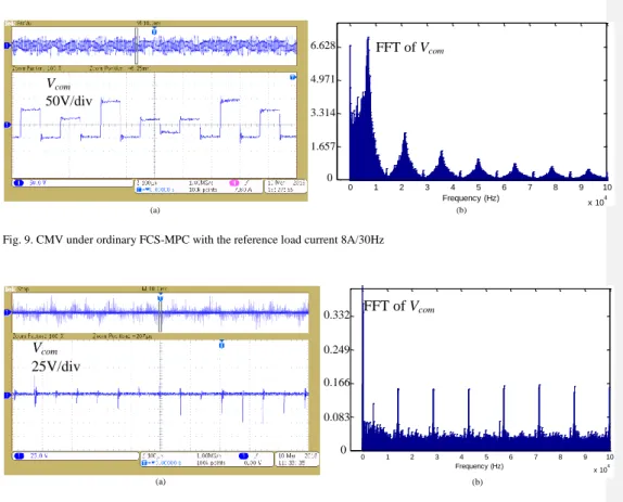
Fig. 9(a) and Fig. 10(a) show the CMV waveforms with a reference load current of 8A@60Hz under the ordinary and
proposed FCS-MPC methods, respectively. The root mean square (RMS) value of the CMV is calculated as
n 2
1
( ) com comRMS
V n V
n
(25)For the computation of VcomRMS, 100,000 points were sampled using an oscilloscope (DPO3014, Tektronix) with a sampling
frequency of 1 MHz, i.e., n = 100,000. The values of VcomRMS obtained for the ordinary and proposed FCS-MPC methods are
46.13 V and 3.29 V, respectively. Thus, the proposed FCS-MPC method reduced VcomRMS to nearly zero, and is far less than
the VcomRMS value obtained with the ordinary method. However, some CMV spikes are observed with the proposed method
during the turning-on and turning-off switching times, as shown by the Fast Fourier transform (FFT) data presented in Fig.
10(b), due to the non-ideal switching characteristics of the semiconductor switches. However these are significantly smaller
than the results without the proposed methods.
0% 20% 40% 60% 80% 100%
A B
Free
Other algorithm
FCS_MPC algorithm
(a)
0 0.01 0.02 0.03 0.04 0.05 0.06 -100
0 100
FFT window: 2 of 3 cycles of selected signal
Time (s)
0 1 2 3 4 5 6 7 8 9 10
x 104 0 100 200 300 400 Frequency (Hz)
Fundamental (30Hz) = 1.657 , THD= 2704.97%
M a g ( % o f F u n d a m e n ta
l)
FFT of
V
com(b) 0 1.657 3.314 4.971 6.628
V
com50V/div
Fig. 9. CMV under ordinary FCS-MPC with the reference load current 8A/30Hz
(a)
V
com25V/div
(a) (a)
0 0.01 0.02 0.03 0.04 0.05 0.06 -50
0 50
Time (s)
0 1 2 3 4 5 6 7 8 9 10 x 104 0 50 100 150 200 Frequency (Hz) Fundamental (30Hz) = 0.1657 , THD= 1672.98%
M a g ( % o f F u n d a m e n ta l)
FFT of
V
com(b) 0 0.083 0.166 0.249 0.332
Fig. 10. CMV under proposed FCS-MPC with the reference load current 8A/30Hz
5.
Conclusion
This paper proposes a simplified zero CMV FCS-MPC method that considers the dead-time effect as well as the modulation
process. The proposed method is simple to implement, and employs no complex calculations. In the example given in this
paper the proposed method has a computational time of only 24.97s, while that required for the ordinary FCS-MPC method
is 62.5s. Moreover, the CMV was reduced nearly to zero, and good source and load currents were obtained. Experimental
results have been presented to validate the proposed method and demonstrate the advantages.
6.
References
1. P. Wheeler, J. Rodriguez, J. Clare, L. Empringham, and A. Weinstein, "Matrix converters: A technology review",
2. T. Friedli, J.W. Kolar, J. Rodriguez, P.W. Wheeler, "Comparative evaluation of three-phase AC-AC matrix converter
and voltage dc-link back-to-back converter systems", IEEE Trans. Ind. Electron., vol. 59, no. 12, pp. 4487-4510,
2012.
3. E. Yamamoto, H. Hara, T. Uchino, M. Kawaji, T.J. Kume, J.K. Kang, H.-P. Krug, "Development of MCs and its
applications in industry", IEEE Trans. Ind. Electron., vol. 5, no. 1, pp. 4-12, 2011.
4. M. Aten, G. Tower, C. Whitley, P. Wheeler, J. Clare, and K. Bradley, “Reliability comparison of matrix and other
converter topologies” IEEE Trans. Aerosp. Electron. Syst., vol. 42, no. 3, pp. 867–875, Jul. 2006.
5. J.W. Kolar, T. Friedli, J. Rodriguez, P.W. Wheeler, "Review of three phase PWM AC–AC converter topologies",
IEEE Trans. Ind. Electron., vol. 58, no. 11, pp. 4988–5006, 2011.
6. S. Chen, T.A. Lipo, D. Fitzgerald, "Source of induction motor bearing currents caused by PWM inverters", IEEE
Trans. Energy Convers., vol. 11, no. 1, pp. 25–32, 1996.
7. J.M. Erdman, R.J. Kerkman, D.W. Schlegel, G.L. Skibinski, "Effect of PWM inverters on AC motor bearing currents
and shaft voltages", IEEE Trans. Ind. Appl., vol. 32, no. 2, pp. 250–259, 1996.
8. J. K. Kang, T. Kume, H. Hara, E. Yamamoto, "Common-mode voltage characteristics of matrix converter-driven
AC machines", Industry Applications Conference, 2005. Fourtieth IAS Annual Meeting. Conference Record of the
2005. IEEE, 2005, vol. 4, pp. 2382-2387.
9. Q. X. Guan, P. Wheeler, Q. S. Guan, and P. Yang, “Common-mode voltage reduction for matrix converters using
all valid switch states”, IEEE Transactions on Power Electronics, vol. pp, no. 99, pp: 1, 2016.
10. H. Nguyen, H. Lee, "An Enhanced SVM Method to Drive Matrix Converters for Zero Common-Mode Voltage",
IEEE Trans. Power Electrons., vol. 30, no. 4, pp. 1788-1792, 2015.
11. T. Peng, H. Dan, J. Yang et al.: "Open-switch fault diagnosis and fault tolerant for matrix converter with finite
12. S. Wei, N. Zargari, B. Wu, S. Rizzo, "Comparison and mitigation of common mode voltage in power converter
topologies", Industry Applications Conference, 2004. 39th IAS Annual Meeting. Conference Record of the 2004
IEEE, 2004, vol. 3, pp. 1852-1857.
13. M. Jussila, J. Alahuhtala, H. Tuusa, "Common-Mode Voltages of Space-Vector Modulated Matrix Converters
Compared to Three-Level Voltage Source Inverter", Power Electronics Specialists Conference, 2006. PESC '06.
37th IEEE, 2006, pp. 1-7.
14. F. Yue, P.W. Wheeler, J. Clare, "Cancellation of 3rd common mode voltage generated by matrix converter",
Industrial Electronics Society, 2005. IECON 2005. 31st Annual Conference of IEEE. IEEE, 2005, vol. 6, pp.
1217-1222.
15. S. Nath, N. Mohan, "A matrix converter fed sinusoidal input output three winding high frequency transformer with
zero common mode voltage", Power Engineering, Energy and Electrical Drives (POWERENG), 2011 International
Conference on. IEEE, 2011, pp. 1-6.
16. H.H. Lee, H.M. Nguyen, "An effective direct-SVM method for matrix converters operating with low-voltage transfer
ratio", IEEE Trans. Power Electron., vol. 28, no. 2, pp. 920-929, 2013.
17. C. Ortega, A. Arias, C. Caruana, M. Apap, "Reduction of the common mode voltage of a matrix converter fed direct
torque control", IEICE Electron., vol. 7, no. 14, pp. 1044–1050, 2010.
18. C. Ortega, A. Arias, C. Caruana, "Common mode voltage in DTC drives using matrix converters", Electronics,
Circuits and Systems, 2008. ICECS 2008. 15th IEEE International Conference on. IEEE, 2008, pp. 738-741.
19. L. Hua, H. Bi, Z. Xiaofeng, "A modulation strategy to reduce common-mode voltage for current-controlled matrix
converters", IEEE Industrial Electronics, IECON 2006-32nd Annual Conference on. IEEE, 2006, pp. 2775-2780.
20. H.J. Cha P.N. Enjeti, "An approach to reduce common-mode voltage in matrix converter", IEEE Trans. Ind. Appl.,
vol. 39, no. 4, pp. 1151–1159, 2003.
21. C. Rui, M. Su, Y. Sun, W. Gui, "A novel commutation strategy to suppress the common mode voltage for the matrix
22. L. Hong-Hee, H.M. Nguyen, T.W. Chun, "A study on rotor FOC method using matrix converter fed induction motor
with common-mode voltage reduction", Power Electronics, 2007. ICPE'07. 7th International Conference on. IEEE,
2007, pp. 159-163.
23. L. Hong-Hee, H.M. Nguyen, J. Eui-Heon, "A study on reduction of common-mode voltage in matrix converter with
unity input power factor and sinusoidal input/output waveforms", Industrial Electronics Society, 2005. IECON 2005.
31st Annual Conference of IEEE. IEEE, 2005, vol. 7, pp. 1210–1216.
24. H.M. Nguyen, H.H. Lee, "A new SVM method to reduce common-mode voltage in direct matrix converter", Power
Electronics, IPEC 2014. IEEE, 2014, pp. 1013 - 1020.
25. H. N. Nguyen, H. H. Lee,"A modulation scheme for matrix converters with perfect zero common-mode voltage",
IEEE Transactions on Power Electronics, vol.31, no. 8, pp: 5411-5422, 2016.
26. J. Rodriguez, M. P. Kazmierkowski, J. R. Espinoza, P. Zanchetta, H. Abu-Rub, H. A. Young, and C. A. Rojas, "State
of the Art of Finite Control Set Model Predictive Control in Power Electronics," IEEE Transactions on Industrial
Informatics, vol. 9, pp. 1003-1016, 2013.
27. S. Kouro, P. Cortes, R. Vargas, U. Ammann, and J. Rodriguez, "Model Predictive Control — A Simple and Powerful
Method to Control Power Converters," IEEE Transactions on Industrial Electronics, vol. 56, pp. 1826-1838, 2009.
28. S. Kouro, M. A. Perez, J. Rodriguez, A. M. Llor, and H. A. Young, “Model Predictive Control: MPC's Role in the
Evolution of Power Electronics” IEEE Industrial Electronics Magazine, vol. 9, no. 4, pp. 8-21, 2014.
29. R. Vargas, U. Ammann, J. Rodriguez, J. Pontt, "Predictive strategy to control common-mode voltage in loads fed
by matrix converters", IEEE Trans. Ind. Electron., vol. 55, no. 12, pp. 4372-4380, 2008.
30. R. Vargas, J. Rodriguez, C.A. Rojas, M. Rivera, "Predictive control of an induction machine fed by a matrix
converter with increased efficiency and reduced common-mode voltage", IEEE Trans. Energy Convers., vol. 29, no.
31. M. Rivera, J. Rodriguez, J. Espinoza, B. Wu, "Reduction of common-mode voltage in an indirect matrix converter
with imposed sinusoidal input/output waveforms", IECON 2012-38th Annual Conference on IEEE Industrial
Electronics Society. IEEE, 2012, pp. 6105-6110.
32. N. Burany, "Safe control of four-quadrant switches", Industry Applications Society Annual Meeting, 1989.
Conference Record of the 1989 IEEE. IEEE, 1989, pp: 1190-1194.
33. P. Cortes, M. P. Kazmierkowski, R. M. Kennel, D. E. Quevedo, and J. Rodriguez, “Predictive control in power