Improved performance of InSe field-effect transistors by channel
encapsulation
Guangda Liang,
1Yiming Wang,
1Lin Han,
1Zai-xing Yang,
1,2Qian Xin,
1,2Zakhar R. Kudrynskyi,
3Zakhar D. Kovalyuk,
4Amalia Patanè
3and Aimin Song
1,51Center of Nanoelectronics and School of Microelectronics, Shandong University, Jinan 250100, China 2Shenzhen Research Institute of Shandong University, Shenzhen, 518057, China
3School of Physics and Astronomy, The University of Nottingham, Nottingham NG7 2RD, UK
4Institute for Problems of Materials Science, The National Academy of Sciences of Ukraine, Chernivtsi Branch,
Chernivtsi 58001, Ukraine
5School of Electrical and Electronic Engineering, University of Manchester, Manchester M13 9PL, United Kingdom E-mail:[email protected], [email protected]
Keywords: InSe, 2D semiconductor, bias stress, PMMA encapsulation
Abstract
1. Introduction
The isolation of graphene and other two-dimensional (2D) materials has raised expectations for a revolution in electronics and optoelectronics [1-3]. However, graphene has a zero band gap, which prevents its use in many applications. Thus, continuous efforts have turned to explore other 2D materials with a band gap, such as transitional metal dichalcogenides (TMDs) [4-6], black phosphorus [7, 8], and III-VI group semiconductors [9, 10]. Among the III-VI semiconductors, InSe has emerged as a promising material due to its direct band gap over a range of layer thicknesses and light in plane electron effective mass (𝑚"#$%∗ = 0.14m0) [11]. High performance few-layered InSe
photodetectors were reported by Tamalampudi et al, demonstrating a responsivity that is four orders of magnitude higher than that of MoS2 and graphene phototransistors [12]. Also, Feng et al have reported multilayer InSe field-effect
transistors (FETs) on SiO2/Si substrate, reaching field-effect mobilities of 162 cm2V-1s-1 at room temperature[13].
These mobilities can be further increased up to 1055 cm2V-1s-1 by using poly(methyl methacrylate) (PMMA)/Al2O3 as
dielectric layer rather than SiO2 due to a significant reduction of carrier scattering by surface charged impurities and
polar phonon scattering [14].
Although layered InSe exhibits outstanding optical and electrical properties [12, 15, 16], and better resilience to oxidation under ambient conditions than many other 2D materials, the electrical stability and performance of InSe-based devices can be affected by the exposure and interaction of the InSe surface to chemical species in air, such as water or oxygen [17]. For example, Balakrishnan et al have shown that the oxidation of InSe surface in air can be induced by both thermal and photo annealing, which converts a few surface layers of InSe into In2O3, thus forming an
InSe/In2O3 heterostructure [18]. On the other hand, Feng et al have demonstrated that InSe-based FETs become
unstable under a gate bias stress due to the absorption (desorption) of oxygen and water on the InSe surface[19]. Thus, the development of techniques for improving the stability in air of InSe-based devices is critical to future applications.
encapsulate the channel of MoS2-based FETs, thus increasing the carrier mobility [4]. In this work, we use PMMA as
the channel encapsulation to improve the performance of InSe-based FETs. The electrical stability of InSe FETs is investigated in response to a constant gate bias stress (±40 V) for 300 s under ambient conditions. The encapsulation of InSe by PMMA enables the fabricated FETs with higher mobility and significantly improved electrical stability. This work offers a convenient method to improve the mobility and stability of 2D-material-based devices.
2. Methods and results
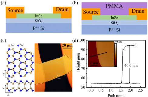
We use InSe-based FETs with and without encapsulation of the InSe layer by PMMA, as shown in figures 1(a) and 1(b). The InSe layers are prepared from bulk Bridgman-grown rhombohedral γ-InSe by mechanical exfoliation using adhesive tape and deposited on SiO2/p-Si substrates for the fabrication of InSe FETs. The primitive unit cell of γ-InSe contains three layers, each consisting of four closely-packed, covalently bonded, atomic sheets in the sequence Se-In-In-Se; within each layer plane, atoms form hexagons (figure 1(c)) [21]. The source and drain electrodes, Ti/Au (10/40 nm), are defined by shadow masks and deposited by electron-beam evaporation. For the channel encapsulation, 200 nm PMMA (950K, 4.5 wt. %) is spin-coated onto the FETs and baked at 110 oC for 2 hours. A typical optical
image of the unencapsulated InSe FET is shown in the right part of figure 1(c). This has a channel length L = 50 µm and width W = 45 µm. The corresponding thickness t of the InSe layer is approximately t = 40 nm, as measured by atomic-force microscopy (AFM) (figure 1(d)).
[image:3.612.196.440.523.684.2]respectively. (c) Left: crystal structure of InSe; Right: optical image of an InSe FET. (d) The thickness of InSe is about 40 nm, as measured by AFM. The inset is the AFM image.
The electrical performance of the fabricated back-gated FETs is characterized with a standard electrical probe station and an Agilent 2902A semiconductor analyzer. As shown by the transfer and output characteristics in figures 2a and 2b, the InSe FET shows n-type behaviour. For transfer characteristics, as shown in figure 2(a), the VGS sweep
takes 16 s (0.75 V/step), from VGS = -30 to +30 V at VDS of 0.1 V, and another 16 s for the sweep back from VGS = +30
to -30 V. Following the encapsulation of InSe by PMMA, the on current increases from 2.0 to 3.4 µA at VGS = +30 V,
and the width of the hysteresis loop decreases from 8.2 to 4.0 V. For the output characteristics, the current IDS is
measured for VDS swept from 0 to +30 V while stepping VGS from -30 to +30 V in increments of 12 V, as shown in
figure 2(b). The IDS-VDS curves indicate that fairly good ohmic contacts form between InSe and the Ti source/drain
electrodes (Ti has a work function work of 4.3 eV, slightly smaller than that of InSe around 4.6 eV).9,13 The field-effect
mobility of the InSe FETs can be extracted from the transfer curve by the equation [14, 21, 22]:
𝜇 = 𝐿 𝑊
1 𝐶-𝑉/$
d𝐼/$
d𝑉2$ (1)
where 𝐶- is the capacitance of SiO2 with a thickness of 300 nm per unit area (1.15×10⁻⁸ Fcm-2) [23]. We find that with
PMMA encapsulation, the electron mobility increases from 186 to 220 cm2V-1s-1. A similar improvement is measured
voltage VDS= 0.1 V under ambient conditions, respectively. (c) Dependence of the field-effect electron motility of InSe
FETs on the InSe layer thickness.
The electrical stability of the as-fabricated FETs is investigated by applying a constant gate bias stress (±40 V) for 300 s. The transfer characteristic curves are measured immediately after the bias stress at VDS = 1 V and at regular
time intervals. For the unencapsulated FET, after applying a gate bias stress of -40 V, the drain current increases from 26 to 30 µA at VGS = +30 V, and the threshold voltage shifts in the negative direction (∆Vth = -7.4 V), as shown in figure
3(a). After applying a gate bias stress of 40 V, the drain current decreases from 25 to 13 µA at VGS = +30 V, and the
threshold voltage increases (∆Vth = 4.3 V), as shown in figure 3(b). For the PMMA encapsulated FET, after applying
a gate bias stress of -40 V, the drain current increases from 31 to 34 µA at VGS = +30 V, and the threshold voltage
reduces (∆Vth = -3.5 V), as shown in figure 3(c). On the other hand, for a gate bias stress of +40 V, the drain current
decreases from 30 to 20 µA at VGS = +30 V, and the threshold voltage increases (∆Vth = 2.5 V), as shown in figure 3(d).
Figures 3(e) and 3(f) compare the changes of the threshold voltage and mobility for each measurement with the values of the pre-biased devices. The PMMA encapsulated FET shows much smaller shifts of the threshold voltage for both positive and negative gate bias stress than those for the FET without the encapsulation. Also, after PMMA encapsulation, the mobility is less sensitive to the gate bias stress, as shown in figure 3(f). Without PMMA encapsulation, the mobility decreases by 22.3% from 76 to 59 cm2V-1s-1 after a positive gate bias stress, and increases
by 14.4% from 76 to 87 cm2V-1s-1 after a negative gate bias stress. With PMMA encapsulation, the mobility decreases
by 13.0% from 100 to 87 cm2V-1s-1 after a positive gate bias stress, and increases by 5.0% from 100 to 105 cm2V-1s-1
Figure 3. Transfer characteristics of an unencapsulated InSe FET measured before applying the gate bias and 10 transfer curves at VDS=1 V measured after (a) -40 V and (b) +40 V gate bias stress for 300 s under ambient conditions.
Transfer characteristic of encapsulated InSe FET measured before applying the gate bias and 10 transfer curves at
VDS=1 V measured after (c) -40 V and (d) +40 V gate bias stress for 300 s under ambient conditions. (e) Threshold
voltage shifts of unencapsulated and encapsulated InSe FETs for each measurement compared with the value of pre-bias curves. (f) Field-effect mobility of unencapsulated and encapsulated InSe FETs for each measurement in linear regime following the gate bias stress.
3. Discussion
To discuss the results, we consider the energy band diagram in figure 4. Under the ideal condition, without gate bias stress, electron accumulation forms at each Ti/InSe interface because the electron affinity of InSe (~4.5 eV) is higher than the work function of Ti (~4.3 eV) [25], as shown in figure 4(a). However, under ambient condition, the InSe channel surface is subject to the adsorption of water and oxygen molecules in air [26-29]. For example, Bickley
[image:7.612.196.437.111.427.2]rutile surface and form negatively charged species (𝑂8(9): ) through the reaction: 𝑂8(;)+ 𝑒:↔ 𝑂8(9): (2)
where 𝑂8(9): donates the adsorbed oxygen on the surface and 𝑂8(;) donates the neutral oxygen in gas form [26]. Such
adsorption of oxygen has also been observed in IGZO [28-30] and MoS2 [31] devices. Lopes et al. investigated the performance a-IGZO TFT with water vapor exposure. The drain current exhibited an apparent increasing after water vapor exposure [29]. Fuh et al. further studied the effect and summarized the reaction as:
𝐻8𝑂(;)↔ 𝐻8𝑂(9)@ + 𝑒: (3)
where 𝐻8𝑂(9)@ donates the adsorbed water molecule and 𝐻8𝑂(;) donates the neutral water molecule [28], meaning
that an adsorbed water molecule can be positively charged on the channel surface by releasing an electron.
Figure 4. Schematic energy band diagrams of InSe FETs at VGS = 0 V under (a) ideal condition, (b) positive gate bias stress, and (c) negative gate bias stress conditions.
4. Conclusion
In conclusion, PMMA has been used for the channel encapsulation to improve the performance of back-gated InSe FETs in air. A number of devices with InSe channel of different thicknesses have been fabricated. All devices showed increased mobility as well as bias-stress stability after the encapsulation. The effect can be explained by the isolation of InSe channel surface from adsorption of oxygen and water in air. Our study may have implications for a better design of functional nanodevices based on two-dimensional layered materials for a wide range of device structures.
5. Acknowledgments
SYG201616), Special Foundation for Postdoctoral Innovation Projects of Shandong Province (NO. 201602017), the EU Graphene Flagship Project 604391, and the National Academy of Sciences of Ukraine.
6. REFERENCES
[1] Novoselov K S, Jiang D, Schedin F, Booth T J, Khotkevich V V, Morozov S V and Geim A K 2005 Two-dimensional atomic crystals Proceedings Of the National Academy Of Sciences Of the United States Of America102 10451-3
[2] Rogers J A, Lagally M G and Nuzzo R G 2011 Synthesis, assembly and applications of semiconductor nanomembranes Nature477 45-53
[3] Geim A K and Grigorieva I V 2013 Van der Waals heterostructures Nature499 419-25
[4] Bao W, Cai X, Kim D, Sridhara K and Fuhrer M S 2013 High mobility ambipolar MoS2 field-effect transistors: Substrate and dielectric effects Applied Physics Letters102 042104
[5] Chuang H J, Tan X, Ghimire N J, Perera M M, Chamlagain B, Cheng M M, Yan J, Mandrus D, Tomanek D and Zhou Z 2014 High mobility WSe2 p- and n-type field-effect transistors contacted by highly doped graphene for low-resistance contacts Nano Lett14 3594-601
[6] Fang H, Tosun M, Seol G, Chang T C, Takei K, Guo J and Javey A 2013 Degenerate n-doping of few-layer transition metal dichalcogenides by potassium Nano Lett13 1991-5
[7] Pan Y, Dan Y, Wang Y, Ye M, Zhang H, Quhe R, Zhang X, Li J, Guo W, Yang L and Lu J 2017 Schottky Barriers in Bilayer Phosphorene Transistors ACS Appl Mater Interfaces9 12694-705
[8] Buckley J, De Salvo B, Deleruyelle D, Gely M, Nicotra G, Lombardo S, Damlencourt J F, Hollinger P, Martin F and Deleonibus S 2005 Reduction of fixed charges in atomic layer deposited Al2O3 dielectrics Microelectronic Engineering80 210-3
[9] Mudd G W, Svatek S A, Ren T, Patane A, Makarovsky O, Eaves L, Beton P H, Kovalyuk Z D, Lashkarev G V, Kudrynskyi Z R and Dmitriev A I 2013 Tuning the bandgap of exfoliated InSe nanosheets by quantum confinement Advanced materials25 5714-8
[10] Tu H and Kelley D F 2006 Photoinduced direct electron transfer from InSe to GaSe semiconductor nanoparticles Nano Lett6 116-22
[11] Bandurin D A, Tyurnina A V, Yu G L, Mishchenko A, Zólyomi V, Morozov S V, Kumar R K, Gorbachev R V, Kudrynskyi Z R, Pezzini S, Kovalyuk Z D, Zeitler U, Novoselov K S, Patanè A, Eaves L, Grigorieva I V, Fal'ko V I, Geim A K and Cao Y 2016 High electron mobility, quantum Hall effect and anomalous optical response in atomically thin InSe Nature Nanotechnology12 223-7
[12] Tamalampudi S R, Lu Y-Y, Kumar U R, Sankar R, Liao C-D, Moorthy B K, Cheng C-H, Chou F C and Chen Y-T 2014 High Performance and bendable few-layered InSe photodetectors with broad spectral response Nano letters14 2800-6
[14] Feng W, Zheng W, Cao W and Hu P 2014 Back gated multilayer InSe transistors with enhanced carrier mobilities via the suppression of carrier scattering from a dielectric interface Advanced materials26 6587-93
[15] Lei S, Wen F, Ge L, Najmaei S, George A, Gong Y, Gao W, Jin Z, Li B, Lou J, Kono J, Vajtai R, Ajayan P and Halas N J 2015 An Atomically Layered InSe Avalanche Photodetector Nano Lett15 3048-55
[16] Lei S, Ge L, Najmaei S, George A, Kappera R, Lou J, Chhowalla M, Yamaguchi H, Gupta G, Vajtai R, Mohite A D and Ajayan P M 2014 Evolution of the Electronic Band Structure and Efficient Photo-Detection in Atomic Layers of InSe Acs Nano8 1263-72
[17] Politano A, Chiarello G, Samnakay R, Liu G, Gurbulak B, Duman S, Balandin A A and Boukhvalov D W 2016 The influence of chemical reactivity of surface defects on ambient-stable InSe-based nanodevices Nanoscale
8 8474-9
[18] Balakrishnan N, Kudrynskyi Z R, Smith E F, Fay M W, Makarovsky O, Kovalyuk Z D, Eaves L, Beton P H and Patanè A 2017 Engineering p–n junctions and bandgap tuning of InSe nanolayers by controlled oxidation 2d Mater4 025043
[19] Feng W, Zheng W, Chen X, Liu G and Hu P 2015 Gate Modulation of Threshold Voltage Instability in Multilayer InSe Field Effect Transistors ACS Appl Mater Interfaces7 26691-5
[20] Kim W, Javey A, Vermesh O, Wang Q, Li Y and Dai H 2003 Hysteresis Caused by Water Molecules in Carbon Nanotube Field-Effect Transistors Nano Letters3 193-8
[21] Sucharitakul S, Goble N J, Kumar U R, Sankar R, Bogorad Z A, Chou F C, Chen Y T and Gao X P 2015 Intrinsic Electron Mobility Exceeding 10(3) cm(2)/(V s) in Multilayer InSe FETs Nano Lett15 3815-9
[22] Kang K, Xie S E, Huang L J, Han Y M, Huang P Y, Mak K F, Kim C J, Muller D and Park J 2015 High-mobility three-atom-thick semiconducting films with wafer-scale homogeneity Nature520 656-60
[23] Zhang B, Li H, Zhang X, Luo Y, Wang Q and Song A 2015 Performance regeneration of InGaZnO transistors with ultra-thin channels Applied Physics Letters106 093506
[24] Das S, Chen H Y, Penumatcha A V and Appenzeller J 2013 High performance multilayer MoS2 transistors with scandium contacts Nano Lett13 100-5
[25] Lang O, Pettenkofer C, Sánchez-Royo J F, Segura A, Klein A and Jaegermann W 1999 Thin film growth and band lineup of In2O3 on the layered semiconductor InSe Journal of Applied Physics86 5687-91
[26] Bickley R I and Stone F S 1973 PHOTOADSORPTION AND PHOTOCATALYSIS AT RUTILE SURFACES .1. PHOTOADSORPTION OF OXYGEN Journal Of Catalysis31 389-97
[27] Park W, Park J, Jang J, Lee H, Jeong H, Cho K, Hong S and Lee T 2013 Oxygen environmental and passivation effects on molybdenum disulfide field effect transistors Nanotechnology24 095202
[28] Fuh C-S, Sze S M, Liu P-T, Teng L-F and Chou Y-T 2011 Role of environmental and annealing conditions on the passivation-free in-Ga–Zn–O TFT Thin Solid Films520 1489-94
[29] Lopes M E, Gomes H L, Medeiros M C R, Barquinha P, Pereira L, Fortunato E, Martins R and Ferreira I 2009 Gate-bias stress in amorphous oxide semiconductors thin-film transistors Applied Physics Letters95 063502 [30] Liu P-T, Chou Y-T and Teng L-F 2009 Charge pumping method for photosensor application by using
[31] Qiu H, Pan L J, Yao Z N, Li J J, Shi Y and Wang X R 2012 Electrical characterization of back-gated bi-layer MoS2 field-effect transistors and the effect of ambient on their performances Applied Physics Letters100 123104 [32] Cho K, Park W, Park J, Jeong H, Jang J, Kim T Y, Hong W K, Hong S and Lee T 2013 Electric stress-induced
threshold voltage instability of multilayer MoS2 field effect transistors Acs Nano7 7751-8