Author:
Vincent de Boer
Supervisor:
Cecilia Laborde
Chairperson:
Prof. Serge G. Lemay
Committee Member:
dr. Bernard A. Boukamp
4-7-2015
Bachelor Assignment
This bachelor Assignment report was made by Vincent de Boer, s1348736. Contact information:
Contents
1 Abstract 1
2 Introduction 2
2.1 Biosensors . . . 2
2.2 Label-Free Biosensors . . . 2
2.3 Impedance based Biosensor . . . 3
2.4 CMOS - Nano capacitor array chip . . . 3
2.5 Scope of the bachelor assignment . . . 4
3 Experimental Set-up 5 3.1 The CMOS-chip . . . 5
3.2 The socket . . . 6
4 The filter-program 7 4.1 Working of the filter-program . . . 7
4.2 Visualisation . . . 9
5 Experiment procedure 11 5.1 Pre-wash . . . 11
5.2 Capacitance measurement . . . 12
5.3 Introducing the beads/viruses-solution . . . 12
6 Results and Discussion 13 6.1 28nm Beads experiment . . . 13
6.2 AFM problems during control experiment . . . 15
6.3 CCMV experiment . . . 17
7 Conclusion 22
8 Future research 23
1 ABSTRACT
1
ABSTRACT
In this report the process of detecting of 28 nm polystyrene beads and CCMV (Cowpea Chlorotic
Mottle Virus) binding-events with a CMOS nano capacitor array from NXP are described. The purpose of this bachelor assignment is to find the limits of the CMOS nano capacitor array.
To help with the data processing a filter-program was made during this bachelor assignment to filter the data of each experiment down to a manageable size. We were successfully able to detect 28 nm polystyrene beads binding-event, however the CCMV binding-events were
much harder to detect and were only reliably detected by looking at the average binding rate of the entire array (or at least a portion of it). The AFM was used to confirm the binding-events
2 INTRODUCTION
2
INTRODUCTION
2.1 BIOSENSORS
A biosensor is a device for detecting and measuring biochemical molecules (for example: DNA,
proteins or lipids) or biochemical processes (for example: DNA replication). Many biosensors often use what is known as a ’label’ to help them to detect the molecule or process in question.
This labelling chemistry needs extra process steps and extra apparatus, which can cause the biosensors to be bulky and inefficient (long and expensive measuring time). By using
label-fee biosensors, testing can done in principle by much simpler and also cheaper devices which makes them more interesting in point-of-care applications. This means that the biosensors can be made suitable to be used in a more local environment, for example diabetes patients who
are able to check their own insulin-levels with a small diagnostic device without having to go to a hospital. In future the development of these label-free biosensors can lead to extensive
self-medication and self-diagnostics for patients and non-patients without them needing to go to a hospital. This can be especially interesting for developing countries where there is a shortage
of medical facilities.
2.2 LABEL-FREE BIOSENSORS
In most presently used biosensors, detection of specific pathogens or proteins begins by immo-bilizing appropriate bioreceptors on the sensing areas of a chip. When analytes (the molecule
you want to measure) are introduced into those areas, only the target molecules will be bound to their corresponding biomolecular receptors. This binding process is usually monitored with
commercial analytical techniques that require transduction labelling elements, such as fluores-cent dyes or radioactive isotopes, to generate a physically readable signal from a recognition
event. This is not the most preferred way because the label-indicator material can influence the biological process. Furthermore the label indicator detection is time consuming and relatively expensive. [1] [2]
2 INTRODUCTION
2.3 IMPEDANCE BASED BIOSENSOR
Impedance based biosensors measure the electrical impedance of the interface of an electrode and the solution, either by applying DC, AC-signals or a combination of the two (an AC signal
with a DC bias voltage) and measuring the resulting current. The ratio of the voltage over the current defines the impedance. This technique is known as Electrochemical Impedance Spectroscopy (EIS). When a target molecule bounds to a biomolecular receptor, this binding
can be measured by the EIS method as an impedance change of the interface of the electrode and analyte. Impedance based biosensors can therefore be utilized as label-free biosensors.
Impedance based sensors have some other major advantages over other type of sensors, the most noticeably of which is that the production of these kind of sensors can be done using the
same method as integrated circuits this means that they can be produced very compact and relatively cheap. [2] [3] [4]
2.4 CMOS - NANO CAPACITOR ARRAY CHIP
The CMOS-Nano capacitor array chip is a 90-nm CMOS-based mixed-signal capacitive biosen-sor with 256×256 densely packed nano electrodes. The sensor operates at modulation
frequen-cies up to 200 MHz, and has on-chip temperature sensors, A/D converters and digital I/O. The sensor provides a versatile platform for a multitude of novel multiplexed biosensing
applica-tions with enhanced performance by digital control and statistical data analysis. [5] [7]
In salinated environments, however, measuring distances are limited to the Debye-screening length. This screening length depends on the salt concentration for example; at 100 mMol NaCl it is 1 nm. What is happening is that the electric field from the electrode is being dampened
out by all the mobile charge carriers inside the salt solution. The mobile charge carriers form a sort of ”shield” around the electrode which electrically screens the electrode. This means that a
measurement will only happen when the protein or molecule gets closer to the electrode than the Debye-screening length. The CMOS-Nano capacitor array chip overcomes this problem by applying high frequency signals to charge and discharge the capacitor electrodes. In doing so
the ions do not have enough time to form a shield over the sensing array and thus hampers the sensing mechanism. Therefore it is possible to measure beyond the Debye-Screening-length in
2 INTRODUCTION
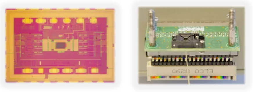
FIGURE 1:left:The CMOS capacitor array chip. right:The socket for the CMOS chip.
2.5 SCOPE OF THE BACHELOR ASSIGNMENT
The aim of the project was to explore the size-sensitivity of the CMOS Nano capacitor ar-ray platform with the ultimate goal of studying and identifying biological molecules on a
nanoscale. In order to do this, the impedance response of each electrode in the array was measured during binding of dielectric nanoparticles of different sizes in the nanometer range.
This impedance response measurement indicates a specific fingerprint of the analyte (protein or pathogen) that is being investigated. In order to corroborate if the electronic fingerprint is accurate, an Atomic Force microscope was used to verify and characterize the attached
ana-lytes. In a second stage the capabilities of detecting Cowpea Chlorotic Mottle Virus (CCMV) viruses was explored in order to see if further beneficial characteristics can be exploited of the
CMOS-Nano-capacitor-array chip. The huge amounts of data generated by the CMOS Nano capacitor array chip was at the time processed in a manual way. This was very time consuming. The subgoal of this bachelor assignment was to automate the statistical data-analysis.
3 EXPERIMENTAL SET-UP
3
EXPERIMENTAL SET-UP
3.1 THE CMOS-CHIP
The platform was developed and manufactured by NXP Semiconductors. The chip was made
using a standard 90-nm node CMOS process with after processing to cover the copper elec-trodes with a polished Au islands of about 90-nm radius. In the post processing the wafers
were cut in coupons (4×4 cm), the surface was then cleaned and sputtered with a thin Au layer (approximately 200nm thick). This Au layer was then polished away down to the original
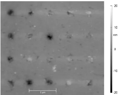
[image:8.595.106.497.288.602.2]sur-face of the chip to get the Au island of 90-nm radius covering the copper electrodes. However this last polishing step was not yet perfected so a lot of the Au islands were partially or totally ripped off, thereby exposing the under lying copper electrode again. (see figure 2)
FIGURE 2:An AFM (Atomic Force Microscope) image of an 4×5 section of the array, showing some electrodes which had their Au layer ripped off (black spots) and electrodes which still
3 EXPERIMENTAL SET-UP
As mentioned before the chip has an array of 256×256 electrodes which are spaced in a
0,6μm by 0,72μm grid pattern. The electrodes are selected row-wise and read column-wise.
During the experiments a selected row of nanocapacitors was repetitively charged/discharged at 50MHz with a modulation voltage step of 245 mV via two individual CMOS transistors using
all unselected electrodes in parallel as counter electrodes. This gives us an attofarad resolution.
3.2 THE SOCKET
To perform the measurements each individual chip was placed into a custom build test socket (CSP/μBGA Test Bum socket - Aries Electronics, Inc.). During wet-measurements the bond
pads were protected by a PDMS gasket. This created a flow cell in direct contact with the chip (and the electrode array) with a volume of about 50 nL. To introduce the liquid to the electrode
array during wet-measurements there were two 500μm holes fitted with tubing (PEEK,
inner-diameter: 125μm, outer-diameter: 510μm). [7]
4 THE FILTER-PROGRAM
4
THE FILTER-PROGRAM
During each measurement, each of the 65.536 electrode was read almost 5 times per second.
With a normal experiment being about 45 minutes long, this gave us enormous amount of data (3 to 4 GB per experiment). It was not possible for us to manually go through these large
data sets, that is why a program was made to filter the data down to a manageable size. This program filters out all the data which did not show any binding-events in the capacitance data.
4.1 WORKING OF THE FILTER-PROGRAM
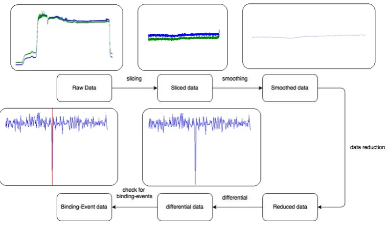
The program starts with slicing the data set down, so only the data concerning the period when
the beads/virus solution is being flushed in the flow cell is kept. This does not only saves a lot of computing time but also makes the filter-program more accurate. The flushing of different fluids with different dielectric properties into the flow cell often creates a signal which can be
misinterpreted as a binding-event. Also changing the syringes in the syringe-pump or touch-ing one of the small valves creates large spikes in the capacitance data which is very hard (if
not impossible) to filter out without also damaging any relevant data during that period. We have to turn these valves to introduce new fluids and to bleed away any air bubbles, and these
time intervals are removed.
After the slicing, the program smooths out the data to remove as much of the noise as pos-sible. It does this by applying a moving average of the data, with a span of 21. This means that
for each array element it will take the average of the 10 preceding numbers and the 10 coming numbers in the array. In the next step the program compresses the array down to a tenth of the size, for each element is now the average of the ten elements that come after it in the original
array. This save a lot of computing power and memory use without losing the relevant data, the capacitance step is still clearly visible.
From this array the program computes a differential. In this data any capacitance step will look like a large spike, either up or down, depending on the dielectric properties of the mea-sured particle. If any element of that array comes above a set number of standard deviations
(standard is 4, but it can be changed in the program’s interface) of than that point is considered a binding-event and it saves the time stamp and magnitude of the binding-event (see figure 3).
At the same time the program checks the events for any false steps. When a binding-event takes place it will show up in the differential data as a spike (see figure: 20), the direction
4 THE FILTER-PROGRAM
FIGURE 3:A flowchart showing all the steps the program takes and the effect on the data set.
differential data, only these spikes have a random orientation. The program tries to filter these out by asking the user to indicate if the analyte binding-event produces a positive or a negative
capacitance change. It treats all the other binding-events which have a different capacitance change as indicated as false binding-events and marks them red/orange (see figure: 6 and 4).
4 THE FILTER-PROGRAM
4.2 VISUALISATION
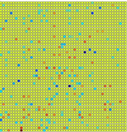
Once the program has filtered out the binding-events it displays them in a grid pattern repre-senting the real array. The data in the grid pattern is colour coded: yellow means no binding
detected, orange/red means a false step detected (this could mean that the electrode is broken, or signal interference from the measuring board), blue means binding detected, the more blue a electrode is the higher the capacitance step is (see figure 4). And one has the option to check
[image:12.595.109.516.236.658.2]the trace of each electrode to verify the programs results or to manually check each electrode for a binding-event (see figure 5 and 6).
FIGURE 4: The grid pattern with the colour coded data the program gives as a final result. Yellow means no binding detected. Orange means a false step detected, this could mean that
4 THE FILTER-PROGRAM
FIGURE 5:The main screen of the filter program where you can load the data set and set the parameters of the filter program.
FIGURE 6: The main plotting screen of the filter program, where the results of the filtering process are shown.
[image:13.595.107.517.419.679.2]5 EXPERIMENT PROCEDURE
5
EXPERIMENT PROCEDURE
5.1 PRE-WASH
Each capacitance measurement starts with flushing the flow cell with IPA (Isopropyl Alcohol)
to remove any possible dirt residue. Unfortunately removing all of the dirt without going to a clean-room environment is quite difficult and often we saw some leftover dirt particles on
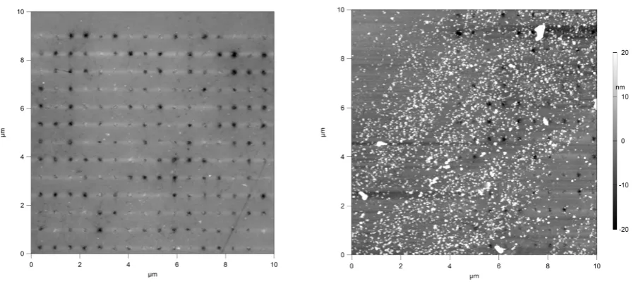
[image:14.595.105.519.236.648.2]the chip. These showed-up as white areas on the capacitance overview, meaning that those electrodes measured a lower capacitance value. (see figure 7)
FIGURE 7: A gray scale map of the real-time capacitance data of the array of the chip, each pixel here represents the real time relative capacitance value of one electrode. Areas where
there is some dirt on the array are clearly visible. The vertical stripes are normal column-wise variations due to minor offsets in the readout electronics (white areas).
5 EXPERIMENT PROCEDURE
of electrodes were lost because of dirt or simply because of failure, we could still perform a
successful experiment.
After IPA, milli-Q water was flushed into the flow cell to clear out all the IPA and the dirt residue which was dissolved into it. Next PBS was flushed solution into the flow cell. PBS,
Phosphate-Buffered Saline, is a water-based buffer solution usually containing Sodium Phos-phate and Sodium Chloride. In our case the PBS solution consisted of: 10mMol PhosPhos-phate
buffer, 2.7mMol Potassium Chloride and 137mMol Sodium Chloride. This PBS made the tran-sition smoother when the BSA, diluted in PBS, was introduced into the flow cell as the next
step. BSA, Bovine Serum Albumin, is a serum albumin protein derived from cow blood. The BSA formed a monolayer on the inside surface of the flow cell and it acted as an immobilizer protein (basically molecular glue) to stop the polystyrene beads from moving due to Brownian
motion when they were connected to the surface of the chip. After the BSA we washed PBS again to remove any leftover BSA which had not formed a monolayer in the flow cell. This
prevented the beads from sticking together before they have bonded to the surface of the chip.
5.2 CAPACITANCE MEASUREMENT
During the above ”pre-washing” procedures, the capacitance was monitored simultaneously. This was an ongoing continuous measurement (approx 5 times per second of every electrode).
However we were only interested in the capacitance measurement-data related to the binding-events; therefore only the capacitance data since the beads/viruses-solution were introduced till the moment when it was cleansed out of the flow-chip is used by the filter-program.
5.3 INTRODUCING THE BEADS/VIRUSES-SOLUTION
The solution was flowed slowly over the surface of the chip in order to give the beads/viruses
a chance to bind firmly to the surface. The beads-solution was diluted 10.000 times with PBS from the original solution we got from Life-Technologies and contained a concentration of 4
g/100mL 28 nm Polystyrene Beads (lot no.1685093). The viruses-solution was diluted 5, 10 or 20 times with PBS depending on the parameters of the experiment. The initial concentration
was 11 mg/mL CCMV viruses.
We flushed again milli-Q water through the flow-cell to get rid off all the PBS from the surface to avoid any salt-crystal-growth; because this negatively influenced the AFM (Atomic
Force Microscope)-readings afterwards.
The next step was the drying process. The chip was removed from the socket and dried with
a burst of nitrogen gas. Afterwards the chip was inserted into the AFM to check which electrode had a bead/virus stuck on top of it. The AFM readings were used as a control experiment to
verify whether the steps that were detected during the capacitance measurement were real binding-events and not just random ”noise” from the electronics-board.
6 RESULTS AND DISCUSSION
FIGURE 8:left:An area with too few beads, so almost no binding-events were observed.right:
An area with too many beads, so almost no electrodes without a binding-event and almost no
electrode with only one bead on top of it.
6
RESULTS AND DISCUSSION
6.1 28NM BEADS EXPERIMENT
We did several experiments with 28 nm beads. Most of which were however unsuccessful.
These failures occurred because there were either too many or too few beads were attached to the electrodes, both individually per electrode as per array, as revealed by the AFM-scan. The
data coming out of these over-flooded or empty electrodes was not suitable to draw meaning-ful conclusions (see figure 8). After investigation we found the cause of the failures: we either
had the beads solution for too long in the flow cell so too many beads got immobilized by the BSA or too short a time so not enough beads got immobilized by the BSA onto the surface of the chip.
After multiple experiments we did manage to get the right concentration of beads on the chip by finding the appropriate bead-solution incubation-period.
The capacitance data from a successful experiment were filtered down by the computer program and compiled into a map of the array showing which of the electrode had a binding
event and which one did not (to see the trace of a binding event, see appendix figure 18, 19 and 20). This map was compared with the AFM measurement data to see if the two maps matched
6 RESULTS AND DISCUSSION
FIGURE 9: An afm-scan overlaid with the binding map of the filter program. Yellow means no binding detected. Orange means a false binding-event detected, this could mean that the electrode is broken. Blue means binding detected, the more blue a electrode is the higher the
ca-pacitance step is. The electrode which showed the biggest step in the caca-pacitance data was elec-trode at row 4 and column 241 (see arrow) and showed a step of approx 5 attofarad (5×10⁻¹⁸ f)
The capacitance map and the AFM image matched quite well, but to verify the results we took
a ten by ten electrodes-section and analysed the capacitance data manually to check whether the computer-program did not miss any events or misinterpreted any false binding-events as real ones. False binding-binding-events are steps in the data which could look like a real
binding-event created by random noise in the electrics board. The way to distinguish them from real binding-events is that false binding-events could also be a step-increase in the data
and they usually happen to more of the electrodes in the same column or row at the exact same time. In this section the program filtered the data correctly 93% of the time. We also could see 42% of all the binding-events (the moment a beads attaches on top of an electrode) in the
capacitance data.
6 RESULTS AND DISCUSSION
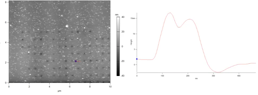
FIGURE 10:A 10×10μm AFM scan with a height trace (red line).
FIGURE 11:A 2.2×2.2μm AFM sub-scan of the same 10×10μm with a height trace (red line)
of the same beads.
6.2 AFM PROBLEMS DURING CONTROL EXPERIMENT
During the AFM control experiment we encountered very strange readings. A single bead
should have an expected height of approximately 28 nm; but this was not the case. The AFM gave data of 15 to 20 nm of height-data and this outcome even varied with the size of the
scan-area of the AFM. (see figure 10, 11 and 12)
First we considered that this size discrepancy was related with the elasticity of the beads,
that the cantilever tip of the AFM was squashing the bead during the scan. To check if this was the case an AFM scan was made using a cantilever tip with a smaller spring constant so the AFM would press so hard on the beads during the scan. However with the softer cantilever,
[image:18.595.84.534.308.496.2]6 RESULTS AND DISCUSSION
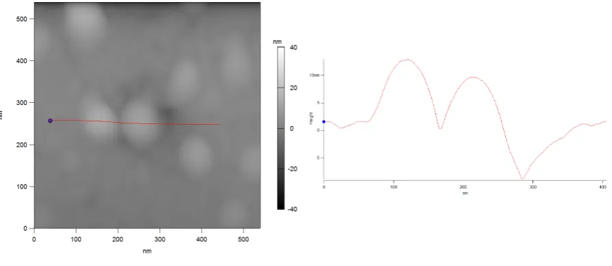
FIGURE 12:A 0.54×0.54μm AFM sub-scan of the same 10×10μm with a height trace (red line)
of the same beads.
AFM scan, a scan was made where the AFM was applying the lowest amount of force needed for a scan. But still the AFM did not show the correct height of the polystyrene beads. So the
theory that the AFM was ’crushing’ the beads during a scan was considered unlikely and new explanations were considered.
Secondly we thought that perhaps the oscillating cantilever-tip of the AFM was moving the beads around (by touching the side of the bead on each oscillation) and therefore it could never
detect the correct height of the bead, but this was also not the case because when we took an-other AFM scan of the same area all the beads proved to be at the exact same position as the
first one. Then we thought that the BSA-glue was forming a small hill whenever the cantilever-tip was pushing the bead sidewards which gave a counter force and rolled the bead back to its
original position between oscillation. By doing this the cantilever-tip would miss the opportu-nity to touch the top of the bead and therefore sensing a smaller height for the beads. But again this also proved not to be an answer because when we did the AFM-scan again but now in a
90◦offset the alleged BSA-hills were not to be found.
As a control test we performed SEM (Scanning Electron Microscope) measurements to make sure that what we imaged on the AFM were indeed the polystyrene beads and to verify the beads were in fact 28 nm (as quoted by the manufacturer). The first SEM-measurement proved
to be conclusive of the position of the beads (polystyrene) but inconclusive on the size-part (height of the beads) because the BSA on the surface of the chip was interacting with the
electron-beam of the SEM (probably burning). We match the images of the SEM with the images of the AFM to show that the ”beads” of the AFM scan were not an artefact of some
misconfiguration of the AFM. (see figure 13, 14 and 15)
6 RESULTS AND DISCUSSION
FIGURE 13:A sem image of a section of the array on the chip.All the beads seem to be covered with some kind of film so accurate size measurement is not possible with this image.
The second SEM-measurement was performed with a plain sample of dried-beads-solution on a chip (without BSA or PBS) and it showed that the beads were around 26 nm in size (see figure 16), a bit smaller than expected but bigger than the 15 to 20 nm seen by the AFM. We
then scanned this same dried sample under the AFM but again only heights of 15 to 20 nm were shown. After all this testing, we can not find an explanation yet of why the AFM measurements
lead to smaller heights. However, the SEM proved that the AFM-scan ”bleeps” were indeed caused by the polystyrene beads on the electrodes; so in this way the AFM could definitely be
used as a control experiment.
6.3 CCMV EXPERIMENT
The same problem faced with the 28 nm beads occurred with the viruses; we had either too
many or too few viruses attached to the electrodes. We managed to get just enough viruses contacting the electrodes by varying the concentration of the virus solution and varying the
6 RESULTS AND DISCUSSION
FIGURE 14:The SEM image of the top right corner of the array on the chip.
still some binding-events visible in the capacitance data when it was viewed manually but the capacitance steps were much smaller as with the 28 nm beads. And quite a few binding-events were not even visible in the capacitance data any more because the variance of the capacitance
was to small to detect. In fact these undetectable binding-events were indeed shown on the AFM image as an electrode with bead on top of it. That is how we knew we missed them.
It was however possible through statics to say for the entire array (or atleast a portion of it) that some CCMV binding-events took place. The average binding-event rate did go up
compared to an experiment with only a PBS solution with no beads or viruses but we were not able to reliably conclude that what looks like a binding-event in a trace of a single electrode is in fact a real CCMV binding-event. Maybe some fine tuning of the filter program or experimental
parameters will make it possible to reliably detect single CCMV binding-events in the future. Or perhaps we need a more sensitive electrode in order to reliably detect the binding-events
of the viruses. In the near future we expect to have access to much smaller electrodes, so we should have more sensitivity to be capable to detect the smaller capacitance variance of the viruses binding-events on a CMOS chip.
6 RESULTS AND DISCUSSION
6 RESULTS AND DISCUSSION
FIGURE 16:A SEM image of the polystyrene beads on the surface of the chip.
6 RESULTS AND DISCUSSION
FIGURE 17:An afm-scan overlaid with the binding map of the filter program. Yellow means no binding detected. Orange means a false binding-event detected, this could mean that the electrode is broken. Blue means binding detected, the more blue a electrode is the higher the
7 CONCLUSION
7
CONCLUSION
We were able to reliably detect the binding-events of 28 nm polystyrene beads in a saline
envi-ronment. These binding-events showed a maximum capacitance variance of about 5 attofarad (5×10⁻¹⁸F). The capacitance data of the binding-events was compiled into a grid pattern and
overlaid with an AFM image of the corresponding electrodes. The two images were matched and a correspondence was detected.
However during the AFM control experiment the 28 nm polystyrene beads did not show up as being 28 nm of height, but more like 15 to 20 nm depending on the scan area. We had multiple
theories as to why this was happening but none proved to be an explanation for what was hap-pening and we dismissed all of them. In the end we still do not fully understand why the 28 nm
beads appear to have a lower height on the AFM scan. We did however manage to prove that the ’beads’ that were showing on the AFM image were indeed the 28 nm polystyrene beads with the help of some SEM images. This enabled us to use the AFM as a control experiment
because we are mostly interested in the position of the beads relative to the array instead of the actual size of the beads.
The Binding-events of the CCMV viruses turned out to be much more challenging to detect
than the 28 nm polystyrene beads, because the capacitance variance of the binding-events was much lower. The filter-program we wrote and optimized to detect 28 nm polystyrene binding-events failed to detect a good enough portion of the CCMV binding-binding-events. Even when some
of the data was processed manually it was very hard to correspond the binding-events on the AFM image with the binding-events in the capacitance data. It was however possible through
statics to say for the entire array (or some part of it) that indeed some CCMV binding-events took place. The average binding-event-rate did go up compared to an experiment with only a PBS solution with no beads or viruses but we were not able to reliably conclude that what
looks like a binding-event in a trace of a single electrode is in fact a real CCMV binding-event. Maybe some fine tuning of the filter program or experimental parameters will make it possible
to reliably detect single CCMV binding-event in the future.
8 FUTURE RESEARCH
8
FUTURE RESEARCH
As said before binding-events from the 28 nm polystyrene are reliably detected but with the
CCMV most of the binding-events were overlooked by the filter program and when the data was processed manually the detection-rates were better but still not good enough. Some fine
tuning of the filter program or experimental parameters will perhaps make it possible to re-liably detect single CCMV binding-events, and is definitely worthwhile to explore in future research. In a few years we expect to have smaller and more sensitive electrodes on the CMOS
chip so detecting CCMV binding-events should become more easy.
Another field to explore in the near future is to detect multiple analytes in one experiment
by making use of specific immobilizer molecules which only immobilizes one specific analyte. The idea is to coat different parts of the array with for each section a different immobilizer
molecule and flush a solution which contains various analytes over the chip. In this way it should be possible for the CMOS chip to detect different analytes by doing only one single experiment. If this is successful then it would be a great step forward in the making of a high
9 APPENDIX
[image:27.595.99.520.123.376.2] [image:27.595.108.515.443.690.2]9
APPENDIX
FIGURE 18: A trace of the sliced data of electrode (7,38) which showed a binding-event at 21 minutes and 42 seconds.
FIGURE 19:A trace of the smoothed data of electrode (7,38) which showed a binding-event at 21 minutes and 42 seconds.
9 APPENDIX
FIGURE 20: A trace of the differential data of electrode (7,38) which showed a binding-event at 21 minutes and 42 seconds.The green lines are the standard deviation of the signal of this electrode, the yellow lines are the standard deviation of the signal of this electrode times 2 and
REFERENCES
References
[1] Miguel Holgado, Mara-Fe Lagunas and Rafael Casquel. (2008). Label-free optical biosensor
on a single chip. Available: http://spie.org/x31912.xml. Last accessed 24th March 2015
[2] Jonathan S. Daniels and Nader Pourmand. (2007). Label-Free Impedance Biosensors: Op-portunities and Challenges. Electroanalysis. 19 (12), 1239-1257
[3] Arun Manickam, Christopher Andrew Johnson, Sam Kavusi and Arjang Hassibi. (2012). Interface Design for CMOS-Integrated Electrochemical Impedance Spectroscopy (EIS)
Biosensors. Sensors. 12 (1), 14467-14488
[4] Akira Matsumoto and Yuji Miyahara. (2013). Current and emerging challenges of field ef-fect transistor based bio-sensing. Nanoscale. 5 (1), 10702
[5] F. Widdershoven, D. Van Steenwinckel, J. berfeld, T. Merelle, H. Suy, F. Jedema, R. Hoof-man, C. Tak, A. Sedzin, B. Cobelens, E. Sterckx, R. van der Werf, K. Verheyden, M. Kengen,
F. Swartjes and F. Frederix. (2010). CMOS biosensor platform. Electron Devices Meeting (IEDM), 2010 IEEE International. 1 (1), 36.1.1-36.1.4
[6] Girish S. Kulkarni and Zhaohui Zhong. (2012). Detection beyond the Debye Screening
Length in a High-Frequency Nanoelectronic Biosensor. Nano letters. 12 (1), 719-723
[7] C. Laborde, F. Pittino, H. A. Verhoeven, S. G. Lemay, L. Selmi, M. A. Jongsma and F. P.
Widdershoven. (2015). Real-time imaging of microparticles and living cells with CMOS nanocapacitor arrays. Nature. in press,