doi: 10.4236/jbise.2009.27078 Published Online November 2009 (http://www.SciRP.org/journal/jbise/).
Design of low-offset low-power CMOS amplifier for
biosensor application
Jin-Yong Zhang1,2, Lei Wang1, Bin Li2
1Institute of Biomedical and Health Engineering, Shenzhen Institutes of Advanced Technology, Chinese Academy of Sciences,
Shenzhen, China; 2School of Electronic and Information Engineering, South China University of Technology, Guangzhou,
China.
Email: [email protected]; [email protected]
Received 19 June 2009; revised 10 July 2009; accepted 13 July 2009.
ABSTRACT
A compacted and low-offset low-power CMOS am- plifier for biosensor application is presented in this paper. It includes a low offset Op-Amp and a high precision current reference. With a novel continuous- time DC offset rejection scheme, the IC achieves lower offset voltage and lower power consumption compared to previous designs. This configuration rejects large DC offset and drift that exist at the skin-electrode interface without the need of external components. The proposed amplifier has been im-plemented in SMIC 0.18-μm 1P6M CMOS technol-ogy, with an active silicon area of 100 μm by 120 μm. The back-annotated simulation results demonstrated the circuit features the systematic offset voltage less than 80 μV, the offset drift about 0.27 μV/℃ for temperature ranging from –30℃ to 100℃ and the total power dissipation consumed as low as 37.8 μW from a 1.8 V single supply. It dedicated to monitor low amplitude biomedical signals recording.
Keywords: Biomedical Integrated Circuit; CMOS Ampli- fier; Low-Offset and Low-Power; DC Offset Rejection; Biomedical Sensor
1. INTRODUCTION
Recently, there is increasing demand for portable and wearable devices to continuously monitor vital signals such as electroencephalography (EEG) and electrocar- diography (ECG), blood pressure, etc. [1]. These devices usually contain various types of biosensors. CMOS am-plifier is a crucial block at the front-end of these sensors, because most biomedical signals are characterized by their relative weak amplitude and low frequency, usually of few mV or less and the frequency below 1 kHz [2]. Meanwhile, these signals are often accompanied by large DC offset caused by skin-electrode interface. Therefore,
amplifying such weak signals requires an amplifier with low-offset and low-offset drift, which is quite challeng-ing without uschalleng-ing any trimmed components.
There are some techniques have been developed to deal with the design challenges. Alternatively, auto-zero- ing (AZ), correlated double sampling (CDS) and chop- per stabilization techniques (CHS) [3,4,5,6] are utilized in sensor amplifier design to obtain DC offset rejection and high noise performance. However, these circuits have some disadvantages such as the employment of large capacitors, either off-chip or on-chip. Furthermore, these circuits add many CMOS switches that inevitably introduce switching noise, thermal noise, residual non- linear switch errors and the CHS circuit consumes more power as circuit working in the chopping frequency. In fact these circuits were optimized for low flicker noise at the cost of higher bandwidth and worse thermal noise performance [7]. Trimming amplifier’s components is another skill, but performance of this circuit is strongly related to the on-chip components matching and it in- creases the cost.
As a result, we turned to the CMOS amplifier design using continuous-time technique for high performance and low-cost solution. In this paper, an integrated con-tinuous-time CMOS amplifier with low-offset voltage and low-power consumption was designed to meet the required biosensor. The proposed amplifier, designed in SMIC 0.18-μm CMOS technology, achieved less than 80 μV offset voltage and consumed only 37.8 μW under a 1.8 V supply. It is a good candidate for biosensor appli-cation.
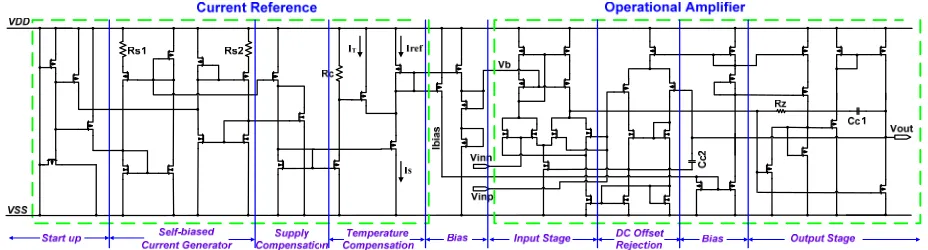
2. CIRCUIT IMPLEMENTATION
Figure 1. Architecture of the proposed integrated CMOS am-plifier.
current reference was integrated in this design, it gener-ated multiple branches of 2 μA temperature and supply independent current and were used to bias the amplifier and the bias generator. The complete schematic diagram of the proposed integrated CMOS amplifier is depicted in Figure 2.
2.1. Current Reference/Bias Generator
Minimizing the variation of the reference current and bias voltage for amplifier is crucial as well as achieving high performance in sensor systems. A novel compensa- tion scheme for supply and temperature dependency of MOSFET-only current reference was presented in this design [9]. The complete schematic of the reference is shown in Figure 2. It includes start up circuit, self-based current generator, supply and temperature compensation circuit.
The operation principle is that if two current outputs having the same dependency on supply voltage and temperature are subtracted with proper weighting, the compensation output would be obtained. As demon- strated in Figure 3, two self-biased current references generated Iout1 and Iout2, respectively.
2
1,2 2
1,2
2 1 1
(1 )
( )
out
p ox p s
I
C W L R K
(1)
Two current mirrors are adopted in this circuit to copy the currents Iout1 and Iout2 to get Im1 and Im2. The size of
the transistors and the resistance RS are determined so
the two current outputs Im1 and Im2 have the same supply
dependency and different magnitude. Then, by subtract-
ing Im2 from Im1, the supply independent output current
IS could be obtained, but it is still a function of
tempera-ture. Through a simple analysis, the supply compensated output current IS was given by:
2
1,2 2
1 2
2 1 1 1
(1 ) (1 )
( )
out
p ox p s
I
C W L R K K
2
(2)
For the negative temperature coefficients of resistor RS and μP, the supply independent current IS has a
pro-portional-to-absolute-temperature (PTAT) characteristic. The drain current of PMOSFET, IT, its temperature
coef-ficient is also positive. Then the temperature compen-sated output current IREF could be obtained by
subtract-ing IT from IS. In bias circuit, the master biasing current
and voltage of the complete amplifier were derived from the supply and temperature independent current refer-ence.
2.2. Low-Offset Operational Amplifier
Offset in operational amplifier originates in both random and systematic manner [10]. The random offset comes from imperfect fabrication of identical devices. The sys- tematic offset can be considered as errors in the design, it occurs due to the channel length modulation of tran- sistors and the magnitudes of the offset voltages are dif- ferent according to the input and output common-mode voltages [11]. In this design, a continuous-time asym- metrical differential input structure with active DC offset rejection circuit was implemented to minimize the sys- tematic offset of the amplifier [12,13].
The principle of the active DC offset rejection tech- nique is illustrated in Figure 4, considering the amplifier connected as a unity gain following configuration, where the input swing is nearly equal to the output swing. The common-mode level of the input and the output could be detected and amplified by the DC offset rejection circuit, and changed to the feedback signals for current sinks of the amplifier. This is a negative feedback network. By adjusting the current of the current sinks, the input and the output common-mode voltage would be maintained in same level to minimize the systematic offset.
As depicted in Figure 2, the circuit of low-offset
[image:2.595.66.530.576.701.2]Figure 3. The basic principle of the current reference.
Figure 4. The principle of the DC offset rejection technique.
amplifier is divided into three parts: input stage, DC offset rejection circuit, and output stage. In input stage, the input MOS transistor pairs were designed as asym- metrical differential structure. Besides, the input transis-tors and active load transistransis-tors with appropriate dimen-sions were used in order to obtain good matching char-acteristic. In DC offset rejection circuit, a single stage OTA structure was adopted to amplify the difference between input and output common-mode level. There-fore, via cascading the NMOS pairs to obtain the large gain of the OTA. In output stage, the class-AB structure was designed to improve the power efficiency, open- loop gain and driving capability. RC Miller compensa-tion and capacitor compensacompensa-tion techniques were used in this circuit [14].
Finally, a careful layout was planned to reduce proc- ess-related random offset: a) the symmetrical layout style was addressed through the entire layout, b) com- mon-centroid cross-coupling layout strategy together with poly guard rings were adopted for critical devices and c) input pairs, active mirror loads and current sources that need to be matched were selectively grouped and arranged with dummies to minimize the effect of spac-ing-dependent parameter mismatch [15].
3. SIMULATION RESULTS AND
DISCUSSIONS
This design has been implemented using the SMIC 0.18-μm CMOS 1P6M technology. Figure 5 shows the complete layout of the integrated CMOS amplifier, with total silicon area of 100 μm by 120 μm. This chip has sent to be fabricated. We will test it with real-world physiological signals in near future.
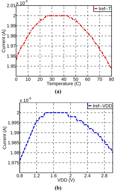
3.1. Current Reference
The temperature drifts and supply regulation of the ref- erence current are shown in Figures 6 (a) and (b), re- spectively. The reference offered a current of 2 μA when adjusted to have a zero temperature coefficient at room temperature. It could be observed that an overall tem- perature coefficient of 0.625nA/°C is obtained between 0°C and 80°C, which corresponds to about 2.2% varia- tion. The response of it is better for temperature from
Figure 5. Layout view of the integrated CMOS amplifier.
0 10 20 30 40 50 60 70 80 1.95
1.96 1.97 1.98 1.99 2 2.01x 10
-6
Temperature (C)
C
u
rre
n
t (
A
)
Iref--T
(a)
0.8 1.2 1.6 2 2.4 2.8 1.975
1.98 1.985 1.99 1.995 2
x 10-6
VDD (V)
C
u
rre
n
t (A
)
Iref--VDD
(b)
[image:3.595.56.287.206.317.2] [image:3.595.330.515.374.685.2]20°C to 50°C with a temperature coefficient of 0.13n A/°C. The line regulation of reference current is about 0.55%/V when the supply voltage ranges from 0.8 V to 3 V.
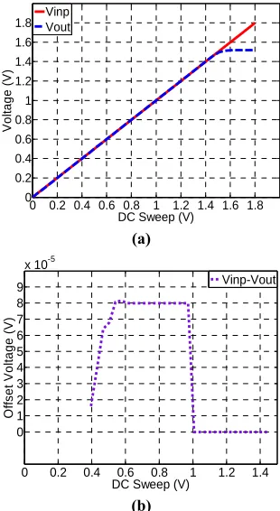
0 0.2 0.4 0.6 0.8 1 1.2 1.4 1.6 1.8
0 0.2 0.4 0.6 0.8 1 1.2 1.4 1.6 1.8
DC Sweep (V)
Vol
ta
ge (
V
)
Vinp Vout
3.2. Low-Offset Operational Amplifier
[image:4.595.346.501.80.363.2] [image:4.595.58.281.364.522.2]The performance achieved in this design was com- pared with other state-of-the-art designs for biomedical application. As listed in Table 1, it could be seen that our design offered comparable performances. The proposed Figure 7 shows the AC responses of the integrated CMOS amplifier while driving a 3 pF capacitive load. It offered 60 dB open-loop gain, 63.5°phase margin, and 2.82 MHz unity gain bandwidth. DC sweep analysis of the amplifier connected in an inverting unity-gain con-figuration is shown in Figure 8. The simulation results showed good following characteristic between Vin and Vout, and the offset voltage less than 80 μV by averag-ing. Figure 9 depicts the offset drifts of the amplifier over a wide temperature range from –30°C to 100°C. The mean offset drift is 0.24 μV/°C, it illustrated the integrated CMOS amplifier was able to sustain low off-set voltage over a wide temperature range.
(a)
0 0.2 0.4 0.6 0.8 1 1.2 1.4
0 1 2 3 4 5 6 7 8 9
x 10-5
DC Sweep (V)
Of
fs
et
Vo
lt
age
(
V
)
Vinp-Vout
(b)
Figure 8. The simulation results of the following characteristic (a)and offset tunning range (b).
-20 0 20 40 60 80 100
0 0.5 1 1.5 2 2.5 3
3.5x 10
-5
Temperature (C)
VOS (V)
[image:4.595.347.505.401.524.2]VOS-T
[image:4.595.87.510.561.723.2]Figure 7. AC simulation results of the integrated CMOS amplifier. Figure 9. The offset variation with temperature.
Table 1. Performance comparison with other publications. (*instrumentation amplifier)
Parameter Ref [5] 2002 Ref [16] 2004 Ref [17]* 2005 Ref [18] 2007 This work
CMOS Technology 0.7-μm 1.5-μm 0.35-μm 0.18-μm 0.18-μm
Supply 5 V 3 V 3~4 V 1 V 1.8 V (Typical)
Gain 60.6 dB 39.3 dB 56 dB 14 dB 60 dB
Phase Margin — — — — 63.5°
Unity Gain Bandwidth 5.5 kHz 2.7 KHz 130 KHz 2.7 KHz 2.82 MHz
CMRR 137 dB — 100 dB (@60 Hz) — >85 dB (@DC-100kHz)
PSRR — 50 dB — 50 dB >100 dB (@DC-10kHz)
Positive Slew Rate — 0.64 V/μs 50 mV/μs 10 mV/μs 3.45 V/μs
Negative Slew Rate — 0.64 V/μs 50 mV/μs 10 mV/μs 1.67 V/μs
Input Offset Voltage 88.7 μV ~811 μV 0.3 mV 1.7 mV 80 μV (max)
Offset Drift — — — — 0.27 μV/℃
Power Dissipation 11 mW 114.8 μW 72.6 μW 3.15 μW 37.8 μW
CMOS amplifier performed technical merits of low- offset voltage, reasonable low-power and with relative small die size, confirming the effectiveness and robust- ness of the proposed circuit architecture when using both circuit design technique and careful layout technique.
4. CONCLUSIONS
A low-offset low-power and compacted CMOS amplifier with continues-time active DC offset rejection design technique for biosensor applications is presented on-chip in this paper, without the need of trimming. To improve circuitry robustness over power supply and temperature, a high precision current reference was integrated in this design. The whole circuit occupies an area of 100 μm by
120 μm. The back-annotated simulation results sug-
gested that this integrated CMOS amplifier can offer significantly enhanced metrics, in terms of the low-offset less than 80μV, the offset drift about 0.27 μV/℃ for temperature ranging from –30℃ to 100℃, and the total power dissipation approximately 37.8 μW at a single 1.8 V power supply. This integrated CMOS amplifier is par- ticularly useful for a wide range of biosensor appli- cations where a front-end preamplifier is required.
REFERENCES
[1] Yazicioglu, R. F., Merken, P., and Van Hoof, C., (2005) Integrated low-power 24-channel EEG front-end, Elec- tronics Letters, 41(8), 457–458.
[2] Webster, J. G., (1998) Medical instrumentation: Applica- tion and design, 3rd Edition, Wiley, NewYork.
[3] Chan, C. H., Wills, J., LaCoss, J., Granacki, J. J., and Choma, J., (2007) A novel variable-gain micro-power band-pass auto-zeroing CMOS Amplifier, IEEE Interna- tional Symposium Circuits and Systems, 337–340,. [4] Permanod, B., Silawan, N., and Toumazou, C., (2007)
Drift reduction in Ion-sensitive FETs using correlated double sampling, IET Electronics Letter, 43(16), 857– 859.
[5] Panitantum, N. and Wongkomet, N., (2002) A low-offset high-CMRR switched-capacitor instrumentation ampli- fier for data acquisition applications, Circuits and Sys- tems, 1, 339–342.
[6] Hanasusanto, G. A. and Zheng, Y. J., (2007) A chopper stabilized pre-amplifier for biomedical signal acquisition, International Symposium on Integrated Circuits, 200–203.
[7] Li, L., (2007) High gain low power operational amplifier design and compensation techniques, A Dissertation of department of Electrical and Computer Engineering, Brigham Young University.
[8] Teo, T. H., Lim, G. K., David, D. S., Tan, K. H., Gopalakrishnan, P. K., kHz-s.l, and Singh, R., (2007) Ul-tra low-power sensor node for wireless health monitoring system, IEEE International Symposium on Circuits and Systems, 2363–2366.
[9] Yoo, C. A. and Park, J., (2007) CMOS current reference with supply and temperature compensation, Electronics Letters, 43(25), 1422–1424.
[10] Chan, P. K., Siek, L., Tay, H. C., and Su, J. H., (2000) A low-offset class-AB CMOS operational amplifier, in Proceedings, The 2000 IEEE International Symposium on Circuits and Systems, 3, 455–458.
[11] Holzmann, P. J., Wiegerink, R. J., Gierkink, S. L. J., Wassenaar, R. F., and Stroet, P., (1996) A low-offset low-voltage CMOS op amp with rail-to-rail input and output ranges, 1996 IEEE International Symposium on Circuits and Systems, 1, 179–182.
[12] Lim, K. T., Kim, S. J., and Kwon, O. K., (2003) The OP-amplifier with offset cancellation circuit, Electron Devices and Solid-State Circuits, 2003 IEEE Conference, 445–447.
[13] Gosselin, B., Ayoub, A. E., and Sawan, M., (2006) A low-power bioamplifier with a new active DC rejection scheme, in Proceedings, IEEE International Symposium on Circuits and System, 2185–2188.
[14] Hogervorst, R., Tero, J. P., Eschauzier, R. G. H., and Huijsing, J. H., (1994) A compact power-efficient 3 V CMOS rail-to-rail input/output operational amplifier for VLSI cell libraries, Solid-State Circuits, IEEE Journal, 29(12), 1505–1513.
[15] Christopher Saint and Judy Saint, IC Mask Design: Es-sential Layout Techniques, McGraw-Hill Professional, 2002.
[16] Mohseni, P. and Najafi, K., (2004) A fully integrated neural recording amplifier with DC input stabilization, Biomedical Engineering, IEEE Transactions, 51(5), 832– 837.
[17] Maryam, S. B., Rakesh, K. L., and Dinesh, K., (2005) A low-power and compact analog CMOS processing chip for portable ECG recorders, Asian Solid-State Circuits Conference, 473–476.