ISSN(Online): 2320-9801
ISSN (Print): 2320-9798
I
nternational
J
ournal of
I
nnovative
R
esearch in
C
omputer
and
C
ommunication
E
ngineering
(An ISO 3297: 2007 Certified Organization)
Vol. 4, Issue 10, October 2016
Implementation of Aging-Aware Reliable
Multiplier with Kogge-Stone Adder
P.Venkatesh1, P. Pushpa Latha2
M. Tech, Department of ECE, JNTUK, Kakinada, India1
Assistant Professor, Department of ECE, JNTUK, Kakinada, India2
ABSTRACT: We know that the most important critical arithmetic functional units in digital systems are digital multipliers. The general performance of the Digital multiplier systems depends on the multiplierthroughput. The negative bias temperature instability effect occurs to negative biased (Vgs= −Vdd)pMOS transistor, which results
increase in threshold voltage of a pMOS transistor and effecting the multiplier speed. In the same way, positive bias temperature instability occurs to nMOS transistor which is under positive bias. These two effects degrade the performance of the transistor and the system may fail due to timing violations in long term use. To reduce the performance degradation caused by these two effects, designing of reliable high-performance multipliers is very important. In this paper, we are able to design an aging-aware multiplier withnovel adaptive hold logic (AHL) circuit using kogge-stone adder. The multiplier can provide us higher throughput, less time delay and adjust the adaptive hold logic (AHL) circuit to lessen performance degradation caused due to the aging effect. The proposed design can be applied to the column bypass multiplier. Additionally, the proposed design can also be applied to row-bypassing multiplier. The experimental results show that our proposed design with the 8×8 and 16×16 row-bypassing and column-bypassing multipliers can achieve up to 3.78% and 3.94% performance improvement in total gate delay, when compared with the 8×8 and 16×16 multipliers using ripple carry adder. In addition,the 8×8 and 16×16 column-bypassing and row-column-bypassing multipliers can achieve up to6.89% and 8.28% performance improvement in total area compared with the 8×8 and 16×16 multipliers using ripple carry adder. The results also proved that proposed multiplier is very power efficient multiplier.
KEYWORDS: Aging effect, Aging indicators, Adaptive hold logic (AHL), Bias Temperature Instability, reliable multiplier, variable latency, fixed latency.
I. INTRODUCTION
Digital multipliers are the important critical arithmetic functional units in many applications, such as the FFT, DCT, and digital filtering. Multipliers performance can affect the throughput of these applications, and if the multipliers performance is slow, the performance of entire system will be reduced.
Moreover, When a pMOS transistor is under negative bias (Vgs= −Vdd)negative bias temperature instability (NBTI)[2]
occurs due to increased threshold voltage. In this circumstance, the collision or interaction between inversion layer holes and hydrogen-passivated Si atoms occurs and during oxidation process the Si–H bonds breaks, generating H or H2 molecules. When these molecules diffuse away, some gaps are left. These accumulated gaps are called as interface traps. The traps between these two layers the gate oxide interface and silicon result in increased threshold voltage (Vth),
reducing the circuit switching speed. When the negative bias is removed, the reverse reaction occurs, reducing the NBTI effect. On the other hand, the reverse reaction does not eliminate all the interface traps generated during the stress phase, and Vth is increased in the long term. Thus, it is important to design a reliable high performance multiplier.
A conventional method to moderate the aging effect is overdesign [4], [5], including such things as guard-banding and gate over-sizing; On the other hand, this advance can be very negative and area and power inefficient. These methods require circuit modification and have significant time waste. Using ripple carry adder in the multiplier will result in increased time delay. Hence, the variable- latency design with kogge-stone adder was proposed to mitigate the timing waste of traditional circuits.
ISSN(Online): 2320-9801
ISSN (Print): 2320-9798
I
nternational
J
ournal of
I
nnovative
R
esearch in
C
omputer
and
C
ommunication
E
ngineering
(An ISO 3297: 2007 Certified Organization)
Vol. 4, Issue 10, October 2016
input pattern require one or two cycles and can adjust the judging criteria to ensure that there is minimum performance degradation after considerable aging occurs.
The rest of the paper is organized as follows. Related work is explained in section II.Description of paper contribution is explained in section III.Proposed Aging-Aware Multiplier is explained in section IV. Simulation results are presented in section V. Concluding remarks are given in section VI.
II. RELATED WORK
A. COLUMN-BYPASSING MULTIPLIER
A column-bypassing multiplier is a development on the standard array multiplier (AM). The array multiplier is a fast parallel AM. The multiplier array consists of (n−1) rows of carry save adder (CSA), in which every row contains (n −
1) full adder (FA) cells. All FA in the CSA array has 2 outputs: 1) the sum bit goes down and 2) the carry bit goes to
the lower left FA. The last row is a ripple adder for carry propagation.
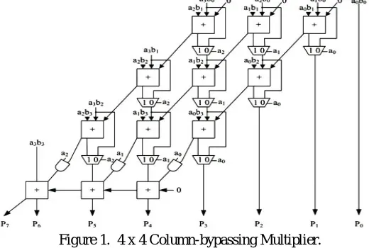
The FAs in the AM are constantly dynamic at any rate of input states. In [08], a low-power column-bypassing multiplier design is planned in which the FA operations are disabled if the consequent bit in the multiplicand is 0. Figure 1 shows a 4×4 column-bypassing multiplier. Supposing the inputs are 10102, 11112, it can be seen that for the FAs in the first and third diagonals, 2 of the 3 input bits are 0: the carry bit from its upper right FA and the partial productaibi So, the output of the adders in both diagonals is 0, and the output sum bit is merely equal to the 3rd bit,
which is the sum output of its upper FA.
Figure 1. 4 x 4 Column-bypassing Multiplier.
Therefore, the FA is modified to add two tri-state gates and one multiplexer. The multiplicand bit aican be used as the
selector of the multiplexer to decide the output of the FA, and aican also be used as the selector of the tri-state gate to
turn off the input path of the FA. If aiis 0, the inputs of FA are disabled, and the sum bit of the current FA is equal to
the sum bit from its upper FA, hence reducing the power consumption of the multiplier. If aiis 1, the normal sum result
is selected. More details for the column-bypassing multiplier can be found in [08].
B. ROW-BYPASSING MULTIPLIER
A low-power row-bypassing multiplier [9] is also planned to decrease the activity power of the AM. The process of the low-power row-bypassing multiplier is comparable to that of the low-power column-bypassing multiplier, but the selector of the multiplexers and the tri-state gates use the multiplicator.
ISSN(Online): 2320-9801
ISSN (Print): 2320-9798
I
nternational
J
ournal of
I
nnovative
R
esearch in
C
omputer
and
C
ommunication
E
ngineering
(An ISO 3297: 2007 Certified Organization)
Vol. 4, Issue 10, October 2016
Figure 2. 4 x 4 row-bypassing multiplier.
C. VARIABLE-LATENCY DESIGN
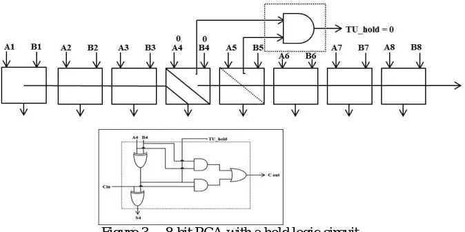
We already mentioned that the variable-latency design was proposed to minimize the timing waste by using the critical path cycle as an execution cycle period. The main concept is to execute a shorter path using a shorter cycle and longer using two cycles. Almost all paths execute in one cycle period that is much smaller than the critical path delay, this design has low average latency.Figure 3 is an 8-bit variable-latency ripple carry adder (RCA). A, B are two 8-bit inputs In RCA, and S is the 8-bit output. Let us assume the delay for each FA is one, and the maximum delay for RCA is 8.
Figure 3 . 8-bit RCA with a hold logic circuit.
Through simulation, experimental results can be determined that the possibility of the carry propagation delay being longer than 5 is very low. So let us fix the cycle period to 5, and our proposed hold logic is added to notify whether the adder can complete the addition within one cycle period.Figure 3 also shows the hold logic that is used in this circuit. Our functional logic of this hold RCA is (A4 XOR B4) (A5 XOR B5). If the output of the hold logic is 0, which
impliesA4=B4or A5 = B5, either of this adders 4and 5 will not produce a carryout.Hence, the maximum delay
encountered I our whole operation will be less than one cycle period. When the hold logic output is logic high, i.e. the input can observe paths longer than 5, so the hold logic notifies that the operation can’t be performed in one cycle and requires two cycles to complete operation.
ISSN(Online): 2320-9801
ISSN (Print): 2320-9798
I
nternational
J
ournal of
I
nnovative
R
esearch in
C
omputer
and
C
ommunication
E
ngineering
(An ISO 3297: 2007 Certified Organization)
Vol. 4, Issue 10, October 2016
latency for the variable-latency design is 0.75*5+0.25*10 = 6.25. When we compare this with the simple fixedRCA, which has 8 as an average latency, then our design can achieve a 28% performance improvement.
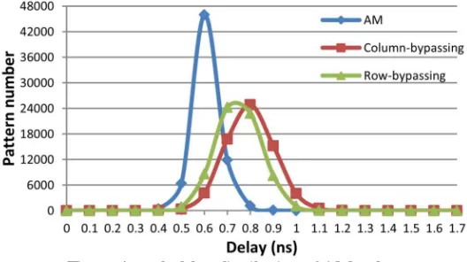
Figure 4 shows the path delay distribution of a 16 × 16 AM and for both a traditional column-bypassing and row-bypassing multipliers with 65,536 randomly chosen input patterns. Our observation shows that all multipliers execute operations on a fixed cycle period. The maximum path delay is 1.32 ns for the AM, 1.88 ns for the column-bypassing multiplier, and 1.82 ns for the row-bypassing multiplier. It can be seen that for the AM, more than 98% of the paths have a delay of <0.7 ns. Moreover, more than 93% and 98% of the paths in the normal column by-passing and row-bypassing multipliers present a delay of <0.9 ns, respectively. Hence, using the maximum path delay for these paths will have great effect on timing waste of the circuit for shorter paths, and redesigning the multiplier with variable latency can improve their performance.
Figure 4. path delay distribution of AM, column And row-bypassing multipliers for 65536 input patterns.
We can observe that number of zeros in the multiplicand in the column-bypassing multiplier is one of the most influencing factors of path delay. If the number of zeros in the multiplicands increases, and average delay will be reduced. This is so because of the multiplicand is used as the select line for column-bypassing multipliers, and higher number of zeros can skip more FAs, and the sum bi from the upper FA is directly propagates to the lower one. In
row-bypassing multiplier,the multiplicator is used as the selection line, so the multiplicator is used to determine the number of cyclesrequired to complete an operation.
We can state that the column-bypassing multiplicand and row-bypassing multiplicator are excellent parameters for our design since we can simply examine the number of zeros in the multiplicand or multiplicator to predict the number of cycles required to complete.
III. DESCRIPTION OF PAPER CONTRIBUTION
In this paper, we recommend an aging-aware reliable multiplier design with novel adaptive hold logic (AHL) circuit. The multiplier is based on the variable-latency technique and can adjust the AHL circuit to achieve reliable operation under the influence of NBTI and PBTI effects. To be detailed, the assistance of this paper is concise as follows: 1) New variable-latency multiplier design with an AHL circuit. The AHL circuit can decide whether the input patterns require one or two cycles and can adjust the judging criteria to make sure that there is minimum performance degradation after considerable aging occurs;
2) Complete analysis and comparison of the multiplier’s presentation under different cycle periods to show the efficiency of our proposed design;
3) An aging-aware reliable multiplier design technique that is appropriate for large multipliers. Even though the research is performed in 8- and 16-bit multipliers, our proposed design can be without difficulty extended to large designs;
ISSN(Online): 2320-9801
ISSN (Print): 2320-9798
I
nternational
J
ournal of
I
nnovative
R
esearch in
C
omputer
and
C
ommunication
E
ngineering
(An ISO 3297: 2007 Certified Organization)
Vol. 4, Issue 10, October 2016
using ripple carry adder. In addition,the 8×8 and 16×16 column-bypassing and row-bypassing multipliers can achieve up to6.89% and 8.28% performance improvement in total area compared with the 8×8 and 16×16 multipliers using ripple carry adder.
IV. PROPOSED AGING-AWARE MULTIPLIER
A. PROPOSED ARCHITECTURE
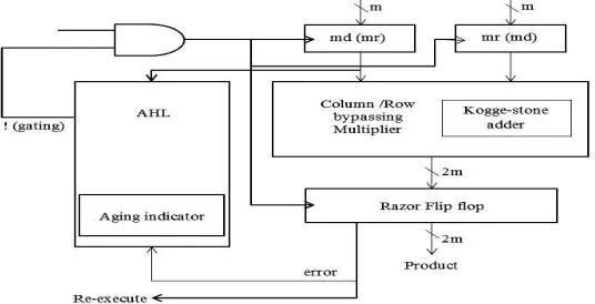
Figure 5shows our proposed aging-aware multiplier architecture, which includes two m-bit inputs (m is a positive number), one 2m-bit output, one column- or row-bypassing multiplier, 2m 1-bit Razor flip-flops [10], an AHL circuit and kogge-stone adder.
Figure 5. Proposed architecture (md- Multiplicand; mr- Multiplicator)
When input patterns are random, the number of zeros and ones in the multiplicator and multiplicand follows a normal distribution. When inputs are given to our proposed multiplier design, it gives the output to razor flip-flop. If error generated then that error signal and re-execute instruction is fed to AHL circuit. Figure 6 shows the details of the AHL circuit.In AHL circuit we have aging indicator block noting but a counter which can reset its count value after reaching its threshold value. AHL also have two judging blocks to decide which input has to be selected according to the error signal generated from the razor flip-flop
Figure 6. AHL circuit (md- Multiplicand; mr- Multiplicator)
ISSN(Online): 2320-9801
ISSN (Print): 2320-9798
I
nternational
J
ournal of
I
nnovative
R
esearch in
C
omputer
and
C
ommunication
E
ngineering
(An ISO 3297: 2007 Certified Organization)
Vol. 4, Issue 10, October 2016
Figure 7. Razor flip-flop
In future we can change the bypassing multipliers with some other multipliers to achieve furthermore advantages. In this section we describe the details of proposed multiplier using AHL with kogge-stone adder. It has the total architecture and describes the operations of each block.The AHL circuit is the key component in the aging-ware variable-latency multiplier.
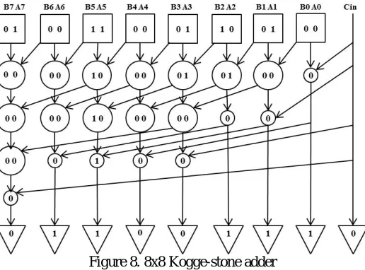
In this paper, we propose the design of multiplierusing kogge-stone adder with adaptive hold logic. Figure 8 shows kogge-stone adder process. The AHL circuit can determine which input pattern to need one or two cycles and then the circuit decides to make suitable the judging block to reduce timing waste and also low power consumption occurring in traditional circuits that use the critical path cycle as an execution cycle period. Here we are having three different blocks square, big circle, small circle, and triangle. Square box gives logical and operation and Xor operation of two inputs. Big circle gives logical or operation of one present input and logical and operation of previous inputs logical and result. Small circle just propagates the input to next stage. Triangle gives Xor operation of present input and previous input.
Figure 8. 8x8 Kogge-stone adder
ISSN(Online): 2320-9801
ISSN (Print): 2320-9798
I
nternational
J
ournal of
I
nnovative
R
esearch in
C
omputer
and
C
ommunication
E
ngineering
(An ISO 3297: 2007 Certified Organization)
Vol. 4, Issue 10, October 2016
can eliminate the aging affect caused by the effects of temperature instabilities and improves the performance of the multiplier in long term use.
V. SIMULATION RESULTS
Simulation results can be observed in below figures 9, 10 which show the RTL Schematic of aging-aware multiplier, the Simulation output waveform of the aging-aware multiplierand table 1 lists the comparison of total gate delays, area and power of the multipliers using RCA and kogge-stone adder respectively.
Figure 9.RTL schematic of Aging Aware Multiplier
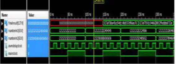
In figure 10 , output of proposed Aging Aware Multiplier is shown. Here a,b are 16-bit inputs and (D295)H,
(AF25)H are corresponding input values to multiplier. Multiplier output is represented by variable c and its value is
(90124A89)H as shown in figure10.
Figure 10.Simulation waveform of the Aging Aware Multiplier
ISSN(Online): 2320-9801
ISSN (Print): 2320-9798
I
nternational
J
ournal of
I
nnovative
R
esearch in
C
omputer
and
C
ommunication
E
ngineering
(An ISO 3297: 2007 Certified Organization)
Vol. 4, Issue 10, October 2016
Table 1. Total delays, Area and Power comparision of the multiplier usig RCA and Kogge – stone adder
Size
Delay(m.sec) Area (m.m2)
Power (m.W)
Row Column
8*8 using RCA 5.632 5.369 0.8827 1.5975
8*8 using
Kogge-Stone 5.419 5.356 0.6356 1.4682
16*16 using RCA 10.612 10.070 1.2429 2.5096
16*16 using
Kogge-stone 10.193 9.64 0.9731 1.9563
that power consumed by the overall circuit is low in proposed multiplier when compared to multiplier using RCA.
VI. CONCLUSION
Our proposed architecture with the 8×8 and 16×16 row-bypassing and column-bypassing multipliers can achieve up to 3.78% and 3.94% performance improvement in total gate delay, when compared with the 8×8 and 16×16 multipliers using ripple carry adder. In addition,the 8×8 and 16×16 column-bypassing and row-bypassing multipliers can achieve up to6.89% and 8.28% performance improvement in total area compared with the 8×8 and 16×16 multipliers using ripple carry adder.Power used by total circuit in our proposed architecture is very low when compared to previous design. Note that in addition to the BTI effect, we have some other parameter which can effect performance is interconnectionand it has its own aging issue, which is called electro migration. When the current density is high enough to cause the drift of metal ions along the direction of electron flow, electro migration occurs. The metal atoms will be gradually displaced after certain period of time, and the geometry of the wires will change. If a wire becomes narrower, the resistance and delay of the wire will be increased, and in the end, electro migration may lead to open circuits. If the aging effects caused by the BTI effect and electro migration are considered together, the delay and performance degradation of the system performance is highly effected. Fortunately, for these two effects BTI effect and electro migration, our proposed multipliers architecture can be the solution and our proposed multipliers design have less performance degradation because variable latency multipliers have less timing waste.
REFERENCES
[1] H. Abrishami, S. Hatami, B. Amelifard, and M. Pedram, “NBTI-aware flip-flop characterization and design,” in Proc. 44th ACM GLSVLSI, 2008, pp. 29–34
[2] S. V. Kumar, C. H. Kim, and S. S. Sapatnekar, “NBTI-aware synthesis of digital circuits,” in Proc. ACM/IEEE DAC, Jun. 2007, pp. 370–375. [3] A. Calimera, E. Macii, and M. Poncino, “Design techniqures for NBTI tolerant power-gating architecture,” IEEE Trans. Circuits Syst., Exp.Briefs, vol. 59, no. 4, pp. 249–253, Apr. 2012.
[4] M. Basoglu, M. Orshansky, and M. Erez, “NBTI-aware DVFS: A new approach to saving energy and increasing processor lifetime,” in
Proc.ACM/IEEE ISLPED, Aug. 2010, pp. 253–258.
[5] K.-C. Wu and D. Marculescu, “Aging-aware timing analysis and optimization considering path sensitization,” in Proc. DATE, 2011, pp. 1–6. [6] K. Du, P. Varman, and K. Mohanram, “High performance reliable variable latency carry select addition,” in Proc. DATE, 2012, pp. 1257–1262. [7] A. K. Verma, P. Brisk, and P. Ienne, “Variable latency speculative addition: A new paradigm for arithmetic circuit design,” in Proc. DATE, 2008, pp. 1250–1255.
[8] M.-C. Wen, S.-J.Wang, and Y.-N.Lin, “Low power parallel multiplier with column bypassing,” in Proc. IEEE ISCAS, May 2005, pp. 1638–1641. [9] J. Ohban, V. G. Moshnyaga, and K. Inoue, “Multiplier energy reduction through bypassing of partial products,” in Proc. APCCAS, 2002, pp. 13– 17.