Design and Implementation of Aging-Aware of
Reliable Multiplier with Adaptive Hold Logic
Gade Anusha,Pg Student
Mr.P.Sanjeeva Reddy, Professor
Malla Reddy College of Engineering & Technology,Secunderabad
ABSTRACT:
Digital multipliers are among the most critical arithmetic functional units. . Therefore, it is important to design reliable high-performance multipliers. In this paper, we propose an aging-aware multiplier design with a novel adaptive hold logic (AHL) circuit. The multiplier is able to provide higher throughput through the variable latency and can adjust the AHL circuit to mitigate performance degradation that is due to the aging effect. Moreover, the proposed architecture can be applied to a column- or row-bypassing multiplier. The experimental results show that our proposed architecture with 16 × 16 and 32 × 32 column-bypassing multipliers can attain up to 62.88% and 76.28% performance improvement, respectively, compared with 16×16 and 32×32 fixed-latency column-bypassing multipliers.
Key Terms— Adaptive hold logic (AHL), negative bias temperature instability (NBTI), positive bias temperature instability (PBTI), reliable multiplier, variable latency.
I. INTRODUCTION DIGITAL
multipliers: are among the most critical arithmetic functional units in many applications, such as the Fourier transform, discrete cosine transforms, and digital filtering. The throughput of these applications depends on
multipliers, and if the multipliers are too slow, the performance of entire circuits will be reduced. Furthermore, negative bias temperature instability (NBTI) occurs when a pMOS transistor is under negative bias (Vgs=
interaction between inversion layer holes and hydrogen-passivated Si atoms break the Si–H bond generated
during the oxidation process,
generating H or H2 molecules. When
these molecules diffuse away,
interface traps are left. The
accumulated interface traps between silicon and the gate oxide interface result in increased threshold voltage (Vth), reducing the circuit switching speed. When the biased voltage is removed, the reverse reaction occurs, reducing the NBTI effect. However, the reverse reaction does not eliminate all the interface traps generated during the stress phase, and Vthis increased in the long term. Hence, it is important to design a reliable
high-performance multiplier. The
corresponding effect on an nMOS transistor is positive bias temperature instability (PBTI), which occurs when an nMOS transistor is under positive bias. Compared with the NBTI effect, the PBTI effect is much smaller on
oxide/polygate transistors, and
therefore is usually ignored. However,
for high-k/metal-gate nMOS
transistors with significant charge trapping, the PBTI effect can no longer be ignored. In fact, it has been shown that the PBTI effect is more significant than the NBTI effect on
32-nm high-k/metalgate processes. A traditional method to mitigate the aging effect is overdesign [5], [6], including such things as
guard-banding and gate oversizing;
however, this approach can be very pessimistic and area and power inefficient. To avoid this problem,
many NBTI-aware methodologies
have been proposed. An NBTI-aware technology mapping technique was
proposed in to guarantee the
performance of the circuit during its lifetime. In], an NBTI-aware sleep transistor was designed to reduce the
aging effects on
pMOSsleeptransistors, and the
in order to perform correctly. However, the probability that the critical paths are activated is low. In most cases, the path delay is shorter than the critical path. For these noncritical paths, using the critical path delay as the overall cycle period will result in significant timing waste. Hence, the variable-latency design was proposed to reduce the timing waste of traditional circuits.
variable-latency design divides the circuit into two parts: 1) shorter paths and 2) longer paths. Shorter paths can execute correctly in one cycle, whereas longer paths need two cycles to execute. When shorter paths are activated frequently, the average latency of variable-latency designs is better than that of traditional designs. For example, several variable-latency adders were proposed using the speculation technique with error detection and recovery. A short path activation function algorithm was proposed in to improve the accuracy of the hold logic and to optimize the performance of the variable-latency circuit. An instruction scheduling algorithm was proposed into schedule the operations on nonuniform latency functional units and improve the performance of Very Long Instruction
Word processors. In, a
variable-latency pipelined multiplier
novel variable-latency multiplier architecture with an AHL circuit. The AHL circuit can decide whether the input patterns require one or two cycles and can adjust the judging criteria to ensure that there is minimum performance degradation after considerable aging occurs; 2)
comprehensive analysis and
comparison of the multiplier’s
performance under different cycle periods to show the effectiveness of our proposed architecture; 3) an aging-aware reliable multiplier design method that is suitable for large multipliers. Although the experiment is performed in 16- and 32-bit multipliers, our proposed architecture can be easily extended to large designs;
1.1AHL features.
In this paper, we propose an aging-aware reliable multiplier design with a novel adaptive hold logic (AHL) circuit. The multiplier is based on the variable-latency technique and can adjust the AHL
circuit to achieve reliable
operation under the influence of NBTI and PBTI effects. To be specific, the contributions of this paper are summarized as follows:
1) novel variable-latency
multiplier architecture with an AHL circuit. The AHL circuit can decide whether the input patterns require one or two cycles and can adjust the judging criteria to ensure that there is minimum performance degradation after considerable aging occurs;
2) comprehensive analysis and comparison of the multiplier’s performance under different cycle periods to show the effectiveness of our proposed architecture;
3) an aging-aware reliable
multiplier design method that is suitable for large multipliers.
Although the experiment is
performed in 16- and 32-bit
multipliers, our proposed
architecture can be easily extended to large designs;
4) the experimental results show that our proposed architecture with the 16 × 16 and 32 × 32 column-bypassing multipliers can attain up
to 62.88% and 76.28%
performance improvement
compared with the 16 × 16 and 32
× 32 fixed-latency
up to 80.17% and 69.40%
performance improvement as
compared with 16×16 and 32×32
fixed-latency row-bypassing
multipliers.
The paper is organized as follows.
Section II introduces the
background of the
column-bypassing multiplier,
row-bypassing multiplier, variable-latency design, and NBTI/PBTI models. Section III details the
aging-aware variable-latency
multiplier based on the column- or
rowbypassing multiplier. The
experimental setup and results are presented in Section IV. Section V concludes this paper.
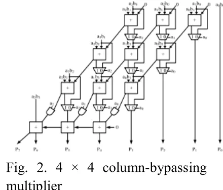
Fig. 1. 4 × 4 normal AM.
Fig. 2. 4 × 4 column-bypassing multiplier
EXISTING METHOD
Multiplication is one of the complex arithmetic operations [6]. In most of the signal processing algorithms multiplication is a root operation whereas multipliers have large area, consume considerable power and long latency. So, in low-power VLSI system design, low-power multiplier design is also an important part.
Mostly architecture of parallel multipliers can be classified into three parts: bit generation of primary partial product by using simple AND gates or by using any recoding strategies; bit compression of partial product by
using any irregular array of
logarithmic tree or by using a regular array; and the final addition [6].
for designing a new Baugh Wooley
multiplier architecture. High
Performance Multiplier (HPM)
reduction tree [6], [8] is based mainly on the generated partial product compression [1]. It is completely regular and the connectivity of the adding cells in HPM is in the triangular shape. The reason for using triangular shaped is that the triangular cell placement in the reduction tree technique has a shorter wire length [8].
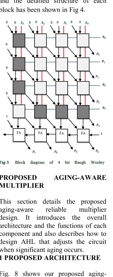
Fig-1: Illustration of 5 bit Baugh Wooley Multiplier Algorithm.
2.BAUGHWOOLEY MULTIPLIER
The Baugh-Wooley
multiplication is one of the efficient methods to handle the sign bots. This approach has been developed in order to design regular multipliers, suited for 2‘s complement numbers [2]. Let two n-bit numbers, multiplier (A) and multiplicand (B), to be multiplied. A and B can be represented as
Where the ai‘s and bi‘s are the bits in A and B, respectively, and an-1 and bn-1 are the sign bits. The product, P
by the equation:
The final product can be generated by subtracting the last two positive terms from the first two terms [2].
Instead of doing subtraction
operation, it is possible to obtain the 2‘s complement of the last two terms and add all terms to get the final product.
The last two terms are n-1 bits in which each that extend in binary weight from position 2n-1 up to 22n-3. On the other hand, the final product is 2n bits and extends in binary weight from 20 up to 22n-1. At first pad each of the last two terms in the product P equation with zeros to obtain a 2n-bit number to be able to add it with the other terms. Then the padded terms
extend in binary weight from 20 up to 22n-1 [3]. Let X is one of the last two terms that can represent it with zero padding as
The block diagram for 4 bit Baugh Wooley multiplier is shown in Fig 3 and the detailed structure of each block has been shown in Fig 4.
PROPOSED AGING-AWARE
MULTIPLIER
This section details the proposed
aging-aware reliable multiplier
design. It introduces the overall architecture and the functions of each component and also describes how to design AHL that adjusts the circuit when significant aging occurs.
1 PROPOSED ARCHITECTURE
Fig. 8 shows our proposed aging-aware multiplier architecture, which
includes two m-bit inputs (m is a positive number), one 2m-bit output,
one column- or row-bypassing
multiplier, 2m 1-bit Razor flip-flops [27], and an AHL circuit. The inputs of the row-bypassing multiplier are the symbols in the parentheses.
Fig. 8. Proposed architecture (md
means multiplicand; mr means
multiplicator).
In the proposed architecture, the
column- and row-bypassing
Hence, the two aging-aware multipliers can be implemented using
similar architecture, and the
difference between the two bypassing multipliers lies in the input signals of the AHL. According to the bypassing selection in the columnor row-bypassing multiplier, the input signal of the AHL in the architecture with the column-bypassing multiplier is the multiplicand, whereas that of the
row-bypassing multiplier is the
multiplicator. Razor flip-flops can be
used to detect whether timing
violations occur before the next input pattern arrives.
Fig. 11. Razor flip flops
Fig. 12. Diagram of AHL (md means multiplicand; mr means multiplicator)
The AHL circuit is the key
component in the aging-ware
variable-latency multiplier. Fig. 12 shows the details of the AHL circuit. The AHL circuit contains an aging indicator, two judging blocks, one mux, and one D flip-flop. The aging indicator indicates whether the circuit has suffered significant performance degradation due to the aging effect. The aging indicator is implemented in a simple counter that counts the number of errors over a certain amount of operations and is reset to zero at the end of those operations. If the cycle period is too short, the column- or row-bypassing multiplier is not able to complete these
operations successfully, causing
timing violations. These timing
violations will be caught by the Razor flip-flops, which generate error signals. If errors happen frequently and exceed a predefined threshold, it means the circuit has suffered significant timing degradation due to the aging effect, and the aging indicator will output signal 1; otherwise, it will output 0 to indicate the aging effect is still not significant, and no actions are needed.
The first judging block in the AHL circuit will output 1 if the number of
zeros in the multiplicand
(multiplicator for the row-bypassing multiplier) is larger than n (n is a positive number, which will be discussed in Section IV), and the second judging block in the AHL circuit will output 1 if the number of
zeros in the multiplicand
(multiplicator) is larger than n + 1. They are both employed to decide whether an input pattern requires one or two cycles, but only one of them will be chosen at a time. In the beginning, the aging effect is not significant, and the aging indicator produces 0, so the first judging block is used. After a period of time when the aging effect becomes significant, the second judging block is chosen. Compared with the first judging block, the second judging block allows a smaller number of patterns to become one-cycle patterns because it
requires more zeros in the
multiplicand (multiplicator)
output of the aging indicator. Then an OR operation is performed between the result of the multiplexer, and the Q¯ signal is used to determine the input of the D flip-flop. When the pattern requires one cycle, the output of the multiplexer is 1. The !(gating) signal will become 1, and the input flip flops will latch new data in the next cycle. On the other hand, when the output of the multiplexer is 0, which means the input pattern requires two cycles to complete, the OR gate will output 0 to the D flip-flop. Therefore, the !(gating) signal will be 0 to disable the clock signal of the input flip-flops in the next cycle. Note that only a cycle of the input flip-flop will be disabled because the D flip-flop will latch 1 in the next cycle.
The overall flow of our proposed architecture is as follows: when input patterns arrive, the column- or row-bypassing multiplier, and the AHL
circuit execute simultaneously.
According to the number of zeros in the multiplicand (multiplicator), the AHL circuit decides if the input patterns require one or two cycles. If the input pattern requires two cycles to complete, the AHL will output 0 to disable the clock signal of the
flip-flops. Otherwise, the AHL will output 1 for normal operations. When the column- or row-bypassing multiplier finishes the operation, the result will be passed to the Razor flip-flops. The Razor flip-flops check whether there is the path delay timing violation. If timing violations occur, it means the cycle period is not long enough for the current operation to complete and that the execution result of the multiplier is incorrect. Thus, the Razor flip-flops will output an error to inform the system that the current operation needs to be reexecuted using two cycles to ensure the operation is correct. In this situation, the extra reexecution cycles caused by timing violation incurs a penalty to overall average latency. However, our proposed AHL circuit can accurately predict whether the input patterns require one or two cycles in most cases. Only a few input patterns may cause a timing variation when the AHL circuit judges incorrectly. In this case, the extra reexecution cycles did
not produce significant timing
degradation.
noncritical paths. Second, it can provide reliable operations even after the aging effect occurs. The Razor flip-flops detect the timing violations and reexecute the operations using two cycles. Finally, our architecture can adjust the percentage of one-cycle patterns to minimize performance degradation due to the aging effect. When the circuit is aged, and many errors occur, the AHL circuit uses the second judging block to decide if an input is one cycle or two cycles.
Conclusion:
This paper proposed an aging-aware variable-latency multiplier design with the AHL. The multiplier is able to adjust the AHL to mitigate performance degradation due to increased delay. The experimental results show that our proposed architecture with 16×16 and 32×32
column-bypassing multipliers can
attain up to 62.88% and 76.28% performance improvement compared with the 16 × 16 and 32 × 32 FLCB multipliers, respectively. Furthermore, our proposed architecture with the 16×16 and 32×32 row-bypassing multipliers can achieve up to 80.17%
and 69.40% performance
improvement compared with the 16 × 16 and 32 × 32 FLRB multipliers.
REFERENCES:
[1] Y. Cao. (2013). Predictive Technology Model (PTM) and NBTI
Model [Online]. Available:
http://www.eas.asu.edu/∼ptm
[2] S. Zafar et al., “A comparative study of NBTI and PBTI (charge trapping) in SiO2/HfO2 stacks with FUSI, TiN, Re gates,” in Proc. IEEE Symp. VLSI Technol. Dig. Tech. Papers, 2006, pp. 23–25.
[3] S. Zafar, A. Kumar, E. Gusev, and
E. Cartier, “Threshold voltage
instabilities in high-k gate dielectric stacks,” IEEE Trans. Device Mater. Rel., vol. 5, no. 1, pp. 45–64, Mar. 2005.
circuits and degradation tolerant design in nanoscale CMOS SRAM,” IEEE Trans. Circuit Syst., vol. 58, no. 6, pp. 1239–1251, Jun. 2011.
[5] R. Vattikonda, W. Wang, and Y. Cao, “Modeling and miimization of pMOS NBTI effect for robust
naometer design,” in Proc.
ACM/IEEE DAC, Jun. 2004, pp. 1047–1052.
[6] H. Abrishami, S. Hatami, B. Amelifard, and M. Pedram, “NBTI-aware flip-flop characterization and
design,” in Proc. 44th ACM
GLSVLSI, 2008, pp. 29–34
[7] S. V. Kumar, C. H. Kim, and S. S. Sapatnekar, “NBTI-aware synthesis
of digital circuits,” in Proc.
ACM/IEEE DAC, Jun. 2007, pp. 370–375.
[8] A. Calimera, E. Macii, and M. Poncino, “Design techniqures for
NBTItolerant power-gating
architecture,” IEEE Trans. Circuits Syst., Exp. Briefs, vol. 59, no. 4, pp. 249–253, Apr. 2012.
[9] K.-C. Wu and D. Marculescu, “Joint logic restructuring and pin
reordering against NBTI-induced
performance degradation,” in Proc. DATE, 2009, pp. 75–80.
[10] Y. Lee and T. Kim, “A fine-grained technique of NBTI-aware voltage scaling and body biasing for standard cell based designs,” in Proc. ASPDAC, 2011, pp. 603–608.
[11] M. Basoglu, M. Orshansky, and M. Erez, “NBTI-aware DVFS: A new approach to saving energy and increasing processor lifetime,” in Proc. ACM/IEEE ISLPED, Aug. 2010, pp. 253–258.
[12] K.-C. Wu and D. Marculescu, “Aging-aware timing analysis and
optimization considering path
sensitization,” in Proc. DATE, 2011, pp. 1–6.
[13] K. Du, P. Varman, and K.
Mohanram, “High performance
reliable variable latency carry select addition,” in Proc. DATE, 2012, pp. 1257–1262.
[14] A. K. Verma, P. Brisk, and P. Ienne, “Variable latency speculative
addition: A new paradigm for
arithmetic circuit design,” in Proc. DATE, 2008, pp. 1250–1255.
[16] Y.-S. Su, D.-C.Wang, S.-C. Chang, and M. Marek-Sadowska, “Performance” optimization using variable-latency design style,” IEEE Trans. Very Large Scale Integr. (VLSI) Syst., vol. 19, no. 10, pp. 1874–1883, Oct. 2011