Design and Implementation of Aging-Aware
Reliable Multiplier by Using Carry Look-Ahead
Adder
CH.D.VishnuPriya, C.Srijana Devi
Asst. Professor, Dept of Electronics & Communication Engineering, Pragati Engineering College, Surampalem, AP, India
M.Tech Student, Dept of Electronics & Communication Engineering, Pragati Engineering College, Surampalem, AP, India
ABSTRACT: Digital multipliers are among the most critical arithmetic functional units. The overall performance of these systems depends on the throughput of the multiplier. Meanwhile, the negative bias temperature instability effect occurs when a pMOS transistor is under negative bias (Vgs = −Vdd), increasing the threshold voltage of the pMOS transistor, and reducing multiplier speed. A similar phenomenon, positive bias temperature instability, occurs when an nMOS transistor is under positive bias. Both effects degrade transistor speed, and in the long term, the system may fail due to timing violations. Therefore, it is important to design reliable high-performance multipliers. In this paper, we propose an aging-aware multiplier design with a novel adaptive hold logic (AHL) circuit. The multiplier is able to provide higher throughput through the variable latency and can adjust the AHL circuit to mitigate performance degradation that is due to the aging effect. Moreover, the proposed architecture can be applied to a column- or row-bypassing multiplier.
I.INTRODUCTION
Digital multipliers are among the most critical arithmetic functional units in many applications, such as the Fourier transform, discrete cosine transforms, and digital filtering. The through put of these applications depends on multipliers, and if the multipliers are too slow, the performance of entire circuits will be reduced. Furthermore, negative bias temperature instability (NBTI) occurs when a pMOS transistor is under negative bias (Vgs = −Vdd). In this situation, the interaction between inversion layer holes and hydrogen-passivated Si atoms breaks the Si–H bond generated during the oxidation process, generating H or H2 molecules. When these molecules diffuse away, interface traps are left.
The accumulated interface traps between silicon and the gate oxide interface result in increased threshold voltage (Vth), reducing the circuit switching speed. When the biased voltage is removed, the reverse reaction occurs, reducing the NBTI effect. However, the reverse reaction does not eliminate all the interface traps generated during the stress phase, and Vth is increased in the long term. Hence, it is important to design a reliable high-performance multiplier. The corresponding effect on an nMOS transistor is positive bias temperature instability (PBTI), which occurs when an nMOS transistor is under positive bias. Compared with the NBTI effect, the PBTI effect is much smaller on oxide/polygate transistors, and therefore is usually ignored. However, for high-k/metal-gate nMOS transistors with significant charge trapping, the PBTI effect can no longer be ignored. In fact, it has been shown that the PBTI effect is more significant than the NBTI effect on 32-nm high-k/metal-gate processes.
ISSN (Print) : 2320 – 3765 ISSN (Online): 2278 – 8875
I
nternational
J
ournal of
A
dvanced
R
esearch in
E
lectrical,
E
lectronics and
I
nstrumentation
E
ngineering
(An ISO 3297: 2007 Certified Organization)
Vol. 3, Issue 12, December 2014
pMOS sleep-transistors, and the mlifetime stability of the power-gated circuits under consideration was improved. Wu and Marculescu proposed a point logic restructuring and pin reordering method, which is based on detecting functional symmetries and transistor stacking effects. They also proposed an NBTI optimization method that considered path sensitization. In dynamic voltage scaling and body-basing techniques were proposed to reduce power or extend circuit life. These techniques, however, require circuit modification or do not provide optimization of specific circuits.
Traditional circuits use critical path delay as the overall circuit clock cycle in order to perform correctly. However, the probability that the critical paths are activated is low. In most cases, the path delay is shorter than the critical path. For these noncritical paths, using the critical path delay as the overall cycle period will result in significant timing waste. Hence, the variable-latency design was proposed to reduce the timing waste of traditional circuits. The variable-latency design divides the circuit into two parts: 1) shorter paths and 2) longer paths. Shorter paths can execute correctly in one cycle, whereas longer paths need two cycles to execute. When shorter paths are activated frequently, the average latency of variable-latency designs is better than that of traditional designs. For example, several variable-variable-latency adders were proposed using the speculation technique with error detection and recovery. A short path activation function algorithm was proposed in to improve the accuracy of the hold logic and to optimize the performance of the variable-latency circuit. An instruction scheduling algorithm was proposed in to schedule the operations on non uniform latency functional units and improve the performance of Very Long Instruction Word processors. In a variable-latency pipelined multiplier architecture with a Booth algorithm was proposed. In process-variation tolerant architecture for arithmetic units was proposed, where the effect of process-variation is considered to increase the circuit yield. In addition, the critical paths are divided into two shorter paths that could be unequal and the clock cycle is set to the delay of the longer one. These research designs were able to reduce the timing waste of traditional circuits to improve performance, but they did not consider the aging effect and could not adjust themselves during the runtime. A variable-latency adder design that considers the aging effect was proposed. However, no variable-latency multiplier design that considers the aging effect and can adjust dynamically has been done.
II.PAPER CONTRIBUTION
In this paper, we propose an aging-aware reliable multiplier design with novel adaptive hold logic (AHL) circuit. The multiplier is based on the variable-latency technique and can adjust the AHL circuit to achieve reliable operation under the influence of NBTI and PBTI effects. To be specific, the contributions of this paper are summarized as follows: 1) novel variable-latency multiplier architecture with an AHL circuit. The AHL circuit can decide whether the input patterns require one or two cycles and can adjust the judging criteria to ensure that there is minimum performance degradation after considerable aging occurs; 2) comprehensive analysis and comparison of the multiplier’s performance under different cycle periods to show the effectiveness of our proposed architecture; 3) an aging-aware reliable multiplier design method that is suitable for large multipliers. Although the experiment is performed in 16- and 32-bit multipliers, our proposed architecture can be easily extended to large designs; 4) the experimental results show that our proposed architecture with the 16 × 16 and 32 × 32 column-bypassing multipliers can attain up to 62.88% and 76.28% performance improvement compared with the 16 × 16 and 32 × 32 fixed-latency column-bypassing (FLCB) multipliers. In addition, our proposed architecture with 16 × 16 and 32 × 32 row-bypassing multipliers can achieve up to 80.17% and 69.40% performance improvement as compared with 16× 16 and 32× 32 fixed-latency row-bypassing multipliers.
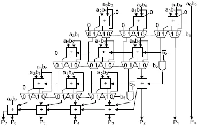
III.PRELIMINARIES
Row-Bypassing Multiplier
4 × 4 normal AM.
Fig. 3 is a 4 ×4 row-bypassing multiplier. Each input is connected to an FA through a tristate gate. When the inputs are 11112 * 10012, the two inputs in the first and second rows are 0 for FAs. Because b1 is 0, the multiplexers in the first row select aib0 as the sum bit and select 0 as the carry bit. The inputs are bypassed to FAs in the second rows, and the tristate gates turn off the input paths to the FAs.
Therefore, no switching activities occur in the first-row FAs; in return, power consumption is reduced. Similarly, because
b2is 0, no switching activities will occur in the second-row FAs. However, the FAs must be active in the third row because the b3 is not zero.
4X4 Row by passing multiplier
selector of the multiplexer to decide the output of the FA, and ai can also be used as the selector of the tristate gate to turn off the input path of the FA. If 𝑎𝑖is 0, the inputs of FA are disabled, and the sum bit of the current FA is equal to the sum bit
from its upper FA, thus reducing the power consumption of the multiplier. If 𝑎𝑖is 1, the normal sum result is selected. More
details for the column-bypassing multiplier can be found.
IV.VARIABLE-LATENCY DESIGN
ISSN (Print) : 2320 – 3765 ISSN (Online): 2278 – 8875
I
nternational
J
ournal of
A
dvanced
R
esearch in
E
lectrical,
E
lectronics and
I
nstrumentation
E
ngineering
(An ISO 3297: 2007 Certified Organization)
Vol. 3, Issue 12, December 2014
Most other arithmetic operations, e.g. multiplication and division are implemented using several add/subtract steps. Thus, improving the speed of addition will improve the speed of all other arithmetic operations.
Accordingly, reducing the carry propagation delay of adders is of great importance. Different logic design approaches have been employed to overcome the carry propagation problem.
One widely used approach employs the principle of carry look-aheadsolves this problem by calculating the carry signals in advance, based on the input signals.
This type of adder circuit is called as carry look-ahead adder (CLA adder).It is based on the fact that a carry signal will be generated in two cases:
(1) When both bits A
iand Biare 1, or
(2) When one of the two bits is 1 and the carry-in (carry of the previous stage) is 1.
The Boolean expression of the carry outputs of various stages can be written as follows:
C
1 = G0 + P0C0 C
2 = G1 + P1C1 = G1 + P1 (G0 + P0C0) = G
1 + P1G0 + P1P0C0 C
3 = G2 + P2C2 = G2 + P2G1 + P2P1G0 + P2P1P0C0 C
4 = G3 + P3C3 = G
3 + P3G2 + P3P2G1 + P3P2P1G0 + P3P2P1P0C0
In general, the i
th.
carry output is expressed in the form C
i= Fi(P’s, G’s , C0).
In other words, each carry signal is expressed as a direct SOP function of C
0 rather than its preceding carry signal.
Since the Boolean expression for each output carry is expressed in SOP form, it can be implemented in two-level circuits. The 2-level implementation of the carry signals has a propagation delay of 2 gates, i.e., 2τ.
First level: Generates all the P & G signals. Four sets of P & G logic (each consists of an XOR gate and an AND gate). Output signals of this level (P’s & G’s) will be valid after 1τ.
Second level: The Carry Look-Ahead (CLA) logic block which consists of four 2-level implementation logic circuits. It generates the carry signals (C
1, C2, C3, and C4) as defined by the above expressions. Output signals of this level (C1, C2, C3,
and C
4) will be valid after 3τ.
Third level: Four XOR gates which generate the sum signals (S
i) (Si= Pi⊕ Ci). Output signals of this level (S0, S1, S2, and
S
3) will be valid after 4τ.
Thus, the 4 Sum signals (S
0, S1, S2 & S3) will all be valid after a total delay of 4τ compared to a delay of (2n+1)τ for
Ripple Carry adders.
For a 4-bit adder (n = 4), the Ripple Carry adder delay is 9τ.
The disadvantage of the CLA adders is that the carry expressions (and hence logic) become quite complex for more than 4 bits.
V.PROPOSED AGING-AWARE MULTIPLIER
The proposed aging-aware reliable multiplier design. It introduces the overall architecture and the functions of each component and also describes how to design AHL that adjusts the circuit when significant aging occurs.
Proposed Architecture
ISSN (Print) : 2320 – 3765 ISSN (Online): 2278 – 8875
I
nternational
J
ournal of
A
dvanced
R
esearch in
E
lectrical,
E
lectronics and
I
nstrumentation
E
ngineering
(An ISO 3297: 2007 Certified Organization)
Vol. 3, Issue 12, December 2014
Proposed architecture (md means multiplicand; mr means multiplicator).
Hence, the two aging-aware multipliers can be implemented using similar architecture, and the difference between the two bypassing multipliers lies in the input signals of the AHL. According to the bypassing selection in the column or row-bypassing multiplier, the input signal of the AHL in the architecture with the column-row-bypassing multiplier is the multiplicand, whereas of the row-bypassing multiplier is the multiplicator.
Razor flip flops.
Diagram of AHL (md means multiplicand; mr means multiplicator).
Razor flip-flops can be used to detect whether timing violations occur before the next input pattern arrives.
ISSN (Print) : 2320 – 3765 ISSN (Online): 2278 – 8875
I
nternational
J
ournal of
A
dvanced
R
esearch in
E
lectrical,
E
lectronics and
I
nstrumentation
E
ngineering
(An ISO 3297: 2007 Certified Organization)
Vol. 3, Issue 12, December 2014
VI.SIMULATION RESULTS
Block diagram
RTL Schematic diagram
Simulation output waveform
VII.CONCLUSION
This paper proposed an aging-aware variable-latency multiplier design with the AHL. The multiplier is able to adjust the AHL to mitigate performance degradation due to increased delay. The experimental results show that our proposed architecture with 4x4 multiplication with CLA as last stage instead of Normal RCA adder it will decrease the delay and improve the performance compared with previous designs.
REFERENCES
[1] Y. Cao. (2013). Predictive Technology Model (PTM) and NBTI Model [Online]. Available: http://www.eas.asu.edu/∼ptm
[2] S. Zafar et al., “A comparative study of NBTI and PBTI (charge trapping) in SiO2/HfO2 stacks with FUSI, TiN, Re gates,” in Proc.
IEEE Symp. VLSI Technol. Dig. Tech. Papers, 2006, pp. 23–25.
[3] S. Zafar, A. Kumar, E. Gusev, and E. Cartier, “Threshold voltage instabilities in high-k gate dielectric stacks,” IEEE Trans. Device Mater.
Rel., vol. 5, no. 1, pp. 45–64, Mar. 2005.
[4] H.-I. Yang, S.-C. Yang, W. Hwang, and C.-T. Chuang, “Impacts of NBTI/PBTI on timing control circuits and degradation tolerant design
in nanoscale CMOS SRAM,” IEEE Trans. Circuit Syst., vol. 58, no. 6, pp. 1239–1251, Jun. 2011.
[5] R. Vattikonda, W. Wang, and Y. Cao, “Modeling and miimization of pMOS NBTI effect for robust naometer design,” in Proc. ACM/IEEE
DAC, Jun. 2004, pp. 1047–1052.
[6] H. Abrishami, S. Hatami, B. Amelifard, and M. Pedram, “NBTI-aware flip-flop characterization and design,” in Proc. 44th ACM GLSVLSI,
2008, pp. 29–34
[7] S. V. Kumar, C. H. Kim, and S. S. Sapatnekar, “NBTI-aware synthesis of digital circuits,” in Proc. ACM/IEEE DAC, Jun. 2007, pp. 370–375.
[8] A. Calimera, E. Macii, and M. Poncino, “Design techniqures for NBTItolerant power-gating architecture,” IEEE Trans. Circuits Syst., Exp.
Briefs, vol. 59, no. 4, pp. 249–253, Apr. 2012.
[9] K.-C. Wu and D. Marculescu, “Joint logic restructuring and pin reordering against NBTI-induced performance degradation,” in Proc. DATE,
2009, pp. 75–80.
[10] Y. Lee and T. Kim, “A fine-grained technique of NBTI-aware voltage scaling and body biasing for standard cell based designs,” in Proc. ASPDAC,