Design and Analysis of Boost DC-DC
Converter with Interleaved Inductor using
MPPT Algorithm
Chaitra C
1, K P Shobha 2PG Student (Power Electronic), Dept. of EEE, UVCE, Bangalore University, Bangalore, India1
Assistant Professor, Dept. of EEE, Bangalore University, Bangalore, India2
ABSTRACT: Boost converters are widely used in the low to high dc-dc applications. In the recent years, prominent efforts have been made on improving the performance and efficiency of high power boost converters. In this project, an isolated high step-up dc-dc converter with low voltage stress is explained. The proposed converter achieves extremely high voltage conversion ratio with appropriate duty cycle and reduction of voltage stress on the power devices. The topology utilizes coupled inductor. The leakage inductance energy can be efficiently discharged. Since the device stresses are low in this topology, low voltage MOSFETs with small values of RDS (on) can be selected to reduce the conduction losses. The Perturb and Observe algorithm was implemented for tracking the maximum power from the PV panel. These features improve the converter efficiency and performance. When compared to other topologies the proposed converter contain single switch which simplify the circuit configuration and improves the system reliability. All these factors improve the circuit performance in the high step-up applications.
KEYWORDS: Boost DC-DC Converter, Interleaved Inductor, MPPT Algorithm
I. INTRODUCTION
The mass usage of conventional fossil energy has resulted in reduction of fuel deposit and has affected the atmosphere causing pollution and greenhouse effect. There upraises the problem of energy shortage due to the non-renewable nature of fossil fuel energy. There is a necessity for the development of clean and non-renewable energy in order to replace conventional fossil energy. Solar energy is promising with its abundance availability and photovoltaic generation, as the utilization method has a large scale applications. Therefore, many methods have been implemented in order to improve the efficiency of the standalone PV system. Due to the non-linear characteristics of the PV panel, the maximum power from the PV panel is tracked by specific control algorithms implemented within the converter known as maximum power point tracking algorithm.
proposed converter contain single switch which simplify the circuit configuration and improve the system reliability. All these factors improve the circuit performance in the high step-up applications.
II. METHODOLOGY OF THE PROJECT
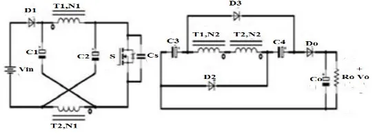
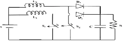
There is one coupled inductor with four windings in the converter. For the ease of understanding, it is shown in the figure 2.1 as if there are two cores, T1and T2. However, in real circuit, all coils are wound on the same core. Each coupled inductor has two windings. Turns ratios of these windings are taken as N1 and N2. Primary and secondary inductances of the coupled inductors are indicated as L1 and L2. The detailed representation of the modified converter is shown in Fig.2.1. The equivalent model of the coupled inductors includes the magnetizing inductors Lm, the primary leakage inductor Llk1, the summation secondary leakage inductor Llk2.
Fig 2.1: Circuit Diagram
The circuit also employs five capacitors (C0, C1, C2, C3 and C4), four diodes (D0, D1, D2 and D3), and a power switch (S). When the power switch is turned ON, the diodes D1, D2 and D3 are OFF while the diode Do conducts. The capacitors C1, C2, C3 and C4 are discharged, while the load capacitor Co is being charged. When the power switch is turned OFF, the diodes D1, D2 and D3 starts conducting and the diode D0 is OFF. The capacitors C1, C2, C3 and C4 are charged. While the load capacitor Co is being discharged. While the primary leakage inductance energy is discharged through the capacitors C1, C2 and the diode D1, the secondary leakage inductance energy is discharged through the load. In the meantime, the switch and the diodes do not experience extra stresses.
Basic operating principle
Before taking up this section, there are some assumptions that are to be made, 1) The turn’s ratio of the coupled inductor is low
2) The leakage inductance energy does not create stress on the switches or diodes 3) Switch voltage rating is low
4) Isolation exists between input and output
III. OPERATIONAL ANALYSIS OF DC-DC CONVERTER
Fig 3.1High step-up chopper with interleaved inductor
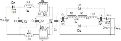
The operational analysis of the proposed DC-DC Converter can be simplified with the help of some assumptions, such as; all devices are ideal, except stray capacitance of MOSFET (Cs). The equivalent model of coupled inductor is represented by magnetizing inductance (Lm1= Lm2= Lm), leakage inductance (Llk1, Llk2) and an ideal transformer on the basis of cantilever model. Coupling co-efficient (K1 = K2 = K) and turn’s ratio N1/N2 = n. The values of capacitors (Co, C1, C2, C3 and C4) and magnetizing inductance (Lm) are too large for providing constant voltage and current over one switching period.
3.1 Continuous conduction mode (CCM)
In CCM operation, the working of circuit is divided into seven intervals. The Figure 3.2, and Figure 3.3, indicates equivalent circuit for each interval and their waveforms respectively. For CCM operation, assume that the capacitors C1, C2, C3 and C4 are charged initially.
MODE 1 : Interval [t0-t1]: In this interval, switch S is ON at t=t0, the stray capacitance Cs of S is discharged quickly. The Capacitors C1 and C2 start discharging through magnetizing inductance Lm and leakage inductance Llk1. The Lm and Llk1 are charged by voltage Vc. The currents ILm and IL1 increases linearly. The leakage inductance Llk2 discharges its energy through the capacitors C3 and C4 along with freewheeling diodes Df1 and Df2. The figure 3.2(a), indicates the equivalent circuit for this interval. The load capacitor Co is discharged through the load. In this interval input diode Din and output diode Do are off. This interval ends at t=t1 when IDf1 = IDf2 = 0.
Fig 3.2(a): Operation in Mode 1
Fig 3.2(b): Operation in Mode 2
MODE 3 : Interval [t2-t3]: In this interval, switch S is ON. The diodes D1, Df1, Df2 remains off and diode Do conduct.
All devices are retained in the same states as in interval [t1-t2]. The magnetizing inductor Lm transfers the stored energy to secondary side of coupled inductors. These coupled inductors are in series with capacitors C3 and C4. They pass energy to load through diode Do. The Fig.3.2(c),indicates the equivalent circuit for this interval. This interval ends at t=t3 when switch S is turned OFF.
Fig 3.2(c): Operation in Mode 3
MODE 4 : Interval [t3-t4]: When switch S is OFF, the stray capacitor Cs charge quickly. All other devices keep their
state as in interval [t2-t3]. This interval ends at t=t4’ when diode Din starts conducting. The Fig.3.2(d),indicates the equivalent circuit for this interval.
Fig 3.2(d): Operation in Mode 4
MODE 5 : Interval [t4-t5]: In this interval, energy stored in inductors Lm and Llk1 is discharged through source to capacitors C1 and C2. The current ILm decrease linearly. The leakage inductance Llk2 discharges its energy through capacitors C3, C4, diode Do and load. The Fig. 3.2(e),indicates the equivalent circuit for this interval. The capacitor Co is charged. In this interval, diodes Din and Do are conducting and freewheeling diodes Df1 and Df2 are off. This interval ends at t=t5 when diode Do is off.
MODE 6: Interval [t5-t6]: In this interval, energy stored in inductors Lm and Llk1 are still discharged through source to capacitors C1 and C2. The IL2 current flows through capacitors C3, C4 and freewheeling diodes Df1, Df2. The Fig. 3.2(f), indicates the equivalent circuit for this interval. The capacitors C1, C2, C3, and C4 are charged. The capacitor Co discharges its energy through load. This interval ends at t=t6 when Vl2 = nV11.
.
Fig 3.2(f): Operation of converter in Mode 6
MODE 7: Interval [t6-t7]: In this interval, switch S is OFF. In this interval all devises are in same state as in interval
[t5-t6]. The magnetizing inductor Lm transfers its storage energy to the secondary side of coupled inductors. The capacitors C3 and C4 are charged. The capacitor Co still discharges its energy through load. This interval ends at t=t7, when switch S is turned ON. The fig. 3.2(g),”indicate equivalent circuit for this interval.
Fig 3.2(g): Operation of converter in Mode 7
3.2 STEADY STATE ANALYSIS OF DC-DC CONVERTER Voltage gain in CCM intervals
The CCM is divided into seven intervals, but only two intervals is for long time. The interval [t2-t3] when switch S is ON and interval [t6-t7] switch S is OFF. The remaining intervals assume as a transient states. The one switching period is represent by Ts and Dis a duty cycle. The voltage gain equation can be obtained from “Fig. 3.2(b),” and “Fig. 3.3(e)”.In CCM, each capacitor voltage Vc1=Vc2=Vc and Vc3= Vc4 are remain constant (same for each intervals). The primary inductor voltage Vl1(on) and Vl1(off) represent for ON time and OFF time respectively. Similarly secondary inductor voltage Vl2(on) and Vl2(off)represent for ON time and OFF time respectively.
Apply KVL for ON time period
At primary side
1( ) = (1)
1= − ( ) (2)
By voltage dividing principle, ( ) = Assume = ( ) = (3)
1 = (1 − ) 2( ) = − ( )
2( ) = − (4)
Similarly, At secondary side = 3 + 4 − 2 2( ) (5)
Apply KVL on “Fig. 12(e),” for OFF time period − 1( ) =
1( )= − (6)
3 = 4 = 2 2( ) (7)
2( ) = − ( ) (8)
By applying voltage-second principle on primary inductor, ∫ 1( ) + ∫ 1( ) = 0
0
1( ) + (1 − ) 1( ) = 0
From (1) and (6) = − + + − = (9)
By applying voltage-second principle on secondary inductor, ∫ 2( ) + ∫ 2( ) = 0
0 2( ) + (1 − ) 2( ) = 0
From (4) and (8) ( ) = − [ (1 – )] (10)
Put value of (11) in (7)
3 = 4 = 2 [ (1 – )] (12) By substituting value of (4) and (12) in (5)
= 2
(13) Put value of (9) in (13) for CCM gain,
= 2 = = 2 (14) For perfect coupling K = 1,
= = (15)
VI. MPPT USING P&O ALGORITHM
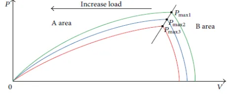
Since solar cell has a lower output voltage and current, a number of solar cells are connected in series and parallel to form PV arrays for attaining the desired PV voltage and current. Their output characteristic variations depend on ambient temperature and insolation of sun. Figure 4.1 illustrates P-V curve of PV arrays at different insolation of sun, from which it can be seen that each insolation level has a maximum power max where max1 is the most insolation of sun, while max3is the one at the least insolation. Three maximum power point max1∼ max 3 can be connect by a straight line. The operational area is divided into two areas: A area and B area. When operational point of PV arrays locates in A area, output current PV of PV arrays is decreased to make the operational point close to its maximum power point (MPP). If operational point is set in B area, current PV will be increased to operate PV arrays at its MPP. The proposed power system adopts perturb and observe method to implement MPPT. Its flowchart is shown in Figure 4.2. In Figure 4.2, and separately represent their old voltage and power, and (= ) is its new power. According to flowchart procedures of MPPT using perturb and observe method, first step is to read new voltage and current of PV arrays and then to calculate new PV power .
Fig 4.1: Plot of P-V curve for PV arrays at different isolation of sun
Fig 4.2: Flowchart of MPPT using perturb and observe method for PV arrays system
VI. STATE SPACE ANALYSIS OF THE CONVERTER
The state space analysis is the method of modeling the physical system mathematically. It relates the input, output and the state space variables using the differential equations. These differential and algebraic equations are written down in the form of the matrix. To encode all the information about the system with p inputs and q outputs one has to write down q*p Laplace transforms.
The smallest possible sub-set of system variables that represent the entire state of the system at any given time are called the state variables.
The general state-space representation of a linear system with p inputs, q outputs and n state variables is written in the following form:
Where, x (t) = state vector y (t)= output vector u (t) = input vector A= state matrix B= input matrix C= output matrix D= feed forward matrix
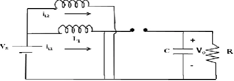
The Interleaved Boost converter consists of two single Boost converters connected in parallel. The schematic diagram of Interleaved Boost Converter is shown in Figure 5.1.
During mode 1 both the switches S1 and S2 are on and the diodes D1 and D2 are in the off condition. The equivalent circuit for this mode is shown in Figure 5.1(a).
Fig 5.1(a) Operation of interleaved Boost converter for mode 1
Applying Kirchhoff’s laws to the above circuit, the equations describing this converter for mode 1 can be obtained as follows,
The coefficient matrices for this mode can be written as,
A1= B1=
During mode 2, the switch S1is in on condition and switch S2is in off condition and the corresponding diodes
are in the complementary switching states, (i.e.) D1 is in off condition and D2 is in on condition respectively. The equivalent circuit for this mode is shown in Figure 5.1(b)
Fig 5.1(b) Operation of interleaved Boost converter for mode 2
Applying Kirchhoff’s laws to the above circuit, the equations describing this converter for mode 2 can be obtained as follows,
The coefficient matrices for this mode can be written as,
A2=
B2=
In mode 3, the switch S1is in off condition and the switch S2is in on condition and the corresponding diodes such as D1 and D2 are in on and off conditions respectively. The equivalent circuit for this mode is shown in Figure 5.1(c).
Fig 5.1(c) Operation of interleaved Boost converter for mode 3
Applying Kirchhoff’s laws to the above circuit, the equations describing this converter for mode 3 can be obtained as follows,
The coefficient matrices for this mode can be written as,
A3=
B3=
During mode 4 the semiconductor switches S1 and S2 are in off condition and the diodes D1 and D2 are in on condition, and the corresponding equivalent circuit for this mode is shown in Figure 5.1(d).
Fig 5.1(d) Operation of interleaved Boost converter for mode 4
Applying Kirchhoff’s laws to the above circuit, the equations describing this converter for mode 4 can be obtained as follows,
The coefficient matrices for this mode can be written as,
A4=
B4=
The output equation is defined as follows,
Y(t)= The coefficient matrix for the interleaved converter is defined as, [A]= (A1*D) + (A2*D) + (A3*D) + (A4*D)
[B]= (B1*D) + (B2*D) + (B3*D) + (B4*D)
D=0.28 , f =50kHz
L1=
=
= 67.2µH
L2= L1*
=67.2µH*(3/1) 2
= 604.8µH
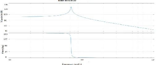
Transfer function is given by= {C [SI-A]-1 B} + D
Inverse of [SI-A] is found by Gauss Jordan Elimination Method Transfer function = C(S) 1.967*1010S R(S) S3+11.2S2+518.45*103S
Using Matlab program to find the bode plot , root locus and nyquist plot num= [ 1.967*1010 0];
den= [ 1 11.2 518.45*103 0]; sys= tf(num, den);
bode(sys);
VI. EXPERIMENTAL SETUP
6.1 SOFTWARE IMPLEMENTATION 6.1.1 SIMULATION AND ITS RESULTS
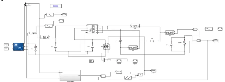
The Simulink model of the open loop of the boost DC-DC converter with interleaved inductors shown in the figure 6.1
Fig 6.1 : Simulink model of the open loop of the step up DC-DC converter
Table 6.1 Components and parameters used in simulation
Components Values
PV input voltage 19.2 volts
Irradiation 1000 rad/m2
Temperature 25oC
Frequency 50kHz
Capacitances C1,C2,C3,C4 1µF
Turns ratio of coupled inductor 2.9
Magnetizing Inductance 9.1509µH
Output Capacitance Co 1000µF
Output Resistance Ro 100Ω
Fig 6.2: Input voltage from PV panel
Fig 6.3: switching pulse across MOSFET
Fig 6.4: Output voltage wavefoRM
6.2 HARDWARE IMPLEMENTATION 6.2.1 System Model
Fig 6.5.: Block Diagram of the DC-DC Converter model
6.3 Hardware description and Working 6.3.1 Circuit Configuration
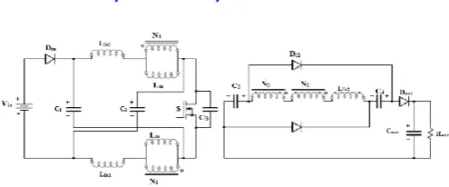
The proposed high step-up converter, is a two-phase interleaved boost converter composed of a particular magnetic coupled-inductor composed by three windings that can be installed in different core configurations. There are two winding, L1 and L2, connected to the power source and a third winding Lc, defined as central winding, located
between the cathodes of D1 and D2. For convenience, we define the positive terminal of Lc as the node where the
cathode of D1and the anode of D3are connected.
6.4 Working Principle
Fig 6.6: Hardware Model
the input and current drawn is feedback to the microcontroller. The microcontroller implements MPPT algorithm to drive the MOSFET gate voltage. The MOSFET gate is operating at a switching frequency of 40kHz.The duty cycle of the PWM is varied based on the irradiance on the solar panel. The hardware implementation of the proposed converter is shown in figure 6.6.
6.5 Hardware Results
Fig 6.7: Input from PV Panel
Fig 6.8: Switching Pulse
VII. CONCLUSION
An isolated high step-up dc-dc converter with low voltage stress is presented. The proposed converter achieves extremely large voltage conversion ratio with appropriate duty cycle and reduction of voltage stress on the power devices. The topology utilizes coupled inductor. The leakage inductance energy can efficiently be discharged. Since the device stresses are low in this topology, low voltage MOSFETs with small RDS(on) values can be selected to reduce the conduction loss. These features improve the converter efficiency. When compared to other topologies the proposed converter contain only one switch which simplify the circuit configuration and improve the system reliability. All these factors improve the circuit performance in the high step-up applications.
Isolated DC-DC boost converter sourced by a PV panel was simulated by MPPT algorithm. The P&O algorithm implemented was found successful in tracking the maximum power from the PV panel. The switching losses will be less when compared to conventional topologies since less number of power electronic switches are used. Due to coupled inductor isolation is present between input and output. The overall efficiency of the proposed chopper circuit is higher than that of the existing topologies.
REFERENCES
1. Parvathi Mohan, Sreeja E A, “ A Step up DC-DC Converter with Coupled Inductor for Renewable Energy Applications using MPPT”, International Journal of Science and Research (IJSR) ISSN (Online): 2319-7064 Volume 4 Issue 11, November 2015
2. G. Jessie Gifty Jothi and Dr. N. Geetha, “An enhanced MPPT technique for high gain DC- DC converter for photovoltaic applications”, International Conference on Circuit, Power and Computing Technologies [ICCPCT], 978-1-5090-1277-0/16/$31.00 ©2016 IEEE
3. Michael Njoroge Gitau, Fredrick Mukundi Mwaniki, and Ivan W. Hofsajer, “Analysis and Design of a Single-Phase Tapped-Coupled-Inductor Boost DC–DC Converter”, Journal of Power Electronics, Vol. 13, No. 4, July 2013
4. B.Muthuselvi and Abirami.A, “Newly Configured High Step-Up Chopper with Coupled Inductor and Voltage Doublers Circuits”, International Journal of Electronics Engineering (ISSN: 0973-7383) Volume 10 • Issue 2 pp. 720-725 June 2018-Dec 2018 .
5. Preti Tyagi1, V. C. Kotak, B. Mathew and V. P. Sunder Singh, “State Space Modeling of High Gain DC-DC Boost Converter with Coupling Inductor”, International Journal of Engineering Research & Technology (IJERT) ISSN: 2278-0181Vol. 3 Issue 1, January – 2014
6. Josef P. FOHRINGER and Felix A. HIMMELSTOSS, “Analysis of a boost converter with tapped inductor and reduced voltage stress across the buffer capacitor”, 1-4244-0726-5/06/$20.OO '2006 IEEE.
7. Mr. Ansari Bilal Ahmed and Mrs. Monika Bhagwat, “Comparative Study Between Different Step Up Choppers For Photovoltaic Panel”, International Journal of Recent Trends in Engineering & Research (IJRTER) Volume 02, Issue 05; May - 2016 [ISSN: 2455-1457]
8. Y. Jiao, F.L. Luo and M. Zhu, “Voltage-lift-type switched-inductor cells for enhancing DC–DC boost ability: principles and integrations in Luo converter”, IET Power Electron., 2011, Vol. 4, Iss. 1, pp. 131–142
9. Wilmar Martinez, Jun Imaoka, Yuki Itoh, Masayoshi Yamamoto and Kazuhiro Umetani , “Analysis of Coupled-Inductor Configuration for an