Available online: https://edupediapublications.org/journals/index.php/IJR/ P a g e | 1329
Single Ended 8t Sub Threshold Sram Cell with Dynamic
Feedback Control
S P Mounika & Ch Sreedhar
M.Tech Student, VLSI, Nishitha College of Engineering and Technology, Hyderabad, T.S.
Assistant Professor, Department Of ECE, Nishitha College of Engineering and Technology, Hyderabad, T.S.
Abstract: A novel 8-transistor (8T) static arbitrary
access memory cell with enhanced information steadiness in sub limit operation is outlined. The proposed singlefinished with element input control 8T static RAM (SRAM) cell improves the Static Noise Margin(SNM) for ultra low power supply.) for ultralow power offer. The write time is seventy one lesser than that of single-ended asymmetrical 8T cell. The projected 8T consumes less write power 0.72×,0.6×, and 0.85×as that of 5T, 6T, and is space RD-8T, severally. The scan power is 0.49×of 5T, 0.48×of 6T, and 0.64×of RD-8T. The power/energy consumption of 1-kb 8T SRAM array throughout scan and write operations is of 5T, 0.48x of 6T, and 0.64x of RD-8T.These options modify ultralow power applications of 8T SRAM cell.
Index Terms: Single-ended, static noise margin
(SNM),static RAM (SRAM), sub threshold, ultra low power.
I.INTRODUCTION
In recent years, with the widespread use of battery steam-powered applications, like hand-held good devices and implantable medical devices, low-power operation has become a crucial issue related to the system-on-chip (SoC) style. A low-power SoC are often effectively complete with a low-power static random access memory (SRAM) as a result of the SRAM critically affects the whole power of the SoC, attributable to the actual fact that it occupies an oversized portion of the realm of the
SoC. Further, power reductions are often effectively achieved by decreasing the operative voltage owing to the quadratic dependence of power on the operative voltage.
SRAM (Static Random Access Memory)
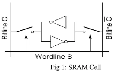
The memory circuit is claimed to be static if the hold on knowledge is maintained indefinitely, as long because the power provide is on, with none would like for periodic refresh operation. The information electric cell, i.e., the one-bit memory cell within the static RAM arrays, invariably consists of an easy latch circuit with 2 stable operative points. counting on the preserved state of the 2 electrical converter latch circuit, the information being command within the memory cell are going to be taken either as logic '0' or as logic '1'. To access the information contained within the memory cell via to a small degree line, we'd like a minimum of one switch, that is controlled by the corresponding word line as shown .
Fig 1: SRAM Cell
Available online: https://edupediapublications.org/journals/index.php/IJR/ P a g e | 1330 ability as contrasted and traditional 6TSRAM cell
.However, Writing1 through a nMOS pass transistor in 5T is an outline challenge. Another issue is to acquire advanced commotion edge against procedure variety sat all operations. What's more, the read soundness of single finished 5Tseverely corrupts in examination with customary 6T SRAM cell. Different methodologies like supported supply (entryway voltage of access transistor M5 is more prominent than VDD) produced from an extra circuit, gated-input compose help, 7T double VTH , asymmetrical write/read-help 8T , and cross-point information mindful 9T have been proposed to alleviate the above issues connected with 5T. Still, none of the cell could satisfy the prerequisite of enhancing both read and compose soundness in sub threshold administration for ultralow power applications.
In this brief, we have outlined another sub threshold 8T SRAM cell that works in sub nanometer innovation hub at ULV. This8T SRAM cell utilizes singlefinished compose with element criticism slicing to upgrade compose capacity and element read decoupling to dodge read disturb. Because of read decoupled system, the 9T cell improves the RSNM by 4.1× as contrasted and routine 6Tcell. The 9T cell has bigger composed edge (WT) as well as has faster composed time. As 8T is single-finished it can spare more power consumption and territory as contrasted. Here, we center mainly on the soundness of the cell which is influenced by the procedure parameter variations. This brief is a detailed dialog of our previous work on 8T, incorporating examinations with other single-finished cells like routine 5T and 8T.
We have additionally underscored on delay, force and half-select issues for both line and section. Aside from this, a 1-kb SRAM exhibit for proposed 8T and routine 6T was additionally planned. The circuit reproductions are done in
United Microelectronics Corporation (UMC) 90-nm process innovation at various force supplies.
II.EXISTING SYSTEM 6T SRAM CELL
Static random access memory (SRAM) can retain its stored information as long as power is supplied. This is in contrast to dynamic RAM (DRAM) where periodic refreshes are necessary or non-volatile memory where no power needs to be supplied for data retention, as for example flash memory. The term ``random access'' means that in an array of SRAM cells each cell can be read or written in any order, no matter which cell was last accessed.
The structure of a 6 transistor SRAM cell, storing one bit of information. The core of the cell is formed by two CMOS inverters, where the output potential of each inverter Vout is fed as input into the
other Vin. This feedback loop stabilizes the inverters
to their respective state.
The access transistors and the word and bit lines, WL and BL, are used to read and write from or to the cell. In standby mode the word line is low, turning the access transistors off. In this state the inverters are in complementary state. When the p-channel MOSFET of the left inverter is turned on,
the potential V1,out is high and the p-channel
MOSFET of inverter two is turned off, Vr,out is low.
Available online: https://edupediapublications.org/journals/index.php/IJR/ P a g e | 1331 To write information the data is imposed on
the bit line and the inverse data on the inverse bit
line, . Then the access transistors are turned on
by setting the word line to high. As the driver of the bit lines is much stronger it can assert the inverter transistors. As soon as the information is stored in the inverters, the access transistors can be turned off and the information in the inverter is preserved.For reading the word line is turned on to activate the access transistors while the information is sensed at the bit lines.
III.PROPOSED SYSTEM
To make a cell stable all told operations, single-ended with dynamic feedback control (SE-DFC) cell is bestowed in Fig. 3(a).
Fig.3 proposed 8T. (a) Schematic.
The single-ended style is employed to cut back the differential switch power throughout read– write operation. The ability consumed throughout switching/ toggling of knowledge on single bit line is lesser than that on differential bit-line try. The SE-DFC allows writing through single nMOS in 8T. It additionally separates the scan and write path and exhibits scan decoupling. The structural amendment
of cell is taken into account to reinforce the immunity against the process–voltage–temperature (PVT) variations.
It improves the static noise margin (SNM) of 8T cell in sub-threshold/near-threshold region. The projected 8T has one cross-coupled electrical converter try, within which every electrical converter is formed from 3 cascaded transistors. These 2 stacked cross-coupled inverters: M1–M2– M4 and M8–M6–M5 retain the information throughout hold mode. The write word line (WWL) controls only 1 nMOS semiconductor unit M7, accustomed transfer the information from single writes bit line (WBL). A separate read bit line (RBL) is employed to transfer the information from cell to the output once read word line (RWL) is activated. 2 columns biased feedback management signals: FCS1 and FCS2 lines are accustomed management the feedback cutting transistors: M6 and money supply, severally.
Write Operation
Available online: https://edupediapublications.org/journals/index.php/IJR/ P a g e | 1332 because the time taken by WWL signal-to-rise to
VDD/2 till the storage nodes encounter one another.
READ OPERATION
The read operation is performed by pre-charging the RBL and activating RWL. If one is keep at node letter of the alphabet then, M4 activates and makes a coffee resistive path for the flow of cell current through RBL to ground. This discharges RBL quickly to ground, which may be perceived by the total swing electrical converter sense electronic equipment. Since WWL, FCS1, and FCS2 were created low throughout the scan operation (Table II), therefore, there's no direct disturbance on true storing node QB throughout reading the cell. The low going FCS2 leaves QB floating, which matches to a negative worth then comes back to its original zero worth when eminent read operation. If Q is high then, the scale quantitative relation of M3 and M4 can govern the read current and therefore the voltage distinction on RBL. throughout read zero operation, Q is zero and RBL holds precharged high worth and therefore the electrical converter sense electronic equipment offers zero at output. Since money supply is OFF therefore virtual QB (VQB) is isolated from QB and this prevents the prospect of disturbance in QB node voltage that ultimately reduces the read failure chance and improves the RSNM. throughout scan operation, if FCS1/FCS2turns one before RWL is turned zero then QB and VQB will share charge. As WWL is zero no sturdy path exists between WBL and letter of the alphabet, and any disturbance in letter of the alphabet B won't have an effect on Q. afterward if RWL goes low, the feedback can restore the various states (Q=1andQB=0).
IV .EXPERIMENTAL RESULTS SCHEMATIC DESIGN :
The proposed 8t SRAM was designed using DSCH(Digital schematic) which is a backend tool. Below shown is a 8T SRAM cell.
LAYOUT DESIGN:
The layout for the designed schematic in DSCH can be obtained in a backend tool named MICROWIND. Below shown is a 8T SRAM Layout.
SIMULATION RESULT:
Available online: https://edupediapublications.org/journals/index.php/IJR/ P a g e | 1333
V.CONCLUSION
An 8T SRAM cell with high data stability that operates in ULV provides is given. we have a tendency to earned increased SNM in sub threshold regime exploitation SE-DFC and skim decoupling schemes. The projected cell’s space is doubly as that of 6T. Still, it’s higher integral method tolerance and dynamic voltage relevancy allows it to use just like cells (8T, 9T, and one0T) at the side of 1.8×−2×area overhead. The projected 8T cell has high stability and might be operated at ULV of 200– 300 mV power provides. The advantage of reduced power consumption of the projected 8T cell allows it to use for battery operated SoC style. Future and applications of the projected 8T cell will probably be in low/ULV and radio frequency operation like neural signal processor, sub threshold processor, wide-operating-range IA-32 processor, quick Fourier remodel core, and low voltage cache operation. The projected system consumes terribly less power than that of existing SRAM cell.
REFERENCES
[1] K. Roy and S. Prasad, Low-Power CMOS VLSI Circuit Design,1sted. New York, NY, USA: Wiley, 2000.
[2] N. Verma and A. P. Chandrakasan, “A 256 kb 65 nm 8T subthreshold SRAM employing
sense-amplifier redundancy,” IEEE J. Solid-State Circuits, vol. 43, no. 1, pp. 141–149, Jan. 2008.
[3] C. Kushwah and S. K. Vishvakarma, “Ultra-low power sub-threshold SRAM cell design to improve read static noise margin,” inProgress in VLSI Design and Test(Lecture Notes in Computer Science), vol. 7373. Berlin, Germany: Springer-Verlag, 2012, pp. 139–146.