DESIGN, ANALYSIS AND SIMULATION OF TRIPLE
BAND EQUAL SPLIT WILKINSON POWER DIVIDER
WITH IMPROVE RETURN LOSS AND BANDWIDTH
ON MICROSTRIP LINE
Santosh kumar
1, Gaurav Saxena
2, Ishrat Jamal nasir
31,3
Department of Electronics& Comm. Engineering, MDU, Rohtak, (India)
2
Department of Electronics& Comm. Engineering, Galgotia University, G.Noida,( India)
ABSTRACT
With The Rapid Development in wireless/wire line communications, functions of Power Dividers are
enhanced and their applications are used in the field of Radio technology. . Among various RF passive
circuits, Wilkinson power divider is a basic and important component in application to RF power
amplifiers, mixers, phased-array antennas, and many kinds of equipment. Equal Split Wilkinson Power
Divider is also known as 3 dB power Divider. The Wilkinson power divider is a well-known device in the
RF/microwave community used for splitting or combining signals. It is composed of simple transmission
lines and a resistor, and takes advantage of the properties of quarter- wavelength transmission line sections
to provide Ideal power divider characteristics. A circuit analysis of the general Wilkinson power divider
schematic is performed to provide insight into the device characteristics as well as present a clear
derivation of the correlating scattering matrix. A thorough comparison between the performances of each of
the different designs is conducted and the results are provided and discussed. In this project our aim is to
improve the specifications of Equal Split Power Divider by: Isolation Loss (> 40 dB), Return Loss and Equal
Power Bandwidth.
Keywords: Dual Band Wilkinson Power Divider, Even Odd Mode Analysis, Microstrip Patch
Antenna, S-Parameters S12 S13 S21 and S31, Triple band Wilkinson Power Divider.
I INTRODUCTION
Different techniques are used to modify and simulate the Wilkinson Power Divider .The Wilkinson
Power Divider at two different frequencies is presented. The structure of this power divider and the
formula used to determine the design parameters have been given. The circuits also feature a simple
structure with realistic impedance values and distributed design with reduced parasitic effects (in
compared with lumped elements) and exact solution (ideal characteristics). All the structure is presented
for the dual band operation. A structure is also given in which the divider has two output ports shifted
away from the isolation resistor to the middle of the divider and an open stub at the input port. A new
scheme is also proposed for dual band operation. The dual band operation is achieved by attaching
two central transmission line stubs to the conventional Wilkinson Power Divider.
II DESIGN SPECIFICATIONS
Software used in this project is Circuit Simulator Microwave Office2002.
1.
Desired frequency = 1 GHz to 5 GHz2.
Source Impedance = 50 ohm.
3.
Load Impedance = 50 ohm.4.
Substrate Permittivity = 2.16 (RT Duroid 5880) , 12.9 (GaAs), 3.38(Isola)5.
Height of substrate = 1.524 µm.6.
Thickness of Conductor = 0.001 µm.The three essential parameters for the design of a rectangular Microstrip Patch Antenna are:
Frequency of operation ( fo ): The resonant frequency of the antenna must be selected appropriately.
For Uplink and Downlink in Satellite Communication uses the frequency range in GHz. Hence the Power
divider designed must be able to operate in this frequency range. The resonant frequency selected for
my design is 1GHz to 5 GHz.
Dielectric constant of the substrate (ϵr): The dielectric material selected for my design is RT Duroid,
GaAs and Isola. A substrate with a high dielectric constant has been selected since it reduces the
dimensions of the substrate.
Height of dielectric substrate (h): For the substrate to be used in device, it is essential that the power
divider is not bulky. Hence, the height of the dielectric substrate is selected as 1.524 µm. It varies
according to the impedance required and their electrical length.
III SIMULATION SETUP
The software used to model and simulate Wilkinson Power Divider is Microwave office2002 software. Microwave
Office is a full-wave electromagnetic simulator. This is the AWR (Applied Wave Research) software for
designing Microwave Integrated Circuits It analyzes 3D and multilayer structures of general shapes of Microstrip
Line. It has been widely used in the design of MICs, RFICs, patch antennas, wire antennas, and other RF/wireless
antennas. It can be used to calculate and plot the S11 parameters, VSWR, bandwidth, return loss as well as the
radiation patterns. An evaluation version of the software was used to obtain the results.
IV GRAPHICAL ANALYSIS
We have seen the schematic circuits of Wilkinson Power Divider. Their analysis is given below. Final and
the best result is given in the last .All have different substrate permittivity. From the graph, return loss,
V FIGURES AND TABLES
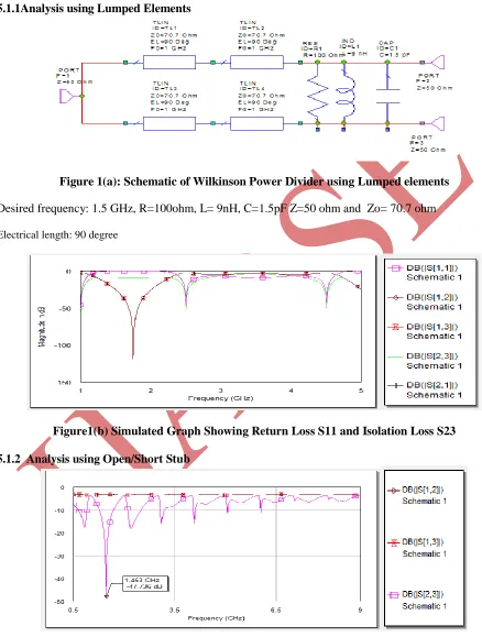
5.1.1Analysis using Lumped Elements
Figure 1(a): Schematic of Wilkinson Power Divider using Lumped elements
Desired frequency: 1.5 GHz, R=100ohm, L= 9nH, C=1.5pF Z=50 ohm and Zo= 70.7 ohm
Electrical length: 90 degree
Figure1(b) Simulated Graph Showing Return Loss S11 and Isolation Loss S23
5.1.2 Analysis using Open/Short Stub
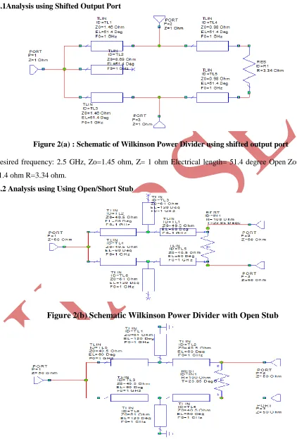
5.2.1Analysis using Shifted Output Port
Figure 2(a) : Schematic of Wilkinson Power Divider using shifted output port
Desired frequency: 2.5 GHz, Zo=1.45 ohm, Z= 1 ohm Electrical length= 51.4 degree Open Zo=
51.4 ohm R=3.34 ohm.
5.2.2 Analysis using Using Open/Short Stub
Figure 2(b) Schematic Wilkinson Power Divider with Open Stub
Desired Frequency =1.3 GHz
Electrical length= 60 degree for Z=40.5 ohm
Electrical length =120 degree for Z= 61 ohm
At ports Z=50 ohm R=100 ohm
Open At between Circuits
Desired Frequency= 1.8 GHz
At ports Z = 50 ohm
Electrical length= 60 degree for Z=40.5 ohm
Electrical length =120 degree for Z= 61 ohm
At ports Z=50 ohm R=100 ohm
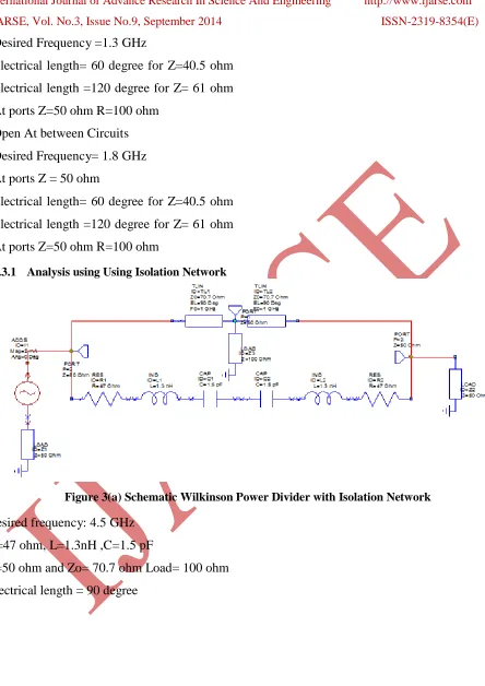
5.3.1
Analysis using Using Isolation Network
Figure 3(a) Schematic Wilkinson Power Divider with Isolation Network
Desired frequency: 4.5 GHz
R=47 ohm, L=1.3nH ,C=1.5 pF
Z=50 ohm and Zo= 70.7 ohm Load= 100 ohm
Figure 3(b) Simulation Graph
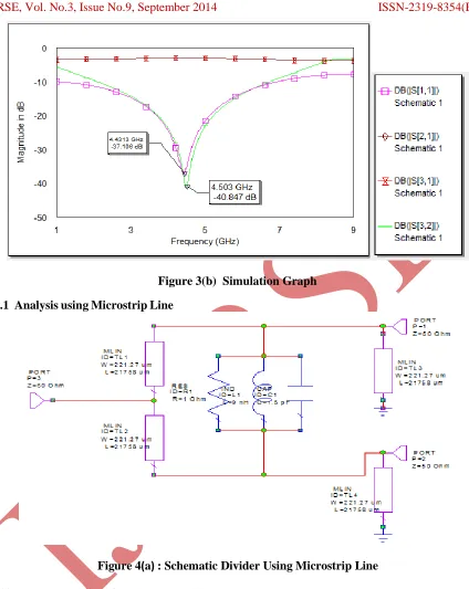
5.4.1 Analysis using Microstrip Line
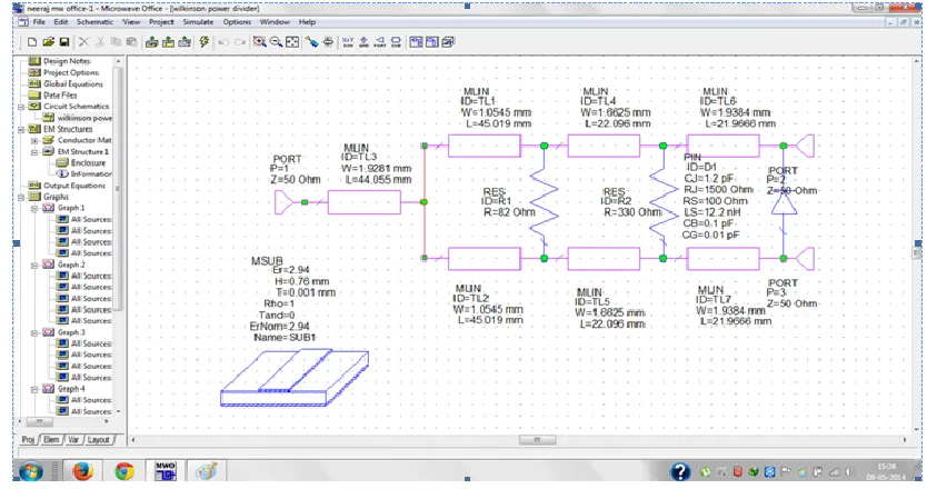
Figure 4
(
a
)
: Schematic Divider Using Microstrip Line
Wilkinson Power Desired frequency = 4.8 GHz ,
Figure 4(b) Schematic Wilkinson Power Divider using T junction with Microstrip Line
VI FINAL RESULT
As per the different analysis shown above the best result is modified. This result shows the maximum
return loss and a good Equal Power Bandwidth. Here the desired frequency is f1=0.9 GHz, f2=3.4GHz
& f3=5.45 GHz. The schematic Wilkinson power divider and their desired graph are shown below.
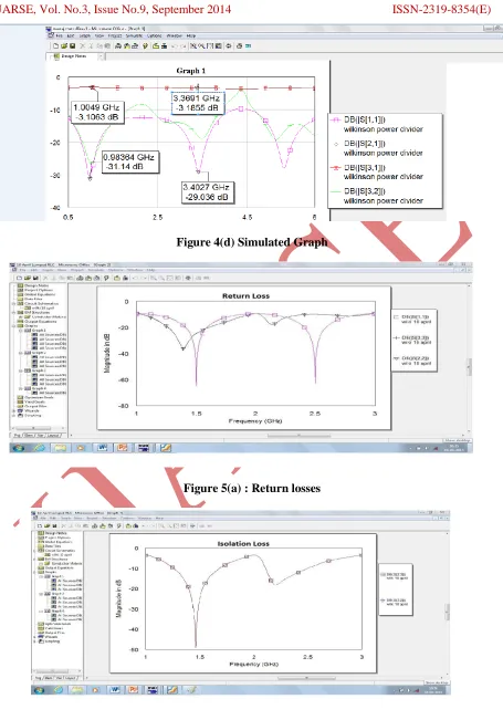
Figure 4(d) Simulated Graph
Figure 5(a) : Return losses
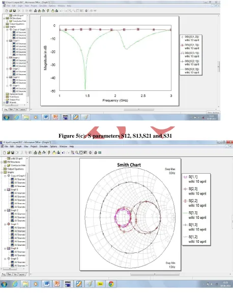
Figure 5(c): S parameters S12, S13,S21 and S31
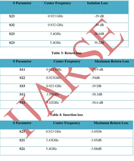
Values of S parameters are given in Table 2 and Table 3:
Table 2: Isolation Loss
S Parameter
Center Frequency
Isolation Loss
S23
0.923 GHz
-39 dB
S32
0.932 GHz
-39 dB
S23
3.4GHz
38.9dB
S23
5.4GHz
39.2dB
Table 3: Return loss
S Parameter
Center Frequency
Maximum Return Loss
S11
0.923 GHz
-38.9 dB
S22
0.923GHz
-39dB
S33
0.923 GHz
-39 DB
S11
3.43GHz
-38.3dB
S11
5.42GHz
-38.6 dB
Table 4: Insertion loss
S Parameter
Center Frequency
Maximum Return Loss
S21
0.923 GHz
-3.05Db
S21
3.43GHz
-3.05dB
S21
5.4GHz
-3.08dB
VII CONCLUSION
can achieve very similar results when constructed using Lumped elements at reasonable frequencies (< 1GHz).
The schematic of equal split Wilkinson power divider was drawn and the layout was generated. The results
of the project were in agreement to the theoretical available results, so the various S parameters were plotted
as shown above.
In this project we conclude that the isolation loss of equal Split Power Divider has been achieved. The return
loss and isolation loss for a UWB T r i p l e b a n d Wilkinson Power Divider is -38.2 dB and -39.6 dB
respectively. Equal Power Bandwidth is around 4.5 GHz. Analysis is done on the desired frequency of 1.5
GHz at Z0 = 50 ohm. It has been designed for f1=0.93GHz, f2= 3.43 GHz & f3=5.42GHz.
VIII FUTURE WORK
With The Rapid Development in wireless/wire line communications, functions of Power Dividers are enhanced
and their applications are used in the field of Radio technology. In satellite communication and also in
Military applications it can be widely used. Its quarter wavelength can provide maximum power transfer .For
industrial systems power combiner/ splitter is very useful for dividing the powers equally. In Wireless
communication uplink and downlink at desired frequencies this device is beneficial.
REFERENCES
[1]. D. Pozar, Microwave Engineering, 3rd ed. Hoboken, New Jersey: John Wiley & Sons Inc. pp. 308-361,
2005.
[2]. Xiaolong Wang,Iwata Sakagami, Kensaku Takahashi ,Shingo Okumura,” A Generalized Dual Band
Wilkinson Power Divider With Parallel L,C and R Components”IEEE Transactions on Microwave
Theory and Techniques, Vol.60 no.4,April 2012.
[3]. Lei Wu,Zengguang Sun HayyatinYilmaz and Manfred Berroth,”A Dual Frequency Wilkinson Power
Divider”IEEE Transactions on Microwave Theory and Techniques,Vol.54,no.1,January 2006.
[4]. Myun Joo and Byungje Lee,” A Dual Band Wilkinson Power Divider” IEEE Microwave and
Wireless Components Letter, Vol.18,no.2 February 2008.
[5]. Jui-Chih,,Zuo-MinTsai,Kun-Yu and Huei Wang,”A Modified Wilkinson Power Divider With
Isolation Bandwidth Improvenment”, IEEE Transactions on Microwave Theory and
Techniques,Vol.60,no.9,Sept 2012
[6]. Kwok-Keung,M.Cheng and Fai Leung,” A New Wilkinson Power Divider Design for Dual Band
Application,” IEEE Microwave and Wireless Components LettersVol.17,no.9,September 2007.
[7]. Sung Hwan, J.W.Lee ,Choon Sik Cho,” A Wilkinson Power Divider With Different Power Ratios at