On-chip temperature-based digital signal processing for
customized wireless microcontroller
Siti Farhah Razanah Faezal1, *, Mohd Nazrin Md Isa1, Azizi Harun1, Shaiful Nizam Mohyar1, and Asral Bahari Jambek1
1School of Microelectronic Engineering, Universiti Malaysia Perlis, 02600 Malaysia.
Abstract. Increases in die size and power density inside system-on-chip (SoC) design have brought thermal issue inside the system. Uneven heat-up and increasing in temperature offset on-chip has become a major factor that can limits the system performance. This paper presents the design and simulation of a temperature-based digital signal processing for modern system-on-chip design using the Verilog HDL. This design yields continuous monitoring of temperature and reacts to specified conditions. The simulation of the system has been done on Altera Quartus Software v. 14. With system above, microcontroller can achieve nominal power dissipation and operation is within the temperature range due to the incorporate of an
interrupt-based system.
1 Introduction
The measurement of temperature is very critical especially in portable devices with densely packed circuits which can dissipate power in the form of heat. The continuous increase of the operating frequency increases the density of dissipated power [1]. As power consumption, P is directly proportional to the operational frequency, f by the following equation:
P = c. V2 . f + Ps (1)
where c is scaling constant with the dimension of capacitance (F). V is an input voltage and Ps is the static power dissipation which is the power at a zero clock frequency [2]. Rise in heat density creating vast difficulties which lead to serious thermal problem even though in low power applications.
Thermal considerations should become one of the important part of the electrical design process. To increase system reliability, the temperature of the operating circuits should be continuously watched during the operation of system [3]. Local overheating in one spot of a density circuit as in Fig.1, such as high-speed mixed-signal circuits, can cause a whole system to crash due to clock synchronization problems, parameter mismatches or other coefficient changes due to the uneven heat-up on a single chip [3].
Heat sinks and fans, known as passive heat dissipation mechanisms, are widely used in system design. Advanced circuit designs recently have included active mechanisms that detect and handle an over-heating even
[4]. The improvement in cooling technology are quite slow. In the mobile system and external skin hot spots, the implemented cooling fan can be a major source of acoustic noise [5].
Fig. 1. Die hotspot of high density circuit [5].
Interface (ACPI), thermal management in personal computer systems [6]. ACPI is an industry standard infrastructure that facilitate thermal management of computer platforms. Thermal management is done by the use of active cooling devices, such as fans, or passive cooling actions. However, the ACPI standard is quite limited, as it simply supports extra control to turn on or off a cooling mechanism and shift the alert level, which is feedback to the system [7]. Meanwhile, later, Dynamic Frequency Voltage Scaling (DVS) is proposed [8]. These mechanisms were implemented in CPUs such as the Intel® Centrino® Processor [9]. Thus, the important feedback required for power and thermal management systems is temperature measurement and monitoring.
Increases in die size and power density inside system-on-chip (SoC) design have brought thermal issue inside the system. Uneven heat-up and increasing in temperature offset on-chip has become a major factor that can limits the system performance [10]. In order to meet this challenge, we proposed a system that is temperature-aware system that is able to monitor the temperature distributions on-chip without any knowledge about the material properties or the chip structure.
In this project, we are developing a temperature-based digital signal processing IP circuit (TDSP). Moreover, this research covers Verilog HDL and design of a temperature-based digital signal processing module for an on-chip temperature monitoring system using Altera Quartus software. This circuit is optimized in architecture and circuit implementation to fit system-on-chip designs. Therefore, an interrupt-based system will be implemented.
2
Proposed Architecture
2.1. Circuit Blocks
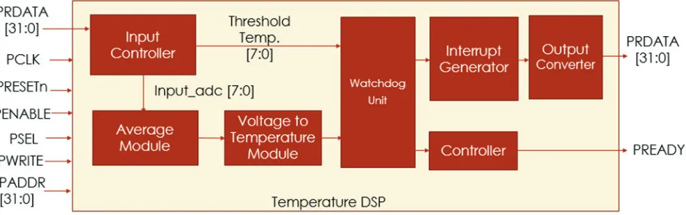
The block diagram of the temperature-based digital signal processing circuit is shown in Fig. 2. The function of every block is describe in Section 2.2.
Fig. 2. Temperature-based DSP circuit block diagram
2.2 Function
Function of each block is describe in details in this section;
• Input Controller: This unit used to control the input data received and providing an input interface synchronously.
• Average Module: This unit contains five registers to store the data received from ADC and provided average data output.
• Voltage to Temperature Module: This unit contains a look-up table to convert the input ADC which is in voltage value into the corresponding temperature value in Celsius (˚C).
• Parameterizable Watchdog Unit: This unit contains two monitoring circuits: the threshold monitor for each temperature sensor, and the offset temperature monitor. Both circuit providing sufficient speed to compare temperature provided in the system.
• Interrupt Generator: This unit provides data outputs that are read by the system CPU, like temperature value, offset temperature value, and interrupt types.
• Output Converter: This unit convert the output into [31:0] bit form (including temperature threshold, interrupt).
• Controller: This unit control the interaction between the system and CPU.
3 Flowchart of The System
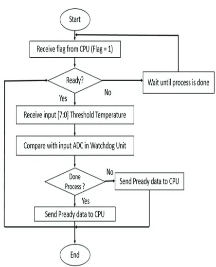
Consider the flowchart in Fig.3 below is indicating the process flow for temperature-based digital signal processing.
Fig. 3. Flowchart of the TDSP system
When the system is ready, the input controller would receive an input from ADC in 8-bit binary form of voltage value. After received in total of 5 different input, average module will automatically calculate the average value of the inputs and generate the average output.
Then, simultaneously, voltage to temperature module would process the input received and generated an output equivalent to temperature in degree Celsius (˚C). Parameterizable watchdog unit would monitor the threshold temperature (if available) as in flowchart Fig. 4 below and offset temperature and send signals to the interrupt and output generator.
Interrupt is produced when the temperature is very lower (-25˚C - 0˚C) and also when the temperature is very high (61˚C - 80˚C). Output converter will then convert all information (including temperature value, offset temperature value, and interrupt types) into output [31:0]
Fig. 4. Flowchart of the TDSP system when threshold temperature is available.
3 Architecture on APB Bus
The temperature sensor ranges from -25˚C to 80˚C and convert it into equivalent 1.38mV/˚C. This analog voltage gets converted into equivalent 8-bit digital voltage through ADC. These 8-bit inputs are applied to TDSP where TDSP will monitor the threshold and offset temperature inside the system and implement the interrupt-based system if the condition needed. The programming in TDSP is done by Verilog HDL language and that builds TDSP system module. The block diagram for architecture on APB:
5 Simulation Result
Fig. 6. RTL Level Synthesis of TDSP System
The ALTERA QUARTUS software generates the output waveform corresponding to input change of ADC or threshold temperature on simulation. This simulation is executed by random values chosen in inputs. RTL level synthesis of simulation is generated by QUARTUS software after code is compiled. The RTL level synthesis is the lowest level representation of circuitry from QUARTUS software. The RTL generated for TDSP is shown in Fig. 6 above.
6 FPGA Implementation
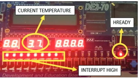
TDSP system is implemented using DE2-70 Altera Board to check the flexibility and functionality of the system. DE2-70 is used due to its capability to be used in wide range of experiments development of the FPGA-based systems, as well as design of hardware controllers. Altera DE2 board is connected the PC using USB-blaster provided with DE2 package. Fig.7 & Fig. 8 below shows the result on FPGA Board.
Fig.7. Result when temperature exceeding threshold
temperature
Fig.8. Result when temperature lower than threshold
temperature
7 Conclusion and Future Work
This work is supported in part by Talentcorp Malaysia grant also collaborated with Intel Malaysia and CEDEC USM for 3D (Demand, Driven, Develop) program. I would also like to thank to my supervisor, Dr. Mohd Nazrin Bin Mohd Isa, and my 3D teammates, Azwan, Zhafirah and Wang Hang Suan for being so helpful throughout this project. And lastly, special thanks goes to my family members for their outstanding supports.
References
1. M. Szermer, Z. Kulesza, M. Janicki, and A. Napieralski, 3, pp. 529–532 (2008)
2. N.H.E Weste, D.M. Harris, CMOS VLSI Design A Circuits and System Perspective, 4th ed. (Addison Wesley, 2011)
3. V. Szekely, M. Rencz, and B. Courtois, Proc. 13th IEEE SEMITHERM Symposium, pp. 210– 217 (1997)
4. J. Draper, J. Block, J. Koller, and C. Steele, Proc. Lecture Notes in Computer Science 1388 (IPPS/SPDP’98 Workshops Proceedings), pp. 900–901 (1998)
5. E. Rotem and M. Platform, Temperature measurement in the Intel ® Core TM Duo Processor, pp. 1–5.
6. Compaq, Intel, Microsoft, Phoenix, and Toshiba, Advanced configuration and power interface specification (2000)
7. J. Steele, Proc. Wescon 98, pp. 169–182 (1998) 8. D. Brooks, M. Martonosi, Proceedings of the
HPCA-07 (2001)
9. http://download.intel.com/design/mobile/datash ts/30218908.pdf
![Fig. 1. Die hotspot of high density circuit [5].](https://thumb-us.123doks.com/thumbv2/123dok_us/8125319.1353907/1.595.312.533.442.690/fig-die-hotspot-high-density-circuit.webp)