Fast Calculation Using Vedic Multiplier with Different Algorithms and
High Performance
Ravitesh Mishra, Professor, DEPARTMENT OF ELECTRONICS AND COMMUNICATION ENGINEERING
UNIVERSITY INSTITUTE OF TECHNOLOGY, AISECT UNIVERSITY, BHOPAL, MADHYA PRADESH, INDIA
Ashish Chouhan, Professor, Head-of-Department, DEPARTMENT OF ELECTRONICS AND
COMMUNICATION ENGINEERING UNIVERSITY INSTITUTE OF TECHNOLOGY, AISECT UNIVERSITY,
BHOPAL, MADHYA PRADESH, INDIA
Pratibha Singh, DEPARTMENT OF ELECTRONICS AND COMMUNICATION ENGINEERING UNIVERSITY
INSTITUTE OF TECHNOLOGY, AISECT UNIVERSITY, BHOPAL, MADHYA PRADESH, INDIA
Abstract:
A high speed and low power 16×16 Vedic Multiplier is designed by using low power and high speed changed carry choose adder. This work proposes a high speed Vedic Multiplier primarily based on area, delay and power efficient Carry Choose Adder. In this paper a quick methodology of multiplication based on ancient Indian Vedic arithmetic is proposed. The whole of Vedic arithmetic is based on 16 sutras and manifests a unified structure of arithmetic. Among the varied ways of multiplication in Vedic arithmetic, Urdhava tiryakbhyam is discussed intimately. All the redundant logic operations present in the traditional CSLA are eliminated and proposed a brand new logic formulation for CSLA. The proposed CSLA design involves considerably less space and delay than the recently proposed BEC-based CSLA. The multiplier mentioned here is compared with other multiplier to spotlight the speed and power superiority of the vedic multiplier.
Index Terms:
Carry Select Adder, Logic formulation, Vedic Multiplier.
I.NTRODUCTION:
Multiplication is one of the elemental block in almost all the arithmetic logic units. This Vedic multiplication is mainly utilized in the fields of the Digital Signal Processing (DSP) and also in so several applications like Fast Fourier Transform, convolution, filtering and microprocessor applications [2,3,9]. In most of the DSP algorithms multiplier is one of the key part and hence a high speed and area economical multiplier is required and multiplication time is additionally one of the predominant factor for DSP algorithms. The ancient mathematical techniques like Vedic mathematics used to cut back the computational time such that it can increase speed and conjointly require less hardware.
mathematics mainly consists of the sixteen sutras which it will be related to the different branches of arithmetic like algebra, arithmetic geometry.
II. ANCIENT VEDIC MATHEMATICAL
ALGORITHMS:
The Vedic mathematics mainly reduces the advanced typical calculations in to simpler by applying sutras as stated above. These Vedic mathematic techniques are very efficient and take very less hardware to implement. These sutras are mainly used for multiplication of two decimal numbers and we extend these sutras for binary multiplications. Some of the techniques are discussed below:
A.
Urdhva -Tiryakbhyam Sutra
(Vertically and Crosswise):
Booth multipliers are generally used for multiplication purposes. Booth Encoder, Wallace Tree, Binary Adders and Partial Product Generator are the main elements used for Booth multiplier architecture. Booth multiplier is mainly used for two applications are to extend the speed by reduction of the partial products and additionally by the way that the partial products to be added. In this section we tend to propose a Vedic multiplication technique referred to as “Urdhva-Tiryakbhyam - Vertically and crosswise,” which will be used not only for decimal multiplication however conjointly used for binary multiplication as well. This technique mainly consists of generation of partial merchandise parallel and then we should perform the addition operation simultaneously [3]. This algorithm will be used for 2x2, 4x4,
8x8....N×N bit multiplications. Since the sums and their partial products are calculated in parallel the Vedic multiplier will not depends upon the processor clock frequency.[1]
Hence there is no need of sky-rocketing the clock frequency and if the clock frequency will increase it can automatically results in the increase in the ability dissipation. Hence by using this Vedic multiplier technique we have a tendency to reduce the ability dissipation. The foremost advantage of this Vedic multiplier is that it can reduce delay plus space compared with the other multipliers.
B.
Example for Decimal Multiplication
Using Vedic Mathematics:
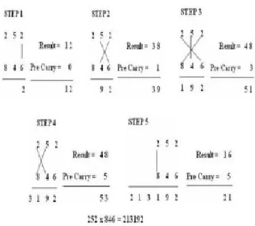
Figure 1. Multiplication of two decimal numbers
III. MODIFIED VEDIC MULTIPLIER ARCHITECTURE:
The architectures for 2×2, 4×4, 8×8, 16×16. . .N×N bit modules are mentioned in this section. During this section, the technique used is 'Urdhva-Tiryakbhyam' (Vertically and Crosswise) sutra that could be a straightforward technique for multiplication with lesser range of steps and conjointly in very less computational time. The main advantage of this Vedic multiplier is that we can calculate the partial merchandise and summation to be done concurrently. Hence we tend to using this Vedic multiplier in nearly all the ALU's.
A.
2×2 Vedic Multiplier Block:
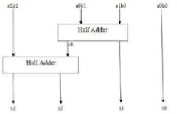
To explain this method let us consider 2 numbers with 2 bits each and the numbers are A and B where A=a0a1 and B=b0b1 as shown in the below line diagram. First the least significant bit (LSB) bit of final product (vertical) is obtained by taking the product of two least significant bit (LSB) bits of A and B is a0b0.
Second step is to take the products in a crosswise manner such as the least significant bit (LSB) of the first number A (multiplicand) is multiplied with the next higher bit of the multiplicand B in a crosswise manner. The output generated is 1-Carry bit and 1bit used in the result as shown below. [7]Next step is to take product of 2 most significant bits (MSB) and for the obtained result previously obtained carry should be added. The result obtained is used as the fourth bit of the final result and final carry is the other bit.
s0 = a0b0 (1) c1s1 = a1b0 + a0b1 (2) c2 s2 = c1 + a1b1 (3)
Figure 2. Block Diagram of 2×2 Vedic Multiplier
B.
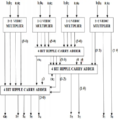
4x4 Vedic Multiplier Block:
In this section, now we will discuss about 4x4 bit Vedic multiplier. For explaining this multiplier let us consider two four bit numbers as A and B such that the individual bits can be represented as the A3A2A1A0 and B3B2B1B0. The procedure for multiplication can be explained in terms of line diagram shown in below figure. The final output can be obtained as the C6S6S5S4S3S2S1S0.
The partial merchandise are calculated in parallel and hence delay obtained is decreased enormously for the increase in the amount of bits. The Least Significant Bit (LSB) S0 is obtained simply by multiplying the LSBs of the multiplier and also the multiplicand. Here the multiplication is followed as per the steps shown in the line diagram in figure 3. After performing all the steps the result (Sn) and Carry(Cn) is obtained and in the same way at every step the previous stage carry is forwarded to a higher stage and the process goes on. [4] S0 = A0B0 (4) C1S1 = A1B0 + A0B1 (5)
Figure 3. Block Diagram of 4x4 bit Vedic Multiplier
C.
8x8 Vedic Multiplier Block:
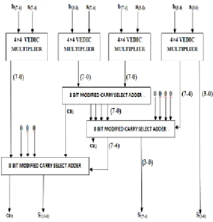
In this section, currently we have a tendency to discuss regarding 4x4 bit Vedic multiplier. For explaining this multiplier let us consider 2 eight bit numbers as A and B such that the individual bits will be represented as the A7A6A5A4A3A2A1A0 and B7B6B5B4B3B2B1B0. The procedure for multiplication will be explained in terms of line diagram shown in below figure 4. The final output can be obtained
as the
16S15S14S13S12S11S10S9S8S7S6S5S4S3S2S1S0 . The partial merchandise are calculated in
Figure 4. Block Diagram of 8x8 bit Vedic Multiplier For clear understanding, observe the block
diagrams for 8x8 as shown below and among the block diagram 8x8, in total there are four 4x4 Vedic multiplier modules, and three modified carry choose adders of 8 bit size are used. The 8 bit modified carry choose adders are used for addition of two eight bits and likewise totally four are use at intermediate stages of multiplier. The carry generated from the primary modified carry select adder is passed on to the next changed carry choose adder and there are four zero inputs for second changed carry choose adders. The arrangement of the modified carry select adders are shown in the block diagram which will reduce the computational time so that the delay will be decrease.
D.
16x16 Vedic Multiplier Block:
In this section, now we tend to discuss concerning to 4x4 bit Vedic multiplier [10]. For
explaining this multiplier allow us to take into account two 16 bit numbers as A and B such that the individual bits will be represented because the A [15:0] and B [15:0]. The procedure for multiplication will be explained in terms of line diagram shown below in figure 5. The final output can be obtained as the C16S[31:0]. The partial products are calculated in parallel and hence delay obtained is decreased enormously for the rise in the quantity of bits. The Least Significant Bit (LSB) S0 is obtained easily by multiplying the LSBs of the multiplier and therefore the multiplicand. Here the multiplication is followed according to the steps shown in the line diagram in figure. After performing all the steps the result (Sn) and carry (Cn) is obtained and in the same manner at each step the previous stage carry is forwarded to the next stage and the process goes on.
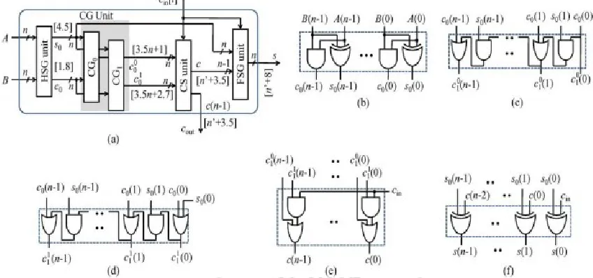
The CSLA has two units: 1) the sum and carry generator unit (SCG) and 2) the sum and carry selection unit as shown in the figure 5. The SCG unit consumes most of the logic resources of CSLA and significantly contributes to the critical path. Different logic designs have been suggested for efficient implementation of the SCG unit. We made a study of the logic designs
suggested for the SCG unit of conventional and BEC-based CSLAs of by suitable logic expressions. The main objective of this study is to identify redundant logic operations and data dependence. Accordingly, we remove all redundant logic operations and sequence logic operations based on their data dependence.
Figure 5. Structure of the BEC-based CSLA; n is the input operand bit-width The proposed CSLA is based on the logic
formulation as and its structure is shown in Figure 6(a). It consists of one HSG unit, one FSG unit, one CG unit, and one CS unit. The CG unit is composed of two CGs (CG0 and CG1) corresponding to input-carry “0” and “1”. The HSG receives two n-bit operands (A and B) and generate half-sum word S0 and half-carry word C0 of width n bits each. Both CG0 and CG1 receive S0 and C0 from the HSG unit and generate two n-bit full-carry words C11 and C10 corresponding to input-carry “0” and “1”, respectively. The logic diagram of the HSG unit is shown in Figure 6(b). The logic circuits of CG0 and CG1 are optimized to take advantage of the
fixed input-carry bits. The optimized designs of CG0 and CG1 are shown in Figure 6(c) and (d), respectively.
S0(i) = A(i) (+) B(i),C0(i) = A(i) . B(i) (11)
C10(i) = C10(i-1) . S0(i) + C0(i) for (10(0) = 0) (12)
C11(i) = C11(i-1) . S0(i) + C0(i) for (11(0) = 1) (13)
carry words c10 and c11 follow a specific bit pattern. If c01(i)= 1, then c11(i)=1,irrespective of s0(i) and c(i), for 0 = i = n - 1. This feature is used for logic optimization of the CS unit. Optimized design of the CS unit is shown in Figure 6(e), which is composed of n AND–OR gates. The final carry word C is obtained from the CS unit. The MSB of C is sent to output as Cout and (n-1) LSBs are XORed with (n - 1) MSBs of half-sum (S0) In the FSG [shown in Figure 6(f)] to obtain (n - 1) MSBs of final-sum(s) .The LSB of S0 is XORed with Cin to obtain the LSB of
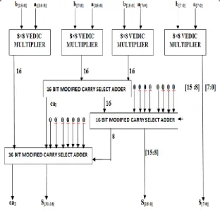
S. The architecture of 16x16 Vedic multiplier using “Urdhva Tiryagbhyam” Sutra is shown in Figure7. The 16x16 Vedic multiplier architecture is implemented using four 8x8 Vedic multiplier modules, three 16 bit modified carry select adder.The first step in the design of 16×16 block will be grouping the 8 bit of each 16 bit input. [6]These pair terms will form vertical and crosswise product terms. Each input bit-pair is handled by a separate 8×8 Vedic the schematic of a 16×16 block designed using 8×8 blocks. The partial products represent the Urdhva vertical and cross product terms.
Figure 6. (a) Proposed CS adder design, where n is the input operand bit-width.(b) Gate-level
design of the HSG. (c) Gate level optimized design for input-carry =0. (d) Gate-level optimized design for input-carry =1. (e) Gate-level design of the CS unit. (f) Gate-Gate-level design
of the final-sum generation (FSG) unit.
Optimized design of the CS unit is shown in Fig. 6(e), which is composed of n AND–OR gates. The final carry word C is obtained from the CS unit. The MSB of C is sent to output as Cout and
Figure 7 (b). Logic Diagram of 16x16 bit Vedic Multiplier.
IV. RESULTS AND COMPARISON:
In 2×2, 4×4, 8×8, 16×16 multiplication operations were designed using Verilog HDL and simulation is performed in Xilinx; RTL compilation is performed in RC and physical design is carried out using Encounter RTL Compiler under Cadence environment as shown in Figure 9.
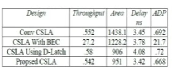
We have coded the Vedic Multiplier in VHDL using the proposed CSLA design and the existing CSLA designs for bit-widths 8, 16, and 32. All the designs are synthesized in the Cadence Design Suit. The net list file obtained from the DC are processed in the IC Compiler (ICC). After placement and route, the area, Delay, and power reported by the ICC are listed Table 1 for comparison. As shown in Table 1, the proposed SQRT-CSLA involves significantly less area and
less delay and consumes less power than the existing designs. We can find from Figure 8 that the proposed Multiplier design offers a saving of 39% ADP and 37% energy than the conventional Vedic Multiplier; The proposed CSLA saves 32% ADP and 33% energy than the BEC-based SQRT-CSLA; on average, for different bit-widths.
The proposed system was analyzed for performance and overhead with existing multiplication techniques. The result of performance analysis is visualized in the form of graph to provide a clear insight on the improvements achieved. This analysis was carried out on the following metrics: throughput, Area, ADP, and speed. The resultant value is tabulated.
Table 1: Parameter measurements
Figure 8. Performance analysis of proposed system v/s existing systems.
Figure 9. Simulation Result The values and the graph proves that this
system is more efficient than any existing location calibration techniques based on the ground of fairness, adaptability, scalability and minimal cost for communication and calibration and has minimal computational overhead.
V.CONCLUSION :
This entire work relies on making an area, delay and power efficient Vedic multiplier based on carry choose adder. This paper presents a unique way of realizing a high speed multiplier
15.050 ns which is less when put next to the whole delay of any different renowned multiplier architecture. Results also indicate a 13.65pc increase in the speed in comparison to traditional Vedic multiplier without carry choose adder technique..
REFERENCES :
[1] Aniruddha Kanhe, Shishir Kumar Das and Ankit Kumar Singh, “Design and Implementation of Low Power Multiplier Using Vedic Multiplication Technique”, (IJCSC) International Journal of Computer Science and Communication Vol. 3, No. 1, January-June 2012, pp. 131-132
[2] H. Thapliyal and H.R Arbania. “A Time-Area-Power Efficient Multiplier and Square Architecture Based On Ancient Indian Vedic Mathematics”, Proceedings of the 2004, International Conference on VLSI (VLSI’04), Las Vegas, Nevada, June 2004, pp. 434-9.
[3] Himanshu Thapliyal and M.B.Srinivas, “VLSI Implementation of RSA Encryption System Using Ancient Indian Vedic Mathematics”, Center for VLSI and Embedded System Technologies, International Institute of Information Technology Hyderabad-500019, India.
[4] S. Hong, S. Kim, M.C. Papaefthymiou, and W.E.Stark, .Low power parallel multiplier design for DSP applications through coefficient optimization, in Proc. of Twelfth Annual IEEE Int. ASIC/SOConf. Sep.1999, pp. 286-290. [5] R. Pushpangadan, V. Sukumaran, R.Innocent, D. Sasikumar, and V. Sundar, “High Speed Vedic
Multiplier for Digital Signal Processors,” IETE Journal of Research, vol.55, pp.282- 286, 2009. [6] Devika, K. Sethi and R.Panda, “Vedic Mathematics Based Multiply Accumulate Unit,” 2011 International Conference on Computational Intelligence and Communication Systems, CICN 2011, pp.754-757, Nov. 2011. [7] Prabha S., Kasliwal, B.P. Patil and D.K. Gautam, “Performance Evaluation of Squaring Operation by Vedic Mathematics”, IETE Journal of Research, vol.57, Issue 1, Jan-Feb 2011. [8] P.D. Chidgupkar, and M.T. Karad, “The Implementation of Vedic Algorithms in Digital Signal Processing,” Global Journal of Engng. Educ., vol.8 , pp.153-158, 2004.
[9] H.D. Tiwari, G. Gankhuyag, C.M. Kim, and Y.B. Cho, “Multiplier Design Based on Ancient Indian Vedic Mathematics”, Proc. Int SoC Design Conf., pp.65-68. 2008.