VFIII.pdf
139
0
0
Full text
(2) ). VFW-III VERSAFLOPPY WINCHESTER DISK CONTROLLER OPERATIONS MANUAL. ). •. SD #7140174 REVISION A. ). SEPTEMBER 21, 1983.
(3)
(4) TABLE OF CONTENTS Subsection Number. Title. Page No.. SECTION I INTRODUCTION 1.0 1.1 1.2. GENERAL FEATURES SCOPE. 1-1 1-1 1-2 SECTION II THEORY OF OPERATION. ). 2.0 2.1 2.2 2.3 2.4 2.4.1 2.4.2 2.4 . 3 2.4.4 2.4.5 2.4.6 2.4.7. GENERAL S-100 COMPUTER BUS WINCHESTER DISK DRIVES FLOPPY DISK DRIVES VFW-III DISK CONTROLLER Zone 1: Winchester Control Zone 2: Buffer Control and Support Logic Zone 3: Status and Control Port Zone 4: Basic S-100 Interface Zone 5: TMA Interface Zone 6: Control Processor Zone 7: Floppy Disk Interface. 2-1 2-1 2-3 2-5 2-6 2-6 2-7 2-7 2-7 2-7 2-7 2-8.
(5) SECTION III SOF'IWARE DRIVERS 3.0 3.1 3.1.1 3.1.2 3. 1.2 .1 3.1 .2.2 3.1.2.3 3. 1. 2.3.1 3.1.2.3.2 3.1.2.3.3 3.1 .2.4 3.1.2.5 3.1.2.6 3 .1.3 3 .1.4 3.1.5 3 . 1.6 3.1.7 3. 1 .8 3. 1 .9 3.1.9.1 3.1.9.2 3.1.9.3 3.1.9.4 3.1.9.5 3.1.9.6 3.1.9.7 3.1.10 3.1 .11 3.1 .1 2 3.1.13 3 .1.14 3.1.14.1 3.1.14.2 3.1.14.3 3.1.14.4 3.1.14.5 3.1.14.6 3 .1.1 4.7 3.2 3.2.1 3.2 . 1.l 3 .2.1.2 3 .2.1. 3 3 . 2 .2 3.2.2.1 3.2.2.2 3.2.3 3.2.3.1 3 .2. 3 . 2 3.2 . 3.3. GENERAL MEMORY MAP SECTOR BUFFER (READ/WRITE AND INCREMENT) ERROR REGISTER (READ ONLY) NO DATA ADDRESS MARK TRACK 0 NOT FOUND COMMAND ABORTED STATUS REGISTER BIT 6: READY STATUS REGISTER BIT 5: WRITE FAULT STATUS REGISTER BIT 4: SEEK COMPLETE IDENTIFICATION FIELD NOT FOUND UNCORRECTABLE ERROR BAD BLOCK DETECT WRITE PRECOMPENSATION CYLINDER (WRITE ONLY) SECTOR COUNT (READ/WRITE) SECTOR NUMBER (READ/WRITE) CYLINDER LOW (READ/WRITE) CYLINDER HIGH (READ/WRITE) SIZE/DEVICE/HEAD REGISTER (READ/WRITE) STATUS REGISTER (READ ONLY) ERROR ENCOUNTERED (BIT 0) ECC CORRECTION MADE (BIT 2) DATA TRANSFER REQUESTED (BIT 3) SEEK COMPLETE (BIT 4) WRITE FAULT (BIT 5) DRIVE READY (BIT 6) VFW- III BUSY (BIT 7) COMMAND REGISTER (WRITE ONLY) TMA LEAST SIGNIFICANT BYTE (WRITE ONLY) TMA MOST SIGNIFICANT BYTE (WRITE ONLY) TMA EXTENDED SIGNIFICANT BYTE (WRITE ONLY) VFW-III CONTROL PORT (WRITE ONLY) 8" FULL SIZE FLOPPY SELECT (BIT 0) EXTENDED HEAD SELECTION (BIT 1) SINGLE DENSITY SELECT {BIT 2) MOTOR-ON MODE (B I T 3) TEMPORARY MASTER ACCESS DIRECTION (BIT 4) TEMPORARY MASTER ACCESS ENABLE {BIT 5) EXTENDED PROM DISABLE (BIT 7) VFW-III COMMAND SET Type 1 Commands Restore Command Seek Command Diagnostic Test Command Type 2 Commands Read Command Readlong Command Type 3 Commands Write Command Writelong Command Format Command. ) 3-1 3-1 3-2 3- 2 3-3 3-3 3-3 3-3 3-4 3-4 3-4 3 -4 3-4 3-4 3-5 3-5 3-5 3-5 3-6 3-6 3-7 3-7 3-7 3-7 3-7 3-7 3-7 3-8 3-8 3-8 3- 8 3-8 3-8 3-9 3-9 3-9 3-9 3-9 3-10 3-10 3-1 0 3-11 3-12 3-12 3-12 3-12 3-13 3-13 3-13 3-13 3-13. ). ).
(6) TABLE OF CONTENTS--Continued. ). Subsection Number. Title. Page No.. SECTION IV INSTALLATION 4.0 4.1 4.2 4.2.1 4.2.2 4.2.3 4.3 4.3.l 4.3.2 4.4 4.4.1 4.4.2 4.4.2.1 4.4.2.2 4.4.2.3 4.4.3 4.5 4.5.1 4.5.2. GENERAL POWER AND COOLING CABLES FLOPPY DISK DRIVES TEST CONNECTOR WINCHESTER DISK DRIVES JUMPERS AND SWITCHES JUMPERS SWITCHES CALIBRATION TEST MODE FOR THE VFW-III FLOPPY DISK CONTROLLER CALIBRATION FLOPPY DISK WRITE PRECOMPENSATION FLOPPY DISK READ PULSE WIDTH FLOPPY VOLTAGE CONTROLLED OSCILLATOR CENTER FREQUENCY WINCHESTER VOLTAGE CONTROLLED OSCILLATOR NON-IEEE-696 BUSSES PIN ASSIGNMENTS DATA TRANSFER MODES. 4-1 4-1 4-1 4-1 4-2 4-2 4-3 4-3 4-6 4-7 4-7 4-7 4-8 4-8 4-8 4-8. 4-9 4-9 4-10. SECTION V SPECIFICATIONS 5.0 5.1 5.2. GENERAL POWER REQUIREMENTS ENVIRONMENT. 5-1 5-1 5-1. APPENDICES A. B. c. D E F G H. I J. SELECTED IEEE-696 SPECIFICATION SHEETS DISCLAIMER LIMITED WARRANTY FLOPPY INTERFACE WINCHESTER INTERFACE PAL SPECIFICATION FLOPPY DISK DRIVER SOFTWARE PARTS LIST FOR VFW-III PARTS PLACEMENT DIAGRAM SCHEMATIC. A-1. B-1 C-1 D-1. E-1 F-1 G-1 H-1 I-1 J-1.
(7) ILLUSTRATION. Figure No.. 2-1. Page. Title VFW-III BLOCK DIAGRAM. No .. ). 2-2. ). ).
(8) SECTION I INTRODUCTION. ). 1.0. ). GENERAL. The SDSystems VFW-III is a high performance disk controller capable of running both Winchester hard disk and floppy disk drives. This unique design brings together the function of several controller boards onto a single S-100/IEEE-696 compliant board. Winchester drives designed for the industry standard ST506/412 interface comprising up to 16 read/write heads and floppy disk drives of single or double density, single or double sided and 5.25" minis or 8" full size configurations may be controlled concurrently by the VFW-III. Data may be interchanged with the controller via a DMA mode wherein the board becomes a Temporary Master capable of addressing any location within the 24 bits of address defined by the IEEE-696 specification, or via a programmed I/O mode wherein data is sequentially transferred through a single port of the controller. On-board processors transfer sector data between the internal sector buffer and the selected drive without need of the host processor's supervision, thus freeing the host for other activities such as servicing interrupts. Automatic retries. CRC generation/verification and optional er r or co r r e ct ion (on ha r d d i s k tr ans f e r s ) of a sing 1 e ·bur s t error of five bits ensure data integrity and further unburden the CPU from monitoring these events. 1.1. FEATURES. -. Versatile Disk Configurations: Three varied 5.25" Winchest .e r hard disk drives utilizing the ST506/412 interface with up to 16 read/write heads may be controlled by the VFW-III, along with four floppy disk drives in any mixed configuration from single sided, single density, 5.25" minis to double sided, double density, 8" full size drives.. -. Fully S-100/IEEE-696 Compliant: When operating as a Temporary Master, the controller can perform eight bit Direct Memory Accesses (DMA) for faster transfers of data between the sector buffer and any memory location within the extended memory addressing range of 16Mbytes (24 bit addressing).. -. Data Integrity: Single burst errors of up to five bits are automatically corrected on data received from 5.25" Winchester drives formatted in ECC mode. Single burst errors of 20 bits and double burst errors of four bits can be detected from a 256 byte sector. 1-1.
(9) -. ). Convenient Packaging: By supplying the function of two controllers in a single board, the VFW-III allows existing systems to expand to Winchester drives without sacrificing an S-100 slot and allows new systems to get more system performance into small card cages. Two regulators and heatsinks have been used to assure adequate cooling even under conditions where the 8 volts unregulated input is at its IEEE-696 maximum value of 11 volts DC. Care has been taken to place all cable connectors along the top edge of the board for optimum access.. -. Flexible Data Storage and Transfers: Sector sizes of 128, 256, 512 and 1024 bytes and physical placement of the logical sectors for interleaving are both software selectable. The VFW-III processors supervise a1·1 disk to on-board single sector buffer transfers, requiring only that the host CPU issue the command sequence and later evaluate the command completion status. When Temporary Master OMA transfers are used, a completion interrupt may be issued after all sectors have transferred between the host memory and the selected drive. Using programmed I/O mode requires the host CPU to move sector data between the on-board buffer and host memory.. -. Interruptable Data Transfers:. :·. 1.2. When operating the VFW-III under programmed I/O transfer mode, interrupts may be serviced in the middle of a sector buffer to host transfers. On board processors transfer sector data between the internal sector buffer and the selected drive without need of the host processor's supervision. In this mode of operation, no interrupts need be missed. SCOPE OF THIS MANUAL. I. This manual is divided into five sections, each directed toward a need of the user. Section I summarizes the board's features and defines the structure of the manual. Section II defines terms involved in disk operation, basic flow of information on the VFW-III and location of various circuits on .the schematics. It is written with the novice in mind and is an easy introduction into rotating media storage devices. Information required to write or modify a software driver is presented in Section III. It includes the memory map of the controller and the command set to it. Sectio~ IV contains all information required to physically install the board into an existing system and the power and cooling requirements of the board • .specifications of the VFW-III are listed in the last section. Reference material is located in the appendices.. ]. .. . I. I. .. 1-2. ).
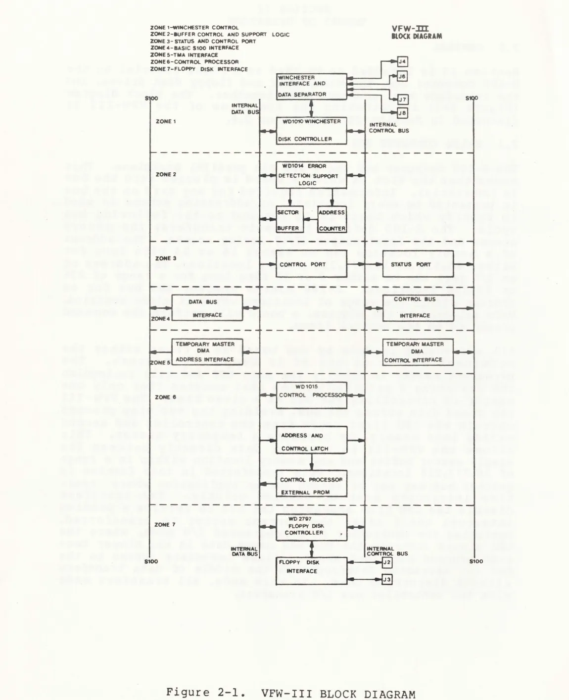
(10) SECTION II THEORY OF OPERATION --. 2. 0. GENERAL .. Section II is intended to be used as a light tutorial on the S-100 computer bus, the Winchester and floppy disk drives, and the interface that connects them together. The block diagram (Figure 2-1) illustrating the functions of the VFW-III is discussed in Section II, Subsection 2.4. 2.1. S-100 COMPUTER BUS. The S-100 computer bus has a 100 pin parallel backplane. This means that the slot in which a board is plugged into the bus is inrnaterial. Information required for any card on the bus is pr·esented to every location. An addressing scheme is used to specify which board is to respond to the following bus cycle. The S-100 defines two basic transfers; the memory access and the input/output (I/O) device access. The address of a memory location can be either 16 or 24 bits long for either 65,536 or 16,777,216 memory locations. The address of an I/O port can be either 8 or 16 bits long for a range of 256 or 65,536 locations. S-100 boards monitor the bus· for an address within the range of locations which it alone contains. Once selected by the address, a board w.ill perform the command presented on the control lines. All addressing is done by one board at a time; either the permanent master or one of 16 temporary masters. The permanent master is usually the main CPU and will relinquish the bus using a priority scheme that ensures that only one master is controlling the bus at a given time. The VFW-III can speed data across the bus, avoiding the two step process wherein the CPU first ·reads fr om the controller and second writes into memory, by becoming a temporary master. This allows the VFW-III to transfer data directly between its single sector buffer and any memory location within in a range of 16,777,216 locations. Data transferred in this fashion is quicker but may not be chosen for an application where realtime interrupts must be handled quickly. TMA transfers disable the CPU from accessing the bus to service a pending interrupt until after the current sector is transferred. Operating the controller in a programmed I/O mode, where the CPU always controls the bus and moves data in the slower twostep process described above, allows immediate access to the bus for servicing interrupts in the middle of data transfers without disturbing them. In this mode, all transfers made with the controller are I/O transfers.. 2-1.
(11) ZONE 1-WINCHESTER CONTROL ZOHE 2-8UFFER CONTROL ANO SUPPORT ZONE 3- STATUS ANO CONTROL POAT ZONE,-BASIC $100 INTERFACE ZONE S-TMA INTERFACE. VFW-III. LOGIC. llOCk DIAGRAM. --. ZOHE6-CONTAOL PROCESSOA ZONE 7-FLOPPY DISK INTERFACE. S'IOO. -. DATA SEPARATOR. -. INnANAL DATA BUS. J4. Je. -. WINCHESTER INTERFACE ANO. ). -. 51110. J7. I. .. I. WD1010 WINCHESTER. ZONE 1. -. J8. INTERNAL CONTROL BUS. -. DISK CONTROLLER. ........ - - -. -. -. -- --- -. - - - - _.... -. W010~ -. -. ZONE2. -. -. ~. ~. - -. -- - -. ._.. -. -. -. _._. - -. ._. -. _.. -- --. -. t. SECTOR. ADDRESS. -. BUFFER. ....... -. OETECTtON ·suPPORT LOGIC. -. .--.. ERROR. • -. ..... - -. ._. .-... ,._.,_ _.. COt.NTER. --. -.. .._., ._. - - --. - ..... - . -. ..._,. ---. ...-. ZONE 3 CONTROL PORT. --------~-. DATA. - -- - .... ~. -. STATUS PORT. -- ----. -. -~. -. ._. . -. CONT9'0l. aus. .. -. -. .... -- - - - - - -- ~. -. -~. - - ---. ~ _.. - - -. - -. ... ~. TEMPORARY MA.STEA. •us. ...... ~ . - - . ._.. -. TEMPORAR'f' MASTER. - -. OMA. ~. - --. INTERFACE. ~. ~ONE 5. -. ~. -. ZONE4..._______________ INTERFACE. -. ---. ....... -. - -. OMA COHTAOl INTERFACE. A.ODRESS INTERFACE. -- - - - -- -- - -- -. .... ._. - ...... ._.. - - - -. -. --~. - - -. -- - -. -. __.. -. .,...._.. --. W01015 -. CONTROL. .. ZONE 8. PA()CS:f;"""~-:;c-,....... _~. ADDRESS ANO. -. LATCH. CONTROL. •. CONTROl PROCESSOR. -. EXTERNAL PROM ii---. .-.. -. -. ---. ~. -. -. -. -. ---. -. -. ZONE 7. -. -. ._._.. ~. 5100. ...._... W02797 FLOPPY OtSI'. CONTROLLER. -. -. -. A..OPf>Y. -. ~. :. J2. 01$1(. INTERFACE. -. ...... -. -. ..... -. INTERNAL COHTROl BUS. 1. BUS. -~. .•. I I. INTERHAL ~TA. ...... $100. ... -------~J 3. ) Figure 2-1.. VFW-III BLOCK DIAGRAM 2-2.
(12) An interrupt bus is defined under the S-100 to stop the CPU to quickly do a time-dependent routine transparent to the present task. In~errupts are commonly used to get the CPU to transfer data with an input/output device and are more efficient than polling status loops where many wasted reads are made until the status changes, signalling an operation needed to take place. Status loops seldom respond as quick as interrupts. Data lines exist for moving either 8 bit bytes or 16 bit words during memory or I/O transfers. All data transfers to or from the VFW-III will be 8 bit byte length only • . 2.2. WINCHESTER DISK DRIVES. Winchester disk drives are rotating memory, random access storage devices which fulfill the need for fast, large, online data storage and retrieval. The word Winchester a c ·t u a 11 y r e f e r s t o th e t e c h n o 1 o g y . of .t he n i c k e 1- z i n c formulated read·/ write head, but is commonly used to refer to 5.25" hard disk drives. The term "Winchester disk drive" is used interchangeably with •hard disk drive" throughout this manual. A hard disk drive is a device which allows access to data stored magnetically within a vertical stack of several magnetic coated disks or platters. The stack is continuously spinning at speeds roughly 12 times as fast as a floppy disk drive with the read/write heads aerodynamically "flying" microns above each sur·f ace in the stack (two heads pe r platter; top and bottom). All heads are attached to an assembly som~times called an actuator ara, which can be controlled to position the heads in or out along ·t he radii of the stack. At any given position of the read/write heads, the magn~tic media spinning below it that could be read or written would trace out a circle on the media. This circle is called a track. At each position of the actuator arm, its associated track is assigned a trac·k number. Track numbe·rs range from zero at the outermost concentric circle to the maximum number located nearest the stack axis. The movement of . the actuator arm from one track to another is termed a seek and is issued by the controller as a series of pulses called steps. The time required to electically switch from one read/write head to ·another· above o·r below it is considerably less than the time taken to seek from one track to its neighboring ~rack. For this reason, when the end of one track has been reached, the continuation of information will be found on the same track number but on the next higher head number. The vertical stack of tracks accessed by all the heads of the actuator arm is referred to as a cylinder. Information in the present cylinder can be accessed the quickest. When consecutive data passes the end of a cylinder boundary, a seek must be issued and the head number is reset to zero.. 2-3.
(13) The OEM manual or product specification of every drive gives the unformatted capacity of the entire drive and of an. individual track. This is the number of locations where bits of information may reside. Since each of these bits cannot be uniquely addressed, a method is used that sacrifices some of the bits to identify blocks of continuous data. While this scheme is common among controller manufacturers, the identification blocks must be identical to allow information written by one company's controller to be read by another's. Th e VF w- I I I use s a wester n Di g it a 1 4 0 pin ch i p to hand 1 e th e foraatting or writing of the pattern required for subsequent reads and writes. As this chip gains popularity in the market place, com pa tibili ty among control le rs wil 1 increase. It is important to point out that more is involved than the physical access · to the old data. The driving software · must also be compatible. Each track is subdivided into units called sectors. The data field which contains the information to be read or written is accompanied by an identification or ID field and gaps before, between and following these fields. The ID field contains the "address" of the sector and includes the cylinder number, the head number and the sector number. This is the information that the Central Processing Unit (CPU) or host processor must provide to the controller board in order to transfer the associated data field. The controller takes all action nessessary to locate the target sector and transfer the data field between the drive and the controller's on-board single sect or buff er. All tr an sf e rs be tween the ho st and . the controller are independent of transfers between the controller and the drives. This means that the host needn't be "lockedup" as it waits to move data directly with the drive as· some controllers require. If programmed I/O ·mode is used to move data with the controller, any higher level interrupts or conditions requiring immediate action may be handled in . the middle of the transfer, only to complete it after the interrupt has been serviced.. An index pulse is used to the controller when a reference radius of the disk stack passes below the read/write heads. This reference is used to initiate formatting physical sectors, which are the actual · sector fields placed consecutively along the track. To increase the throughput or average rate at which information is transferred on a track, a technique known as sector interleaving is used. If physical sectors' ID fields contain consecutive numbers (an interleave factor of 1), a dilemma occurs when two sectors are to be read. As the first sector spins under the . read/write head, its ID field matches the target sector, and the following data field is transferred into the controller's single sector buffer. When the last bytes of data are read in, the cont ·r oller begins to move the saved data into the host system's memory, at the same time that the next target sector is spinning past the read/write head. The disk controller. 2-4. ).
(14) ). then returns, looking for the next target sector's ID field, and now must wait a full revolution for it to spin under • again. Sector interleaving makes a distinction between the physical sector and the logical sector. A logical sector is the next sector that the system would request, but its position is staggered around the disk so that while the buffer is moved into the host, unwanted sectors spin below the read/write head. Shortly after the controller returns, searching for the next logical sector, it spins under the head. The minimum interleave factor the VFW-III handles on a Winchester is 3; every third physical sector is the next logical sector. The table below illustrates an imaginary case where 16 sectors of 512 bytes length are formatted with an interleave factor of 3. Physical Sector Logical Sector 1st Revolution 2nd Revolution 3rd Revolution. 1 2 1 12 1 • • •. •. 12. 3 7 •. 7 •. 4 5 2 13 2 • • •. •. 13. 6 8 • 8 •. 7. 8. 3 14 3 • • • • 14. 9 10 11 12 13 14 15 16 9 4 15 10 5 16 11 6 • 4 • • 5 • • 6 9 • 10 • • 11 • • •. •. 15. •. •. 16. •. •. This shows that the entire track can be read in 3 revolutions with an interleave factor of 3 as opposed to 16 revolutions (1 per sector) for an interleave factor of 1 or 2. This increases the throughput by 5.3 times. The interleave factor is set only when a drive is formatted and is software selectable as explained in Section IV. An important misconception about the interleave factor is that it should always be set to the minimum value handled successfully by a disk controller. The proper interleave factor is dependent not only upon the time it takes the controller to empty its sector buffer, but also upon the average time between consecutive sector requests. This time may be lengthened by interrupt servicing or other computations between sectors, as may occur when searching files. If it is set too low, the next sector will spin under before the controller begins searching again, resulting in 1 sector per revolution. This throughput is much more noticeable on flopy disk drives where the magnetic media is spinning 12 times slower. The proper procedure for determining the interleave factor is to run benchmarks or timing tests in the final system using typical application software. 2.3. FLOPPY DISK DRIVES. A floppy disk drive can be considered to be a simpler version. ). of the hard disk drive discussed in Section II, Subsection 2.2. Only one removable magnetic disk is used in a floppy drive. A flexible plastic jacket protects and supports the media and has an open slot on front and back for the one or two read/write heads. Track densities are roughly 1/3 to 1/10 that of hard disk drives and rotational speeds are 1/12. Data. 2-5.
(15) ... is stored on the media using the same method described for Winchesters (ID fields, data fields, gaps and interleave factors).. ). Floppy drives vary, but their characteristics are usually some combinations of the following: 5.25~. or 8" sized diskettes and drives. Single or double density recording (FM or MFM). Single or double sided drives (1 or 2 heads). 48 or 96 tracks per inch track density. The VFW-III can handle a total of four floppy drives in any combination of the above characteristics with the appropriate driving software. · Removability is perhaps the greatest advantage of floppy disks. Large amounts of data may be backed-up or saved as redundant copies. The portability of · the diskette makes it a convenient way of transferring information between computers. Eight inch single sided, single density format is one of the few controller independent, standard formats. Using this format, files may be transferred to diverse computer systems. 2.4. VFW-III DISK CONTROLLER. The VFW-III is a single board, six layer disk controller capable of interfacing three hard disk drives and four floppy disk drives with minimal software differences. It is designed around the Western Digital 4 chip set: the WD1010, WD1014, WD1015 and WD2797. On-board processors and sector buffer make the board more bus efficient, handling all disk ·actions necessary to locate the target sector specified by the CPU. Error detection and correction are done by the controller's processors and require no work or supervision of the host.. The block diagram for the VFW-III shows connection to three busses: the S-100, the internal data bus and an internal control bus. Note that the S-100 bus is drawn on both sides for · clarity. Function has been divided into seven zones vertically and each is discussed in the following subsections. 2.4.1. Zone 1:. Winchester Control. The heart of the Winchester control circuit is the WD1010 Winchester Disk Controller. This circuit is located on the schematic on Sheets 4 and 5 and provides the hard disk drive positioning logic, write precornpensation logic and the data separator. The three drives are daisy-chained to the control connector J4 for selection. positioning and status signals-' Connectors JS, J6 and J7 link drives 1, 2 and 3, respectively, to transfer high frequency read and write data along differential 1 ines. J·umper 3, used in conj unction with bit 2. 2-6. ).
(16) of the control port (BASE+ OB), can be used to extend the h~ad addressing to 4 bits or 16 heads. New drives utilizing smaller Whitney read/write heads and internal spindle motors are making more than lOOMbytes of data available in a single standard size 5.25" drive. 2.4.2. Zone 2:. Buffer Control And Support Logic. -- . . .... This circuit is located on the top half of Sheet 2 of the schematic. The WD1014 Error Detection/Support Logic calculates the four bytes of appended ECC syndrome as data to be moved to or from the sector buffer which it controls. Assorted other signals are decoded within the WD1014 save space on the board. The address counter to the sector buffer is automatically incremented after every access and cleared when a command is issued to the command port at location BASE + 07H~ .. 2.4.3. Zone 3:. ... ... .... . -. .,,. ,. ~. .._. ... Status And Control Port. Located at the top left of Sheet 1 and the top center of Sheet 3 of the schematic, this circuit is used by the host to determine what the status of the board is and to define parameters for the next disk access. Section IV, Subsections 4.1.9 and 4.1.14 define their use in detail. 2.4.4. Zone 4:. Basic S-100 Interface. Sheet 1 and the left side of Sheet 3 of the schematic contain this circuitry. Address decoding, data bus buffering, interrupts, resets, wait states and power are the functions handled by this interface. Twelve ports are mapped onto this controller, and it decodes standard input/output device addressing as specified by the IEEE-696. All data transfers are eight bits wide, one software definable vectored interrupt may be selected and on-board reset may follow either pin 75 or 99. Jumper 20, when installed, will assert two wait states for every port access to the board. This is used for operation on a 6 MHz bus. 2.4.5. Zone 5:. TMA Interface. Most of Sheet 1 of the schematic is used to control temporary master access on the S-100 bus. The loadable address counters are used to select host memory for data transfers. The two buffers are used to control or hold the status and control signals of the bus during TMA, and the two programmable logic arrays are used to handle TMA priority resolution, and then to control both the internal and external busses. 2.4.6. Zone 6:. Control Processor. The control processor circuit on the lower half of Sheet 2 is designed around the WD1015. This device intercepts commands from the bus and converts them to what would · be required by 2-7.
(17) either the Winchester or floppy contoller chips. The external PROM enhances the internal program, offering more formats to be supported. The address latch is used both to address the PROM and to address the other 40 pin chips. Data is moved on the internal data bus by the control processor between the sector buffer and the Winchester· and the floppy controllers. When ECC errors less than or equal to five bi~s are detected, the WD1015 will perform the correction within the sector buffer before passing it on to the host. 2.4.7. Zone 7:. ). Floppy Disk Interface. The floppy disk interface on Sheet 3 allows control of both 8" and 5.25" drives of either density or head count. Drives are connected to J2 and J3 for 5.25" and 8", respectively. Since both cables are electrically common, unique unit numbers must exist on both cables and only one terminator may be connected •. •. ). 2-8.
(18) ... SECTION III SOF'IWARE DRIVERS 3.0. GENERAL. This section is intended to supply all necessary information to write or modify a software driver for the SDSystems VFW-III. Provided herein are the complete memory map of the controller and the command set for the commands. 3.1. MEMORY. MAP. The VFW-III is mapped onto the S-100/IEEE-696 using Standard Input/Output Device Addressing. Address lines A7 through A4 are compared with the I/O base address set by SWl positions 5 through 8 to determine if the board is to be selected. If so, address lines A3 through AO are needed to select locations within the memory map of the controller. These 16 locations are illustrated in the following table as offsets from the base address. --------------------------------~------------------------------. I/O Address. -----------------~-----. BASE+OO BASE+Ol BASE+02 BASE+03 BASE+04 BASE+OS BASE+06. Write Access. Read Access. ... ----------------------------------------. BASE+07 BASE+O 8. Sector buff er Error register Sector count Sector number Cylinder low Cylinder high Size/device/ head register Status register Not selected. BASE+09. Not selected. BASE+OA. Not selected. BASE+OB BASE+OC BASE+OD BASE+OE BASE+OF. Not Not Not Not Not. selected selected selected selected selected. Sector buffer Write precompensation cylinder Sector count Sector number Cylinder low Cylinder high Size/device/head register. Command register DMA address least significant byte DMA address most significant byte DMA address extended significant byte VFW-III control port Not selected Not selected Not selected Not selected. _ _ _ _ . . . _ _ _ _ _ _ _ _ _ _ _ _ _ _ _ _ _ _ _ _ _ _ _ _ _ _ _ _ _ _ _ _ _ _ _ _ _ _ _ i - . _ _ _ _ _ _ _ _ _ _ _ _ _ _ _ _ _ _ __. ). Note that when connecting W20 to enable two wait states for 6 MHz operation, the controller will also assert the wait for address BASE+OC through BASE+OF, even though these locations are not used. Other I/O cards requiring wait states for 6 MHz but not incorporating them within their designs may be mapped here.. 3-1.
(19) 3.1.l. Sector Buffer (Read/Write And Increment). A lK byte wide sector buffer, capable of containing only one sector regardless of sector size, is mapped into location BASE+OO. Except for READLONG and WRITELONG commands, all access to this location must be by block transfers equal in length to the sector size, using the quicker DMA mode or programmed I/O mode. On-board counters, which are reset at the issuance of a command. address the Random Access Memory (RAM), consecutively incrementing the address after each access. In programmed I/O mode, this port is simply continuously read or written by the host processor until a full sector length is transferred. In DMA mode, the transfer of data between the host's memory and the sector buffer is handled by making the VFW-III a temporary master. Provided that the absolute address has been loaded into registers BAS E+O 8, +O 9 and +OA and that the control port, BAS E+O B, has enabled DMA mode and selected the proper direction, then the controller will move the data around without need of the processor. 3.1.2. Error Register (Read Only) .. In addition to normal error reporting, this register will also hold the results of on-board diagnostics initiated by a powerup or by a test command. The diagnostic sequence starts with the WD1015 and progresses to the WD2797 or until the first error occurs wherein the error code is posted and the test terminated. Error codes for the internal diagnostics and their meaning are tabulated below. Note that the error bit of the status register will never indicate an error at the completion of the diagnostics.. ). -------------------------------------------------------------Error Meaning. Code. -------------------------------------------------------------0 All diagnostics ran error-free; test passed 1. 2 3 4 5. Error Error Error Error Error. found found found found found. within within within within within. the the the the the. WD2797 WD1010 sector WD1014 WDlOlS. Floppy Disk Controller Winchester Disk Controller buffer or internal bus Control Processor. -------------------------------------------------------------The error register is also used to determine the type of error encountered during the last command and is only val id if the status register (Section III, Subsection 3.1.9) indicates an error exists. An active high bit specif icies the errors illustrated in the following table.. ). 3-2. l.
(20) ...------------------------. -------------------------Error Bit. Error. Bit. ------------------------0 No data address mark 2 4. 6. -----------------~-------. 1 3. Command aborted ID field not found Incorrectable error. 5. 7. ------- ..... -------------------------3.1.2.1. Track 0 not found Not used Not used Bad block detect. ----~-------------. No Data Address Mark. A no data address mark error occurs if, after successfully finding the target sector's ID field or header, the subsequent byte marking the beginning of the sector's data field is not found with 16 bytes. Possible caused of this error include: bad diskette, media flaw after the ID field, or controller out of calibration. 3.1.2.2. Track 0 Not Found. Both floppy and Winchester drives assert a signal when their read/write heads are on track O. During a restore command, this signal is used to put the read/write heads in a known position by continuously stepping to a lesser track number and then testing the track 0 signal. If the drive does not assert the signal before 1024 steps are attempted, the VFW-III will post this error. One probable reason for receiving the error in conjunction with Winchester operation is that jumper W21 is not connecting C-2, meaning the common line jumpered to option 2 as shipped from the factory. The jumper corrects a design flaw in the LSI chip WDlOl0-00 Control Processor that made it incompatible with drives that did not deactivate the signal SEEK COMPLETE on the rising edge of step. Other possible reasons for this error are a bad cable .connection or a drive that has not had its read/write heads unlocked after shipping. Note that few 5.25" Winchester drives use head-locking for transport. 3.1.2.3. Command Aborted. Certain conditions must be reported by the disk drive before the operation of a valid command can commence. Failure of these conditions results in the po~ting of this error by the VFW-III. Interrogation of the status register will show one of the following signals in an abnormal state. 3.1.2.3.1. ). Status Register Bit 6:. Ready. The normal state for this signal is active high, which indicates that the drive is ready to read, write or seek. When a drive is disconnected, powered down or spinning up, this signal is inactive and forces an error if a command is sent to it.. 3-3.
(21) 3.1.2.3.2. Status Register Bit 5:. Write Fault. ). The normal state for this signal is inactive low. Write fault on a Winchester indicates that a condition exists at the drive that could cause improper writing on the disk such as bad DC ~voltages, improper head selection or write gate/write data problems. Floppy drives will assert this signal if a diskette is write protected. 3.1.2.3.3. Status Register Bit 4:. Seek Complete. Seek complete must be active high prior to execution of all commands except seek. It is used to signal that the Winchester read/write heads are stationary over a legitimate track, and it goes inactive low as the heads are seeking to another track. After a power-on, if the read/write heads are not over track O, a recalibration will be initiated by the drive, during which seek complete will go inactive. Floppy disk access forces this status bit active high since there is no seek complete signal on its interface. 3.1.2.4. Identification Field Not Found. If the target sector cannot be found by the drive after the retry sequence, this error is posted. A drive that has been formatted with too many sectors per track will cause this error as those sectors that were overwritten are sought. Media errors in the identification field and a VFW-III out of calibration also cause this error. 3.1.2.5. Uncorrectable Error. This error indicates that bad data was received from the disk drive. An uncorrectable error is set when CRC formatted sectors are read and the two bytes of appended CRC do not match the value calculated on the data. ECC formatted Winchesters will post this error if an error of more than five consecutive bits is received. The VFW-III automatically corrects single burst errors of five or less bits before transferring the data to the host. 3.1.2.6. Bad Block Detect. A bad block indicator in the identification field will force this error. Known media flaws that fall within the data field can be mapped out during the track format by inserting a bad block indicator within the identification field. Subsequent reads or writes to the sector will cause this error, allowing the host to take further action. 3.1.3. Write Precompensation Cylinder (Write Only). Since Winchester drives differ greatly in their number of cylinders, this register is provided to specify on which cylinder the Winchester controller activates both the REDUCE 3-4. ).
(22) WRITE CURRENT signal and the write precompensation logic.. Twelve nanoseconds is the fixed write precompensation delay from nominal. Floppy disk drive write precornpensation is not handled in this register and is unaffected by it. In order to address a range of 1024 cylinders by use of an eight bit register, the following method is used. The target cylinder must be divided by 4, shifting the bits to the right two places. For example, to load the register for a cylinder of 512 decimal, simply divide by 4 to get 128 decimal or 80 hexadecimal. Note that the two least significant bits of the resulting cylinder will be assumed to be zeroes. · 1 0 0 0 0 0 0 0 0 0 binary --->·l 0 0 0 0 0 0 0 binar·y. -. 200 hexadecimal. 1 0 0 0 0 0 0 0 1 1 binary --->l 0 0 0 0 0 0 0 binary. -. 203. 80 hexadecimal. --. -. 512 decimal. 128 decimal. hexadecimal -- 515 decimal 80 hexadecimal - 128 decimal. 3.1.4 ' Sector Count (Read/Write). The sector count register is used during multiple sector reads or writes to specify the number of sectors requested. A decrement of this register occurs after. every sector transfer. Format commands use this register to specify the number of sectors to format on the present track. 3.1.5. Sector Number (Read/Write). The starting sector number for multiple sector transfers or the target sector for single sector transfers is written into this register. When an error is encountered. this register can be read to identify which sector of a multiple sector transfer the error occurred on. 3.1.6. Cylinder Low (Read/Write). Seek, Read and Write commands cause this register and the next one to specify the cylinder at which the read/write heads are to be positioned. This register holds the eight least significant bits of a 10 bit cylinder number field • •. 3.1.7. Cylinder High (Read/Write). Seek, Read and Write commands cause this register and the previous one to specify the cylinder at which the read/write _heads are to be positioned. This register holds the two most significant bits of a 10 bit cylinder number field as illustrated below. Bit 8 of the cylinder field has an additional function when used with floppy disk drives. Disks formatted at 48 tracks per inch (TPI) can be read from a 96 TPI drive if bit 8 is set to 1. ). 3-5.
(23) Cylinder High. Cylinder Low. 7 6 5 4 3 2 1 0 x x x x x x 9 8 x x x x x x x *. 7 6 5 4 3 2 1 0. 3.1.8. ). Cylinder Registers Cylinder Number Field Floppy 48 or 96 TPI bit. 7 6 5 4 3 2 1 0. x x x x x x x x. Size/Device/Head Register (Read/Write). The Size/Device/Head register is used to select ECC or CRC operation, sector size, Winchester or floppy drive and head nu rn be r • The f o 11 ow in g tab 1 e i 11 us tr ates the use of the bi t s of this register. 7 0 1 x x x x x x. 6. 5. 4. 3. x x. x. x. x 0 1 0 1 x x x x x. 0 0. 1 1 x x. x. x. x. x. x. x x. x x x x x. x x. x x. x. x. x. x x. x. x. x x x x x x x x. x x. x. 3.1.9. x. x x x x. x x. x. x. x x x. x x x x x. 1. 0. x. 2 x. x. x. x. x. x. x. x. x. x. x. x. x x. x x x x. x x 0 0 1. x x 0 1 0. x x x. x. x. x. x x. x. x. * * * * * * * *1. * * * *. x 0 0 0 0. x 0. x. 1 1 1. 1. x x 0 1 0 1 0 1 0. *1. 1. 1. 1. x. x. 1. 1. 0. 1 1 1. 1 1 1. 1 1. 1 1. l 1. 1 1. 0 0 0 0 1 1 1 1. x 0 1 0. * *. *. 0 1 1 0 0. 0 1 1. 1. 0 0 1 1. 0 1 0 1. Size/device/head register bits Select CRC operation Select ECC Winchester operation Sector size = 256 bytes Sector size = 512 bytes Sector size = 1024 bytes Sector size = 128 bytes Winchester drive 1 select * Winchester drive 2 select * Winchester drive 3 select * Winchester head O Winchester head 1 Winchester head 2 Winchester head 3 Winchester head 4 Winchester head 5 Winchester head 6 Winchester head 7 Floppy disk drive select Floppy drive 1 head 0 Floppy drive 1 head 1 Floppy drive 2 head 0 Floppy drive 2 head 1 Floppy drive 3 head 0 Floppy drive 3 head 1 Floppy drive 4 head 0 Floppy drive 4 head 1. Status Register (Read Only). .•. The status register is used to present command completion information to the host processor and is only valid when BUSY (bit 7) is inactive low. Interrupts issued from the VFW-III are cleared when this register is read. The following table illustrates the bits in the register. 0 2 4. 6. Error encountered ECC correction made Seek complete Drive ready. 1. 3 5 7. 3-6. Not used Data transfer requested Write fault VFW-III busy. ).
(24) 3.1.9.l ). Error Encountered (Bit 0). An active high bit indicates that an error condition exists and that the host processor should next check the error register for further information. This bit is reset when the next command is issued. 3.1.9.2. ECC Correction Made (Bit 2). This bit indicates with an active high that a correction has been successfully made on the single sector transfer or that one or more corrections have been made during a multiple sector transfer. 3.1.9.3. Data Transfer Requested (Bit 3). The data transfer request goes active high when the VFW-III requires a sector's worth of data to be transferred between the host and the on-board sector buffer during a Read, Write or Format command. 3.1.9.4. Seek Complete (Bit 4). Winchester drives force the signal active high when the selected drive's read/write heads are correctly positioned over a track and deactivate it during power-up and during head movement. · When floppy drives are selected, this bit is activated when the size/device/head register is reloaded. 3.1.9.5. Write Fault (Bit 5). An active high of this bit indicates either that the selected Winchester drive is reporting a write fault condition or that the selected floppy disk drive to be written to is write protected. The command issuing the fault condition will be aborted. 3.1.9.6. Drive Ready (Bit 6). This bit indicates when active high that the selected Winchester drive is reporting that it is ready to execute a command. Floppy disk drives do not report this status through the interface; so it will be forced active whenever floppies are selected. 3.1.9.7. VFW-III Busy (Bit 7). Bit 7 must be inactive low for any bit within this register to be valid. An active level indicates that the VFW-III processor is busy and the internal data busy is inaccessible.. 3-7.
(25) 3.1.10. Command Register (Write Only). ). The command register when written to, initiates the command sequence. All other register describing the command must be enterred before the command is issued. Writing to this location will also clear the interrupt. 3.1.11. TMA Least Significant Byte (Write Only). This register is used to load the least significant byte (A7AO) of the memory location where the VFW-III Temporary Master Access is to start. This register must be reloaded prior to any TMA. 3.1.12. TMA. Most Significant Byte (Write Only). This register is used to load the most significant byte (Al5A8) of the memory location where the VFW-III Temporary Master Access is to start. This register must be reloaded prior to any TMA. 3.1.13. TMA. Extended Significant Byte (Write Only). This register is used to load the extended significant byte (A23-A16) of the memory location where the VFW-III Temporary Master Access is to start. This register must be reloaded prior to any TMA. 3.1.14. VFW-III Control Port (Write Only). The control port is used to supply additional information about the drive selection and the data transfer to take place. Use of these bits is illustrated below.. -----------------------------------------------------------Meaning Bit Meaning Bit ______________________ ... ______ _ ------------------------------0 8" full size floppy select 1 Extended head selection 2 4. 6. Single density select Temporary master access direction External PROM disable. 3 5 •. 7. --------------------------~-----. 3.1.14.1. Motor-on mode Temporary master access enable Not used. -------------------------~---. 8" Full Size Floppy Select {Bit 0). An active h i g h on th is s i g n a 1 i s used to s e 1 e ct 8" f u 11 ·s i z e d floppy disk drives, and an inactive low selects 5.25" minis. When Winchesters are to be selected, the register bit may be either value. 1 0 X. = 8" floppy drives = 5.25" floppy drives = 5.25" Winchester operation 3-8. ).
(26) 3.1.14.2. Extended Head Selection (Bit 1). If jumper W3 is changed from its factory setting such that pin 2 is connected to common, this signal will be driven onto the Winchester interface in place of the signal REDUCE WRITE CURRENT (J4 pin 2). This is the pin/ used by Winchester drives containing more than eight read/write heads to extend the head selection up to 16. The size/device/head register will still decode head select bits 2 to O. This register is used as head select bit 3. 1 = Head numbers 8 to 15 0 = Head numbers 0 to 7 3.1.14 •.3. Single Density Select (Bit 2). Bit 2 is used to choose single density or double density floppy disk access and has no effect on Winchester operation.. = Single density 0 = Double density X = Winchester operation 1. 3.1.14.4. Motor-On Mode (Bit 3). This bit is used to select timing for either the MOTOR ON signal for 5.25" floppies or the HEAD LOAD signal for 8" floppies when jumper Wl is in its factory setting (pin 1 connected to common). Floppy drives requiring a spi~ down when inactivated need this bit set active high. After 3 seconds without an access, the motor will be turned off. Drives requiring a BEAD LOAD signal, such as full sized floppies, should have this bit set inactive low. 1 = Motor-on timing 0 = Head load timing X = Winchester operation 3.1.14.S. Temporary Master Access Direction (Bit 4). S-100/IEEE-696 Temporary Master Accesses (DMA) use this bit to determine if the direction is from the host into the on-board sector buffer or if it is the reverse. 1 0. = From = From. the sector buffer to the host (read commands) the host to the sector buffer (write and format commands). 3.1.14.6. Temporary Master Access Enable (Bit 5). This bit enables the VFW-III when it needs data from the host f·or READ, WRITE and FORMAT commands to make a S-100/IEEE-696 Temporary Master Access for the data. The current values in the TMA address registers (BASE+08, +09 and +OA) are used as the starting locations for the host memory buffer. After an 3-9.
(27) •. ). access has occurred. the address registers will be pointing to the next location a f ter the last byte addressed in host me mory but may change while idle between commands. For this reason the address r egi s ters mu s t be reloaded to the beginning of a block before issuing a command using TMA. 1 = TMA enabled (DMA mode) 0 = TMA disabled (Programmed I/O mode) 3 .1.14.7. Ex t e nde d PROM Di sabl e (Bi t 7). An active h i gh bit in this registe r will disab le the e xternal PROM containing single density format routines. It i s advised that this bit be maintained as O, enabling the external PROM . 1 = Disable external PROM 0 = Enable external PROM 3.2. VFW-III COMMAND SET. The command set for the VFW-III can be broken down into Type 1, Type 2, and Type 3. Type 1 commands involve no data transfers and include Restore, Seek and Diagnostic Test. Type 2 commands involve data transfers from the selected drive to the host's memory and include all Read commands. Type 3 commands involve transfers from the host's memory to the selected drive. All Write commands and the Format command are of Type 3. The commands are illustrated in the table below. Rest or e Seek Test Read Write Format. Type Type Type Type Type Type. 1 1 1 2 3 3. s -- St epping rate: D - Read Interrupt: M -- Multiple Sectors: L - Long Mode:. 0 0 1 0 0 0. 0 1 0 0 0 1. 0 1 0 1 1 0. 1 1 1 0 1 1. s s s s s s s s 0 0 ML ML 0 0. 0 D 0 0. 0 0 0 0. Defined in Section 0-Programmed I/O 0-Single 0-Normal. lOh 70h 90h 20h 30h 50 h. - lFh - 7Fh - 2Eh - 36h. III, Subsection 3.2.1 1-DMA 1-Multiple 1-Long. •. 3.2. 1. Type 1 Commands. Type 1 commands involve no data transfers. but most require stepping rates to be specified. The stepping rates in the following table are used as bit 3 through 0 within the Restore or Seek command and are saved internally for subsequent implied seeks.. ) •. 3-10.
(28) Rate Number. B3-BO. Winchester. Floppy. ooa. OOOOb OOOlb OOlOb OOllb OlOOb OlOlb OllOb Olllb lOOOb lOOlb 1010b lOllb llOOb llOlb lllOb llllb. 0.035 ms o.s ms 1.0 ms 1.5 ms 2.0 ms 2.5 ms 3.0 ms 3.5 ms 4.0 ms 4.5 ms 5.0 ms 5.5 ms 6.0 ms 6.5 ms 7.0 ms 7.5 ms. 0.015 1.0 2.0 3.0 4.0 5.0 6.0 7.0 8.0 9.0. Old 02d 03d 04d. 05d 06d. 07d 08d 09d lOd lld 12d 13d 14d 15d 3.2.1.1. OOh Olh 02h 03h 04h 05h 06h 07h 08h 09h OAh OBh OCh ODh OEh OFh. 10.0. 11.0 12.0. 14 .o. 15.0 16.0. ms ms ms ms ms ms. ms ms ms ms. ms ms ms ms ms ms. Restore Command. A Restore command causes the selected drive to step the read/write head toward track 0 until the drive signal TRK 00 goes active. The stepping rates specified in bits 3 through 0 are saved for subsequent implied seeks and used as the step rate for th is com rnand unless a floppy step rate 1 ess than 8 ms is given. In that case the value chosen is stored, but the step rate for the restore is set to 8 ms. The cylinder high and cylinder low registers are cleared before stepping begins. After each step is issued, Ready and Write Fault are sampled for their normal levels. If no error conditions occur, the VFW-III will wait up to 16 revolutions for the Seek Complete to go active. The interface signal TRK 00 is next sampled to determine if the read/write heads have found track O. If not, then a step is produced and the procedure is repeated until either track 0 is found or 1024 steps have been attempted.. Jumper 21 on the VFW-III has been incorporated to correct an inherent problem with the WDlOl0-00. This LSI chip requires the Seek Complete signal to be deactivated immediately following the rising edge of the step pulse. Many 5.25" Winchester drives deactivate Seek Complete after the falling edge of the step pulse, resulting in the WDlOl0-00 seeing an apparent early Seek Complete to which it responds with the next step pulse. Therefore, during a restore command on these drives, the chip would issue two steps at a time. Some drives make a "chattering" noise while continually trying to seek past track O, after starting on an odd numbered track. With jumper 21 connecting pin 1 to common, this may occur if one of these drives is cabled in. If jumper 21 is connecting pin 2 to common. the Seek Complete from the drive is modified onboard to ensure that an early deactivation occurs. This jumper selection allows operation with either type of drive and is therefore the factory setting and recommended choice.. 3-11.
(29) 3.2.1.2. Seek Command. Due to the capability of implied seeks for Read and Write commands, the use of the Seek command is limited to positioning the read/write heads for formats, or issuing concurrent seeks to multiple drives using buffered seeks. Since a Seek command does not test the value of Seek Complete before or after the command, several seeks can be initiated and status checked to determine which drive finds its target cylinder first by monitoring bit 4 of the status register. Note that the stepping rate is both used and saved for subsequent implied seeks. 3.2.1 •.3. Diagnostic Test Command. The power-up self diagnostic test described in Section III, Subsection 3.1.2 can be reissued by use of the Diagnostic Test command. A test starts with the WD1015 and progresses to the WD2797 or until the first error is encountered wherein the error code is posted in the error register but an error is not signified in the status register as would normally be done. Error codes. for the internal diagnostics and their meanings are tabulated below. Error Code 0 l 2 3 4 5. 3.2.2. Meaning All diagnostics run and indicating no errors. Error found within the WD2797. Error found within the WD1010 Sector buffer error Internal bus or WD1014 error WD1015 error. Type 2 Commands. Commands moving data from the disk drives to the host's memory are of Type 2. These are the two read commands, Read and Readlong. Read commands will activate implied seeks at the 1 as t step rate to the tar get track if ne s ses sa ry. All other registers describing the transfer must be loaded prior to executing Type 2 commands. 3.2.2.1. Read Command. This is the common Read command used to retrieve data from sectors on Winchesters or floppies. CRC will be checked and eight retries will be made before errors are reported. If ECC is formatted on a hard disk drive, data errors will force verification of the syndrome bytes followed by autocorrection of errors less than six bits long. If two syndromes do not match in eight attempts, errors will be posted and the read terminated. Bit 3 (D) is set active high to disable the interrupt request with every byte. This is used in TMA operations where the interrupt will be asserted after the buffer has been transferred. When using multiple sector 3-12. ).
(30) transfers, this mode will always be used. If bit 3 is set inactive low, an interrupt will be asserted for every byte request made while moving data into the sector buffer. 3.2.2.2. Readlong Command. The Readlong command permits recovery of the data field and the four bytes of appended ECC syndrome on Winchesters formatted in ECC mode. This can be used in testing or for host correction beyond the WDlOlS's limit of five bits. 3.2.3. Type 3 Commands. Transfers from host's memory through the sector buffer to the disk drive are performed by the three Type 3 commands. · Implicit seeks will be executed as nessessary for the Write and the Writelong commands. 3.2.3.1. Write Command. Data is stored within the data field of the specified sector using this command. ECC or CRC are automatically appended to the data field as it is being written to the drive. It is recommended that, when using programmed I/O transfers, block moves be made without consulting the data request line of the status register between all bytes. ). 3.2.3.2. Writelong Command. This command, which can be used to test the ECC recovery, allows the writing of a host-supplied four bytes of syndrome and a data field. 3.2.3.3. Format Command. Before any new disk can be used, it must be formatted with a pattern of ID fields, data fields and gaps. No reads or writes will be completed on unformatted media. The Format command requests, from the host, a full sector of information containing the interleave table. It is important to understand that even if the interleave table is only 18 bytes long, as with nine sectors of 1024 bytes, a full sector must be transferred to the .buffer. After the information fills the sector buffer. the track will be formatted according to the specified format after the next index pulse is found. The interleave table has two entries per sector. The first byte is set to OOH for normal sectors and set to FFH if a sector is to be marked as bad. Sectors marked in this way will issue a bad block error . when read to allow the operating system to map the sector request to a reserved sector. The second byte contains the logical sector number and is a function of the desired interleave factor. An example of the first few bytes of the example mentioned above is illustrated with an interleave factor of 2. 3-13.
(31) ·oo. 02. 00. 04. 00 00. 09. 00. 07 05. xx. xx. xx. xx. xx. 00 00. 06. 00. 01 08. xx. xx. xx. FF. 03. xx xx. xx xx. Note that logical sector 3 (physical sector 5) has been marked as a bad block and that all other locations within the 1024. bytes transferred to the sector buffer are unimportant (marked here with "x" for don't-cares).. .•. 3-14.
(32) SECTION IV INSTALLATION. ). 4.0. GENERAL. Section IV is intended to assist in the installation of the VFW-I I I into ex is ti.ng systems. Al 1 inf or ma ti on involved in the physical integration of the controller is supplied herein. Requirements of the host system, settings and adjustments to the board, and cabling to the disk drives are explained in the following subsections. Note that the board comes calibrated from the factory for standard floppy disk drives and 5 MHz data rate Winchester disk drives; therefore, it is properly calibrated for most applications. The procedure below is included. for those exceptional cases requiring recalibration. 4.1. POWER AND COOLING. Section 3 of the IEEE publication, Std 696-1983, specifies the voltage levels of the +8 volt power pins of the S-100 that are to be considered compliant with its standard. Instantaneous minimum voltage must be greater than +7 volts, and instantaneous maximum voltage must not exceed +25 volts. Average maximum voltage must be less than +11 volts. This power is connected to the two voltage regulators of the VFW-III via S-100 pins 1 and 51. Two regulators are used to supply the typical 2.5 amps current required of the +5 volt level on-board, for heat dissipation reasons. At the average maximum voltage level of +11 volts, 15 watts must be dissipated. Two widely separated regulators with heatsinks below the IEEE-696 0.5" height limit allow operation up to +500C ambient air temperature. Adequate air circulation must be provided to prevent the heatsinks from raising poorly circulated air beyond this maximum temperature. 4.2. CABLES. All cable connectors for the VFW-III are positioned on the top edge of the board between the two voltage regulators. Pin 1 for J2 through JB is located in the lower left corner of each connector. J2:. 34 Pin. J3:. 50 34 12 20. J4: JS: J6: J7: JS:. 4.2.1. Pin Pin Pin Pin 20 Pin 20 Pin. •. 5.25" Floppy ·Disk Drive Connector 8" Floppy Disk Drive Connector 5.25·" Winchester Disk Drive Control Connector . Test Connector Device l; Winchester Disk Drive Data Connector Device 2; Winchester Disk Drive Data Connector Device 3; Winchester Disk Drive Data Connector. Floppy Disk Drives. The SDSysterns VFW-III controls four diverse drives concurrently through two connectors, J2 and J3, which are used to interface with 5.25" and 8" drives. respectively. 4-1.
(33) Leaving these connectors are 34 and 50 strand cables that attach the drives in a daisy-chain manner. Signals on J2 and J3 a re electrically common; so unique device numbers must reside on each cable.. ---J2: ... ---------.--------------5.25" Floppy Disk. ---------~-------------. _____ J3:. ---~---------.-.------------. Pi n. Signal. -------------------------6 DS4*. 26. INDEX* DSl* DS2* DS3* MOTOR-ON* DIR* STEP* WR DATA* WR GATE ~ TRK 00*. 28. WR PROT*. 30. RD DATA* SIDE*. 8. 10 12 14 16. 18 20 22 24. 32. 4.2.2. .... _________________ 8" Floppy Disk ___ Signal. Pin. ---- - --------- ------ -~~--. TG43* SIDE* HLD* INDEX* READY* DSl* DS2* DS3* DS4* DIR*. 6 14. 18 20 22 26 28 30 32 34 36. STEP*. WR DATA* WR ' GATE* TRK 00*. 38 40. 42 44. --------------------------. ). WR PROT*. __________ _____________ 46 RD DATA* _ _... Test Connector. Signals required for calibration and tro uble-shoot i ng a r e brought to connector JS for easy access.. -----------------------JS: Test Connector ------------------------Pi n Signal. - ~- - -- -- --- ---. JS :. -----------------------VCO IN 2. DRUN*. RDATA T3 9 Tl 11 GND______ _ _____________________. ... 4. WPCD*. 6. RC* T2 TEST*. 8 10. 12 GND __________ _________ .... __ _ ._. _.. 4.2.3. Test Connector. ----------------------Si gnal Pin. ---------------.----------1 VCO OUT 3 5 7. ... ---------. Winchester Disk Drives. The VFW-III is designed to interface up to three Winchester hard disk drives supporting the ST506/412 standard interface. Each drive requires the connection of two cables: the 34 pin control cable and the 20 pin data cable. All drives are attached via the control cable in a daisy-chain manner to J4, and each is connected through a unique data cable to J6, J7 or JB.. 4-2. ) }.
(34) ). ----------------------------------------------------------J4: Winchester Control J4: Winchester Control ----------------------------------------------------------Pin Signal Signal Pin ----------------------------------------------------------2 RWC* or HD3* 20 INDEX* HD2* WR GATE* SEEK COMPLETE* TRACK 00* WR FAULT* HDO* HDl*. 4. 6 8 10 12 14 18. 22 24 26 28 30 34. READY* STEP* DSl* DS2* DS3* DIR*. ------------------------------ ---------------------------------------------------------------------------------------J6, J7, J8: Winchester Data J6, J7, J8: Winchester Data ----------------------------------------------------------Pin Signal Pin Signal ----------------------------------------------------------11 GND 12 GND ). 14. 16 18 20. +MFM WR DATA GND +MFM RD DATA GND. 13 15 17 19. -MFM WR DATA GND -MFM RD DATA GND. ------------------------------ -----------------------------4.3. JUMPERS AND SWITCHES. SDSystems increases the flexibility of the VFW-III with the inclusion of user selectable jumpers and switches. The following subsections define both these electives and the factory settings. 4.3.1. Jumpers. Twenty-one jumpers reside on the VFW-III and are labelled with a "Wnn" specification, where "nn" is the associated number. The fol lowing 1 ist gives the 1 oca ti on, pin out, function and factory setting {preceded by an asterlsk) for all jumpers.. -------------------------------------------------------------JumperlPinoutlSettingl Location and Function ------1------1-------1----------------------------------------. Wl. I I I I I. 1. c 2. I I *C-1 I I C-2 I. I Located between Ul6 I Connects the floppy I the WD1015 to the I Connects the head I the WD2797 to the. and US. motor-on line f rorn floppy disks. load signal from floppy disks.. -------------------------------------------------------------4-3.
(35) ------ .... ----------~._. _____ ... ______________________________ _____ _ ._... __.. Jumper Pinout Setting I. Location and Function. -----------------1---------------------------------------W2 I Located between US and U9. 1 C 2. *C-1 C-2. I Enables write precornpensation on floppy I disks starting at cylinder 44. I Disables write precompensation on all I floppy disks.. -----------------l---------------------------------------W3 I Located between Ul2 and Ul3. *C-1. 1. C 2. C-2. -----_ ____ -------W4 ..... 1 C. 2. C-1 C-2. ------- ------ -.------ws I. 1 2. *1-2. .. 1 2. I Connects the reduce write current line to pin 2 of the Winchester interface. Connects the extended bit of the head select address to pin 2. ~----------------------------------------------. Located between U4 and UlS. Unused at this time. Unused at this time.. ---------------~------------------------------. Located between U21 and U22. Installs the 20 MHz oscillator (in etch). Isolates the 20 MHz oscillator.. -------- _____ ------- --.---------------------------------------------_.. W6. 1 2 ------. ------. *1-2 1 2. -------. W7. *1-2. 1 2. 1 2. ------ -----------.wa 1. 2 c. I. 3. I *C-1. C-2 C-3. ------------1-----W9 I I I. 1. 1-2. 2. *l 2. ------------1-----WlO I I I I. 1. c 2. ------1-----Wll I. C-1 *C-2. --------. Located between VR2 and U26. Installs VCO input signal (in etch). Isolates VCO input signal.. _ _ _ _ _ _ _ _ _ _ _ _ _ _ _ _ _ _ _ _.... _ _ _ _ _ _ _ _ _ _ _ _ _ _ c.- _ _ _ _ _ _ _ _. Located between U28 and U29. Enables WD1015 external addressing (in etch). Disables use of external PROM. ------------.,---------~----------------------. Located between Ul6 and 030. I External 2716 PROM (in etch). External 2732 PROM. Host bank selection.. --------------------~------------.------------. Located between U29 and U30. Disables internal PROM. Enables internal PROM.. • ----~-----~--------------------------.-.-----. Located between U44 and U45. POC* resets the board. RESET* resets the board {in etch). ________________ .... ___________ _____ __________________ _ ._... _... Located below U43. Command Complete interrupt asserts 1-2 I 1 vectored interrupt O, VIO*. I 2 1 2 Isolates VIO*. I - ---- -- - -- - - - ---------- --- - ------ - --- ---- .... - - - - .... - .... -- -- -- - ........ - .... - - - .... _. _,_.. _.. ~. ~ ~. _.._...,. -~. J. 4-4.
(36) ----------------~--------------------------------------------------. ). JumperlPinout Setting!. Location and Function. ______ ,______ -------1----------------------------------------. Wl2. I I I I. I Located below U43. I Command Complete interrupt asserts I vectored interrupt 1, VIl*. I Isolates VIl*.. 1-2. l 2. 1 2 ,_______________________________________ _ ------1------ _______. Wl3. I I I I. I Located below U43. I Command Complete interrupt asserts I vectored interrupt 2, VI2*. I Isolates VI2*.. 1-2. 1. 2 1 2. ------1------------)---------------------------------------Wl4 I Located below U43. I 1 2. I Command Complete interrupt I vectored interrupt 3, VI3*. I Isolates VI3*.. 1-2. 1 2. asserts. -----------1-------1---------------------------------------WlS I Located below U43.. ------. 1 2. I Command -Complete interrupt asserts I vectored interrupt 4, VI4*. 1 2 I ______ Isolates VI4*. ------... __________________________________ _._ 1-2. ------. Wl6 1 2. -------. Located below U43. Command Complete interrupt asserts vectored interrupt 5, VIS*. Isolates VIS*. _______________ ... ____________________ _. 1-2. 1 2 ------ ------__. Wl7 1 2. 1-2. ------- __..____. Wl8. 1 2. 1 2. ------1-2 1 2. ,_. Located below U43. Command Complete interrupt vectored interrupt 6, VI6*. Isolates VI6*.. asserts. ---------------------------------~------. Located below U43. Command Complete interrupt vectored interrupt 7, VI7*. Isolates VI7*.. asserts. --------------------------------------------------------Wl9 Located between U38 and U54. 1 2. *l-2 l 2. ----------------W20 ------. 1 2. 1-2. ---~--. *l 2 -------. W21. 2 C l _______________ ,..... *C-1. Installs VCO output signal (in etch). Isolates VCO output signal. -----~---------------.----------------------. Located between U31 and U32. Installs 2 wait states on every VFW-III I/0 access. No wait states used. _________________ ______________ _______ __ _... Located between Ull and Ul8. Deactivates the Winchester Seek Complete signal early. Normal Seek Complete timing. ..... _____________________ __________________ _. ________C-2_ _______ ~. _.. _.. _._. >; .. 4-5.
(37) 4.3.2. Switches. Input/Output (I/O) port addressing and the Temporary Master priority are selected via the eight position dip switch, SWl.. -I u I ( ( (. OFF ) 0. ). OPEN}. I I I I I I I I I I. Swl Sw2 Sw3 Sw4. I I I I I Sw5 I Sw6 I Sw7 I Sw8 I ___ I. ( ON (. 1. Swl: Sw2: Sw3: Sw4:. ) ). (CLOSE). Sw5: Sw6: Sw7: Sw8:. Temporary Master Priority Bit 3 (MSB) Bit 2 Bit 1 Bit 0 (LSB) I/O Port Decode Adr 7* (MSB) Adr 6* Adr 5* Adr 4* (LSB). Switch positions Swl through Sw4 are used to select the priority of the VFW-III Temporary Master bus arbitration. The highest prio~ity in the following table is OF, and 00 is the lowest.. ___________ ____________ _______________________ Pri Swl Sw2 Sw3 Sw4 _.. --------~----------------. Pri. Swl. Sw2. Sw3. Sw4. _.. ------------------------00 OFF OFF OFf OFF OFF OFF OFF OFF OFF OFF OFF. 01 02 03 04 05 06 07. OFF OFF OFF ON ON ON ON. OFF ON ON OFF OFF ON ON. 08 09 OA OB. ON OFF ON OFF ON OFF ON. ON ON ON ON ON ON ON ON. oc. OD OE OF. OFF OFF OFF OFF ON ON ON ON. OFF OFF ON ON OFF OFF ON ON. OFF ON OFF ON OFF ON OFF ON. ---------------------------. ---~-----------------------. Switch positions SwS through Sw8 are used to select the base address used in the IEEE-696 Standard Input/Output Device Addressing. Sixteen consecutive locations from the base address are decoded by the VFW-III. .•. -------------------------Sw6 Sw7 Sw8 I/O Sw5_________________ __________. __ ______________________ Sw5 ..... Sw6 Sw7 Sw8 I/O _ _________ ________________. ON ON ON ON ON OFF ON ON ON ON OFF ON ON OFF OFF ON ON OFF ON ON ON OFF ON OFF ON OFF OFF ON ON OFF OFF OFF ,_,...., .... _______________. ON ON ON OFF ON 90 ON ON OFF ON AO OFF OFF OFF ON BO co OFF OFF ON ON OFF DO OFF OFF ON EO OFF OFF OFF ON OFF OFF OFF OFF FO _____________ .... __________. _.. ..,.... 00. 10 20 30. 40 50. 60 70 ... _... ___. 80. 4-6. OFF OFF OFF. ) I.
(38) 4.4 ). CALIBRATION. The VFW-III comes calibrated from the factory for standard floppy disk drives and 5 MHz data rate Winchester disk drives; therefore, it is properly calibrated for most applications. The · procedure below is included for those exceptional cases requiring recalibration. Floppy adjustments can be made on a single trace oscilloscope, but Winchesters require a dual trace scope for proper results. All signals required for display are conveniently supplied on the 12 pin connector, JS. 4.4.1. Test Mode For The VFW-III. Prior to attempting any calibrations of Section IV, Subsection 4.4.2 or 4.4.3, the following procedure must be executed.. .. ). 1). Remove the jumper connecting JS pins 10 and 12 if installed.. 2). Assert a RESET pulse on the S-100 bus (pin 75 active low).. 3). Output a OlH to the VFW-III I/O port address, BASE+OBH. For factory setting of BASE equaling SOH, output the OlH to port SBH.. 4). Install the jumper connecting JS pins 10 and 12.. The board is now in test mode wherein some signals are redefined to aid in calibration. For this reason it is imperative that the jumper connecting JS pins 10 and 12 be removed before normal operation. 4.4.2. Floppy Disk Controller Calibration. Three points must be adjusted for proper operation of the WD2797 Floppy Disk Controller. These components are the trim capacitor C29 and the two trim potentiometers R7 and RB. Test connector pins used in this operation are: -----------------------~----------------------------------------. Pin. Signal. Function. • ------------------------------------------------~---------------. 7. 8 9. 10 11 12. Used to adjust the read pulse width to I/8th.of the read clock. T2 Used to adjust the write precompensation timing. Tl Used to adjust the center frequency of the internal voltage controlled oscillator. TEST* WD2797 input to enable test mode. GND Ground potential reference for the oscilloscope. TESTGND* A plug connecting pin 10 with this GND; enables test mode.. T3. -------------------------------------------------..----------------4-7. -~.
(39) 4.4.2.1. Floppy Disk Write Precornpensation. After entering test mode per Section IV, Subsection 4.4.1, connect T2 (JS pin 8) to a positive-edge triggered oscilloscope. Adjust the multiple revolution trim potentiometer, R7, until the active high pulse width of T2 equals the desired write precompensation value. Remove the jumper connecting JS pins 10 and 12 before normal VFW-III operation is attempted. 4.4.2.2. Floppy Disk Read Pulse Width. After entering ~est mode per Section IV, Subsection 4.4.1, connect T3 (JS pin 7) to a positive-edge triggered oscilloscope. Adjust the trim potentiometer, RB, until the active high pulse width of T3 equals 250 ns. Remove the jumper connecting JS pins 10 and 12 before normal VFW-III operation is attempted. 4.4.2.3. Floppy Voltage Controlled Oscillator Center Frequency. After entering test mode per Section IV, Subsection 4.4.1, connect Tl (JS pin 9) to a positive-edge triggered oscilloscope. Adjust the single revolution trim capacitor, C29, with a nonmetallic screwdriver until the period of the 50% duty cycle signal Tl equals 2 microseconds. Remove the jumper connecting ~5 pins 10 and 12 before normal VFW-III operation is attempted. 4.4.3. Winchester Voltage Controlled Oscillator. Trim capacitor C47 must be adjusted for proper operation of the Winchester data separator circuit. The following procedure defines how to calibrate the VCO using an oscilloscope, a nonmetallic screwdriver and a cabled-up Winchester drive. 1). Connect the Winchester control cable to J4 and the data cable to J6, J7, or JS as appropriate for device number 1, 2, or 3, respectively. Turn the Winchester power on and select the drive by writing to the SDH register at the VFW-III I/O BASE+06H (factory setting would be 56H).. ----------------------------------SDH Winchester. _____________________ .... ________________ ·orive Value_ Connector 1 2. J6 J7. 3. JB. 00 08 10. -----------------------._.------~--------. 2). •. Connect one lead of a positive-edge triggered oscilloscope to VCO OUT (JS pin 1) and either a second lead or a voltage meter to VCO IN (JS pin 2). 4-8. '.
(40) 3). Using the nonmetallic screwdriver, adjust the single revolution trim capacitor until a frequency of twice the drive's data rate "locks on." This can best be observed by displaying several clock periods; the oscilloscope will display clock periods farthest from the triggered edge as "fuzzy" until the phase-locked loop "locks on," resulting in a sharp image.. 4). After the frequency is locked on, tune C47 until the voltage on VCO IN is at 2.SV±O.SV.. 5). Connect RDATA and RC (JS pins 5 and 6) to the oscilloscope and fine tune C47 until the rising edge of RDATA is centered between any two voltage transitions of. ). RC.. The Winchester VCO is now calibrated. Remove the jumper between JS pins 10 and 12 if not previously done.. 4.5. NON-IEEE-696 BUSSES. S-100 busses not complying with the IEEE-696 standard may still control the VFW-III but may not take full advantage of its features. The most obvious change involves the specification of the Temporary Master Access (TMA) priority scheme. 4.5.l. Pin Assignments. The IEEE-696 standard specifies pins 20, 53 and 70 as new ground pins. Some older busses and modified systems may have these pins defined otherwise. If no better compromise exists, care should be taken to cut the connection between the pin and its feedthrough hole to the ground plane. The controller is a six layer board, and careless cutting could damage internal traces. The factory setting for the reset pin is laid in etch on the solder side of the board at jumper WlO. It is located between U44 and U45 and is set to reset the board when pin 75, RESET*, is active low. Removing this etch and connecting the common pad to pad 1 (see Section IV, Subsection 4.4.1) will force the board to be reset when POC* (power-oQ clear) is asserted low. Most S-100 boards support RESET*; so this change is seldom nessessary. Pin 25 has been redefined to be pSTVAL* instead of. The VFW-III only asserts this line when acting as a temporary master; this mode probably will not be used on non-IEEE-696 busses. Since this pin is not used as an input, operation in programmed I/O mode is unaffected. In this mode, the eight extra address lines of the TMA addressing circuit are not driven, thereby avoiding any conflicts on their pins.. 4-9. ~2..
(41) 4.5.2. Data Transfer Modes. ). The IEEE-6 96 defines. a Direct Memory Access (OMA) scheme and its priority resolution procedure which allow several devices to make DMA transfers without collision. This method is not backward compatible and therefore probably cannot be used on non-IEEE-696 busses. With programmed I/O transfers, whereby all data is transferred through the Central Processi~g Unit (CPU) between its memory and the disk controller, -no bus incompatibilities should exist. ~l transfers would be simple input/output commands to one of 12 ports.. 4-J.n.
(42) SECTION V SPECIFICATIONS 5 .O. GENERAL. Section V contains the specifications for proper operation of the VFW-III controller. 5.1. POWER REQUIREMENTS. Section 3 of the IEEE publication, Std 696-1983, specifies the voltage levels of the +8 volt power pins of the S-100 that are to be considered compliant with its standard. Instantaneous minimum voltage must be greater than +7 volts, and instantaneous maximum voltage must not exceed +25 volts. Average maximum voltage must be less than +11 volts. Zero voltage potential or Ground must be supplied on pins 20, SO, 53, 70 and 100. For non-IEEE-696 busses refer to Section IV, Subsection 4.5 for information concerning possible conflicts with the new ground pins. The VFW-III typically requires 2.5 amps at 5 volts. 5.2. ENVIRONMENT. Ambient air temperature may range from 0 to soo Celsius with a noncondensing, relative humidity between 20 and 80 percent. Adequate airflow must be maintained as discussed in Section IV, Subsection 4.1 to prevent the two voltage regulators f rorn excessively heating local air beyond this maximum value. Busses with the average maximum voltage of 11 volts on the +8 volt line will force the heatsinks to dissipate 15 watts; so proper airflow is important.. •. 5-1.
(43) ). THIS PAGE INTENTIONALLY LEFT BLANK. ). . 5-2.
Figure
Related documents
Upon receipt of the Read Sector command, the head is loaded, the Busy status bit set, and when an 10 field Is encountered that has the correct track number,
The next steps create three necessary Modbus functions to write to the VFD command register, write to the VFD speed register, and read the VFD status register.. Please make sure
Receive Data Ready is reset when either byte of RDSR is read, Receiver Enable (bit 4) is cleared, or Device Reset or Bus INIT is issued... RXITEN is a program read/write bit
feature write-back write-through exit traffic buffer dirty victim register write buffer bandwidth improvement delayed write register write cache other cache line dirty
Except while an ERASE, PROGRAM, or WRITE STATUS REGISTER cycle is in progress, the READ ELECTRONIC SIGNATURE command provides access to the 8-bit electronic signature of the device,
While the WRPLB operation is in progress, the Status Register or Extended Read Register may still be read to check the value of the Write In Progress (WIP) bit. The WIP bit
Alternatively, you can check the write in progress bit in the status register by executing the read status operation while the self-timed erase sector cycle is in progress.. The
Except while an ERASE, PROGRAM, or WRITE STATUS REGISTER cycle is in progress, the READ ELECTRONIC SIGNATURE command provides access to the 8-bit electronic signature of the device,
