Design of a Power Optimal Reversible FIR Filter for Speech
Signal Processing
Vemu Harini & Pallamti Sri Naga Lakshmi
1
Assistant professor
2 M.Tech scholar Department of ECE, Department of ECE,Eluru College of Engineering & Tech, Eluru College of Engineering & Tech,
Duggirala(m), West Godavari,AP,India
Duggirala(m), West Godavari,AP,India
[email protected]
[email protected]
Abstract
— In this paper, an efficient architectureof FIR filter structure is presented. For achieving low power, reversible logic mode of operation is implemented in the design. Area overhead is the tradeoff in the proposed design. From the synthesis results, the proposed low power FIR filter architecture offers power saving when compared to the conventional design.
I INTRODUCTION
Digital Signal Processing is used in wide range of applications such as radio, television, video etc. Its main basic tool Finite Impulse Response (FIR) digital filters. The filtering requires arithmetic operations. The adder and multiplier module consume much circuit area and power. The complexity of the filter is mainly because of the multiplication operation in FIR filter. For low power design input bit width of the module is quite important. The adders, Wallace, dadda multipliers are applied for filters to eliminate power consumption due to unwanted data transitions. In they presented a multipliers technique, based on add and shift method and common sub expression elimination for low area, low power and high-speed implementation of FIR filters. Finite impulse response filters are widely used in various DSP applications. The general FIR filter can be expressed as the following equation:
Where N represents the length of the FIR filter, the kth coefficient and x(n-k) is the input data at time instant n-k. where M is the tap number of the FIR filter, ck are the filter coefficients, and x(n-k) is the input signals. The above equations can also expressed in Z domain as
Where H(z) is the transfer function of FIR filter in Z domain and is given by
II EXISTING SYSTEM
Figure.1 Direct form FIR Filter structure
In digital signal processing, arithmetic operations like multipliers and adders play a major role. Multiplier occupies a larger area in the FIR Filter. The common multipliers used will be Wallace, dadda multipliers. The adders used for comparison are Ripple Carry Adder, Carry lookahead adder, Carry save adder and Carry select adder. All the combinations of the adder and multipliers are used in the design. Among all the combination the FIR Filter with Carry lookahead adder and Wallace multiplier gives better result when compared to the other combinations.
A Multipliers:
Multiplication involves 2 basic operations: the generation of the partial product and their accumulation. Therefore, there are two possible ways to speed up the multiplication thereby reducing the complexity, and as a result reduces the time needed to accumulate the partial products .Both solutions can be applied simultaneously. Both the multipliers consists of three stages. In the first stage the partial product matrix is formed. The second stage the obtained partial product matrix is reduced to a height of two. In the third stage the two rows are combined by carry propagating adder structure. Both Wallace and Dadda multipliers are used for reducing the partial products. The partial product are reduced as soon as possible in Wallace multiplier. Dadda multiplier performs the minimum reduction necessary at each level to perform the reduction in the same number of levels as Wallace multiplier. Both the multipliers exhibit similar delay because same number of pseudo adder levels are used to perform the partial product reduction. Wallace multiplier uses smaller carry propagating adder, while Dadda multiplier uses larger carry propagating adder.
A 1Wallace Multiplier:
In Wallace tree multiplication, for 4bit multiplicand and multiplier there will be 16 partial products. The partial products are formed by using AND gates. A parallel (n,m) counter is a circuit which has n inputs and produces m outputs. A full adder is an implementation of a (3,2) counter which takes 3 inputs and produces 2 outputs. Similarly a half adder is an implementation of a (2,2) counter which takes 2 inputs and produces 2 outputs.. The resulting sum and carry of the full adder and half adder are passed on to the next stage. Finally in the last stage Full adders are used to obtain the product. The height of the matrix in the jth reduction stage, is given by the following recursive equations
A 2Dadda Multiplier:
Dadda multipliers are derived from parallel multipliers presented by Wallace in [5]. In the first stage of the dadda multiplier, partial products are formed by using N2 AND gates. In the second stage, the partial product matrix is reduced to a height of two. Dadda multipliers use a minimal number of (3,2) and (2,2) counters at each level during the compression to achieve the reduction. The reduction procedure for Dadda compression trees is given by the following recursive algorithm
B Adders:
B 1 Ripple Carry Adder (RCA)
structure, carry out propagates or ripples through the circuit. Ripple carry adder occupies smaller area on the chip and offers high performance to random input data. The delay of the ripple carry adder depends on the length of the propagation path. Due to this reason, RCA is not suitable for circuits with non-random input operands. In the ripple carry adder, the output is known only after the carry of the previous stage is produced. Thus, the sum of the most significant bit is only available after the carry signal has rippled through the adder from the least significant stage to the most significant stage which is worst case addition.
B.2 Carry Look-Ahead Adder (CLA)
The major problem associated with ripple carry adder is its delay which increases with number of bits or depends upon the propagation path from least significant bit to most significant bit. In ripple carry, it is required that carry should be passed through all lower bits to compute the sum for higher bits. CLA solves the problem of delay in RCA by calculating the carry signal in advance based on the input signal. Therefore, CLA provides lower delay than RCA at the price of more complex hardware and large area on the chip. Generate and propagate logic is used in the CLA.
III PROPOSED SYSTEM
PROPOSED LOW POWER REVERSIBLE LOGIC BASED DESIGN OF FIR FILTER
The proposed method of low power FIR filter design consists of multipliers, delay elements and adders, realized using reversible logic gates. Reversible gates are circuits in which the number of outputs is equal to the number of inputs and there is a one-toone correspondence between the vector inputs and outputs. It not only helps us to
determine the outputs from the inputs but also helps us uniquely recover the inputs from outputs. The following are the important design constraint
A REVERSIBLE GATES:
a. FREDKIN GATE:
Fredkin gate is a conservative gate (Figure.2). Hamming weight of the input vector is same as the hamming weight of the output vector. It has 3 gate inputs and 3 gate outputs(3*3). It has a quantum cost* five. Fredkin gate is used as delay element in the filter design.
Figure.2 Fredkin gate
b. PERES GATE:
Peres gate has 3 gate inputs and outputs in case of half adder (Figure.), Peres gate has 4 inputs and 4 outputs (4*4) in full adder realization (Figure.4). Its quantum cost is five
Figure.3 Peres gate as half adder
c.PV GATE:
Figure. 4 PV gate as mux
d.TOFFOLI GATE:
Toffoli gate has 3 gate inputs and outputs and it is replaced in the position of AND and XOR gates
Figure. 5 Toffoli gate as AND and XOR gates
B REVERSIBLE MULTIPLIERS:
The Conventional Wallace tree and dadda multipliers are realized using reversible logic.
B.1 Reversible Wallace multiplier
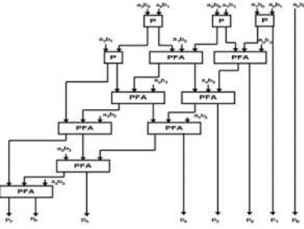
For 4 bit multiplication totally there are 3 stages of partial product reduction. If there are p rows of partial products,rows are passed to the next stage. These rows are summed using fulladders [(3,2) counters] if there are 3 partial products in 1 column and using half adders[ (2,2) counter] if there are 2 partial products in 1 column. The resulting sum and carry of the full adder and half adder are passed on to the next stage. Finally in the last stage Full adders are used to obtain the product. The full adder block is replaced by the Peres full adder. Similarly, half adder block is replaced by Peres half adder block.Figure.6 shows the 4x4 reversible Wallace multiplier.
P – Peres reversible gate as half adder, PFA – Peres reversible gate as full adder
Figure.6 Reversible Wallace multiplier
B.2 Reversible Dadda multiplier:
In the Dadda multiplication,[Figure.7] the first stage consists of N2 AND gates, forming the partial products. The successive reduction levels involves the Peres full adder and Peres half adder blocks leading to the resultant product.
P – Peres reversible gate as half adder, PFA – Peres reversible gate as full adder
Figure.7Reversible Dadda multiplier
Among the adders discussed in the conventional design, Carry lookahead adder realization in reversible logic gives better result when compared to the Ripple carry adder, Carry select adder and Carry save adder. In the adder blocks, the full adder is replaced by Peres gate. In CLA, the generate and propagate block is replaced by the Peres gate and Toffoli reversible gates, since addition and multiplication operation are present in the corresponding reversible gates. The Figure.10 shows the generate propagate logic (GPL) realization in Carry look ahead adder. The inputs to the GPL are a, b and c and the outputs are p,q,c1.
Figure.8 Generate propagate logic in CLA
Extension
The Vedic Multiplier and the Reversible Logic Gates has Designed A Vedic multiplier is composed by utilizing Urdhava Triyagbhayam sutra and the snake configuration is finished by utilizing reversible rationale entryway. Reversible rationales are likewise the crucial necessity for the developing field of Quantum processing. By using vedic we can decrease area and delay.
IV RESULTS
PROPOSED RESULTS Simulation result:
SYNTHESIS RESULTS:
RTL SCHEMATIC:
DESIGN SUMMARY:
TIMING REPORT:
EXTENSION RESULTS:
SIMULATION RESULT:
SYNTHESIS RESULTS:
RTL SCHEMATIC:
TECHNOLOGY SCHEMATIC:
DESIGN SUMMARY:
COMPARISON TABLE
V. CONCLUSION
In this paper, low power reversible FIR filter architecture is proposed. In the proposed method the input data samples and filter coefficients are given as input to the multipliers and adders designed using reversible logic gates. The proposed scheme is compared with the FIR filter realized using normal multipliers and adders and the simulation results, shows that the proposed FIR filter designed using reversible Wallace multiplier and carry lookahead adder The
technique can be used in phonetic signal processing system. The proposed work can be extended to adaptive filter.
REFERENCES
[1] Hunsoo Choo, Khurram Muhammad, and Kaushik Roy, “Two’s Complement Computation Sharing Multiplier and Its Applications to High Performance DFE,” IEEE Transactions On Signal Processing, Vol. 51, No. 2, Feb. 2003.
[2] Richard Hartley, “Optimization Of Canonic Signed Digit Multipliers For Filter Design,” IEEE International Sympoisum on Circuits and Systems, Vol. 4, Jun 1991.
[3] C.R.Baugh and B.A. Wooley, “A two’s complement parallel array multiplication algorithm,” IEEE Trans. On Computers, vol.22, pp. 1045-1047, 1973.
[4] K.A.C.Bickerstaff, E.E.Swartzlander Jr., and M.J.Schulte, “Analysis of column compression multipliers,” 15th IEEE Symp. On Computer Architecture, pp.33-39, 2001.
[5] C.S.Wallace, “A suggestion for a fast multiplier,” IEEE Trans. On Computers, vol. 13, pp. 14-17, 1964.
[6] E.E. Swartzlander Jr., “Merged arithmetic,” vol.29, pp. 946-950, 1980.
[7] S. White, “Applications of Distributed Arithmetic to Digital Signal Processing: A Tutorial Review,” IEEE ASSP Magazine, July 1989, pp. 4 –19.