Impact of Doping in Gate All Around
Nanowire TFET
Praveen C S
1, Ajith Ravindran
2, Shajimon K John
3, Arathy Varghese
4and Ancy P Mani
5PG Scholar, Dept. of ECE, SAINTGITS College of Engineering, Kottayam, Kerala, India1 Asst. Professor, Dept. of ECE, SAINTGITS College of Engineering, Kottayam, Kerala, India2
Professor, Dept. of ECE, SAINTGITS College of Engineering, Kottayam, Kerala, India3 PG Scholar, Dept. of ECE, SAINTGITS College of Engineering, Kottayam, Kerala, India4 PG Scholar, Dept. of ECE, SAINTGITS College of Engineering, Kottayam, Kerala, India5
ABSTRACT:The serious thermal management crisis in next generation digital systems due to power dissipation boom are limited by the reduction of supply voltage. Transistors with lower Subthreshold Slopes (SS) are needed for low power systems. Recent years Tunnel Field Effect Transistors (TFET) are good alternatives for the existing MOSFET to cope up with the continuous scaling down of device dimensions. TFETs have reduced Short Channel Effects (SCE), low OFF current (IOFF) and small SS. Majordrawback of TFETs are their considerably low ON current (ION). The
simplest solution to this problem is a Double Gate (DG) instead of a Single Gate (SG) structure, which will provide ION
improvement. A Gate All Around (GAA) structure is the ultimate solution for improvement of IOFF, and ION/IOFF
current ratio due to its excellent gate coupling. In this paper a GAA nanowire TFET with a channel length of 32 nm having high ION/IOFF ratio is modelled.
KEYWORDS: Steep SS, Band To Band Tunneling, Tunnel FET, Low IOFF, GAA structure.
I.INTRODUCTION
Semiconductor devices are extensively used in all aspects of our life since the invention of the first transistor in early 1960‟s. The revolution of Complementary Metal Oxide Semiconductor (CMOS) technology has been the heart of electronics industry Metal Oxide Semiconductor Field Effect Transistor (MOSFET) device scaling plays an important role in the rapid development of the semiconductor industry. Device scaling allows for more devices and/or functions to be integrated into a single chip with a given silicon area. The transistor gate length has been reduced from 10µm in 1970s to 10 nm in 2015.Co-founder of Intel cooperation, Gordon Moore, made an observation in 1965 which is now known as the “Moore‟s Law”, which states that the number of transistors being integrated into ICs will increase exponentially, doubling every 2 years [1]. The number of transistors in a single IC has increased by more than 6 orders of magnitude over the last 40 years. In order to support the voltage scaling requirement and to reduce the power consumption, new device concepts that can overcome the thermal limit of 60 mV/decade are required.
A device with steeper SS would have its IDS modulated over orders of magnitude with a smaller change in VGS. For the
same VDD, a device with a smaller SS would achieve a lower IOFF for a given ION. Both dynamic power and standby
II.
LITERATURE REVIEWL. Esaki discovered the principle of BTBT in 1957 [2] and the first gated p-i-n structure was proposed in 1978, the interest in the first results on TFETs was limited [3]. There was a rapid change after W. Hansch and I. Eisele et al. started to investigate the TFET in 2000 and in 2004 J. Appenzeller et al. found out that the TFET might provide an useful means to overcome the 60 mV/dec switching limit of the existing MOSFET technology. Various research groups started the extensive study of Tunnel FETs after these successful initial results.
While Appenzeller‟s results were obtained with carbon-nanotube FETs, the adoption of the operating principle to silicon FETs seems to be more attractive because the mature silicon technology could offer a straight route to industrial application. Therefore, recent experiments focus on silicon and germanium [4]. Furthermore, C. Hu proposed a slightly modified TFET structure, which exploits the vertical electric field to create a tunnel junction. To answer the question how the TFET could overcome the 60 mV/dec switching-limit of the MOSFET, the following section introduces its principle of operation.
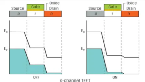
TFET structure is similar to MOSFET, but with opposite type doping in Source and Drain. The simplest TFET is a gated P-i-N diode where the source and drain are highly doped with the gate controlling the band-to-band tunneling between the i-channel region and the P+ or N+ region by way of energy band bending in the i-channel region [5]. Fig 2.1 shows an N-type P-i-N structure TFET. The gate induces an N+ channel to form at the surface of the intrinsic channel region in this case and causes a P+/N+ junction to form at the source to channel interface [14].
Fig. 1 P-i-N TFET structure
TFETs make use of BTBT, which occurs as Zener tunnelling, when a p+/n+ junction is under reverse bias, forming a narrow energy barrier and large electric field as shown in Fig 2.2(b). With available electrons in the valence band on the source side and an empty state in the conduction band on the drain side, the electron can tunnel through the barrier resulting in Zener current flow and the ON-state operation of the TFET.
Fig. 2 OFF-state (a) and ON-state (b) energy band diagrams of TFET [6].
To be analogous to the MOSFET, in an NTFET the source is the P-region and acts as the source of electrons. The channel is the gated intrinsic region and the drain is the N-region. This allows for the same voltage conventions to be used as in an NMOSFET[7]. When there is no applied VGS, a wide barrier exists at the source-channel junction, that is
intrinsic region are pushed down creating a channel that begins to appear N-type [8]. As VGSis further increased the
energy barrier is reduced until the tunnelling probability increases to the point where there is a significant current flow as shown in Fig. 2.2(b). Conversely to the NTFET, the source in the PTFET is the N-region which allows injection of holes into the channel. As in the PMOSFET, negative gate and drain voltages are used to turn on PTFET.
III.GATE ALL AROUND TFET
InA good alternative to improve IONis to achieve better electrostatic coupling by improving the gate-channel geometry
using multi-gate devices such as e.g.: the planar double gate [9], FinFET [10], triple gate [11], and a gate-all-around nanowire structure [12], all being fabricated with either bulk or SOI technology. Enhanced tunneling probability and a boom in ION are the major advantages of GAA structure.In GAA the silicon channel is completely surrounded by
metallic gate. With the advancements in CMOS applications, GAA transistors are being considered as promising candidate due to excellent gate to channel coupling, highly integrable in circuit functionality and compatibility with existing CMOS technology. Process integration of TFET with GAA structure will increase on-chip devise density and will show good gate controllability. Fig. 3.1 depicts schematics of several device cross sections, viewed in the direction of the current flow: a planar SOIFET, a double-gate finFET, and a GAA Nanowire FET. Vertical GAA silicon nanowire FET is already been fabricated by the nano electronic group at institute of microelectronics, and has shown improved performance compared to planar counterparts [15].
Fig. 3 Progression of device structure from conventional single gate planar device to fully GAA structure.
Surround gate structure allows more channel width per unit area of silicon, which leads to an increase of the drive current per unit area. Moreover, for elimination of sub-surface leakage path between the source and drain, this structure utilizes a very thin body and thereby have better gate control,suspension of SCEs, extremely superior short channel immunity with SS ~ 60mV/decade of ION and high ION/IOFF ratio.
Fig. 4 Schematic diagram of gate all around TFET.
ON current of GAATFET is given by Praveen et. al. [16] as,
Idt VGS, VDS = a. f. E. Vtw. e−b/E (3.1)
The parameters a and b are given by,
a =W .TCH.q3
8π2ℏ2
2mr∗
b =4 2mr
∗Eg3
3qℏ (3.3)
Where mr *
= (1/me *
+ 1/mh *
)-1 is the reduced effective mass, which is the sum of the reciprocal of the electron, me *
, and hole, mh*, effective masses. For normalization mr*is multiplied by the electron rest mass m0 = 9.11 x 10⁻³¹. Egis the
semiconductor band gap (1.1eV for Si, 0.35eV for InAs, etc.), ħ = 1.05 x 10⁻³⁴is the reduced Planck‟s constant, TCH is
channel thickness and q = 1.6 x 10⁻¹⁹ is elementary charge.
IV. RESULTS AND DISCUSSIONS
A gate all around NTFET with channel length 32 nanometer is modelled with variable source, channel and drain doping. HfO2 high-k dielectric is used as the gate dielectric with Effective Oxide Thickness (EOT) = 2 nm. Impact of
Doping on GAATFET are studied and verified.
4.1 Impact of Source Doping
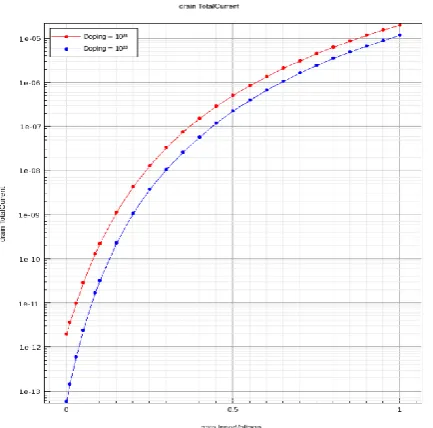
The source-to-channel doping must be heavy and abrupt to maximize on-current in the TFET. Higher values of draing doping of the order of 1020 etc. are used. Drain Induced Barrier Lowering (DIBL) is defined herein as the shift in gate voltage corresponding to an off-state leakage current of 10 pA/μm induced by a 1-Volt change in drain voltage, in units of mV/V. For high values of Source doping, the device turns ON with point tunneling, which is more susceptible to the influence of the drain bias, because it affects the channel potential. Reverse-bias P/N-junction diode leakage increases with decreasing Source doping, and becomes dominant at low values of Source doping. A lower Source doping, increases the sensitivity of drain current on the drain bias, though with a lower net change in DIBL when compared to a high Source doping.
Fig. 5 Log ID - VGSplot for source doping 1020 and 1021 cm-3
Source doping has a direct impact on both ON and OFF currents, heavy doping in the source region and abrupt source-channel doping profile will improve ON current. Applied VDS is 0.1V, VGS is varied from 0V to 1V in steps of 0.1V. ID
- VGScurve for source doping values of 1020 cm-3 and 1021 cm-3 are shown in figure 4.1, improvement of ON current is
4.2 Impact of Drain Doping
Drain doping needs to be carefully designed in order to optimize TFET device performances. When the drain and source doping are equal, the Tunnel FET has undesirable ambipolar characteristics. Thus, lower drain doping is desirable to suppress the ambipolarity and also to reduce the OFF state leakage current.
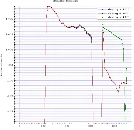
Fig. 6 Logarithmic plot of BTBT for 3 different drain doping
The plot shows the variation in band to band tunneling rate for drain doping concentrations 1018, 1019 ad 1020 cm-3. From the graph it is seen that the source side band to band tunneling rate is unaffected by the drain side doping. For a doping concentration of 1018 cm-3, the drain side BTBT is negligible during ON condition (blue line in figure 4.2), but when it comes to doping concentration of 1019 cm-3, we can see that the drain side BTBT contributing to off current is having a higher value (brown line in figure 4.2). and finally in the case of doping concentration of 1020 cm-3, which is equal to source doping, drain side BTBT becomes comparable to source side BTBT (green line in figure 4.2) which calls off for very high OFF current, resulting is ambipolarity.
4.3 Impact of Channel Doping
Fig. 6 ON and OFF state band diagram for a channel doping of 1015 cm-3and 1016 cm-3
As TFETs work on the principle of BTBT, like BTBT generation rate; band diagrams can also be used for comparison. It evident from the band diagrams in figure 4.3 and 4.4 that large tunneling window is present for an N-type channel with a light doping of 1016. A larger tunneling window undoubtedly yields higher ON current.
4.4 Optimum doping profile of GAATFET
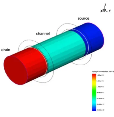
Optimum value of source drain and channel doping concentrations are shown in figure 4.5.The optimum values of source, channel and drain doping are 1x1020cm-3, 1x1016cm-3and 1x1018cm-3respectively. The gate metal and oxide are removed intentionally from this diagram for clear visibility of channel doping.
Fig. 7 Optimum doping profile of GAATFET.
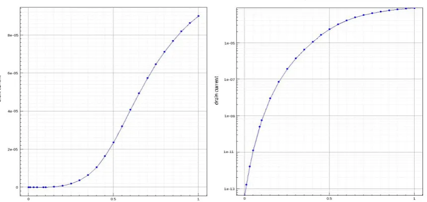
Fig. 8 Normal and Log scale ID-VGS characteristics of optimum doped GAATFET
V.CONCLUSION
TFETs proved themselves to be the best replacement for existingMOSFET technology due to there reduced leakage current. Along with the ultra low OFF current we are getting very low ON current also. An effective solution include structural changes; a GAA structure instead of a single gate structure will provide improvement in ION and also IOFF.A
gate all around Tunnel FET is modelled with optimum source channel and drain doping 1x1020cm-3, 1x1016cm-3and 1x1018cm-3respectively, for attaining high ION/IOFF ratio. ION/IOFFratio of the order of 109 is obtained by doping with the
optimum values in the gate all around structure. Fabrication study is much necessary for the best results. Very stringent process requirement and variation control are required in order to fabricate and characterize such devices successfully.
REFERENCES
[1]. Moore, Gordon E. "Cramming more components onto integrated circuits, Reprinted from Electronics, volume 38, number 8, April 19, 1965, pp. 114 ff." IEEE Solid-State Circuits Newsletter 3, no. 20, pp. 33-35, 2006.
[2]. L. Esaki, “New Phenomenon in Narrow Germanium p - n Junctions”, Physical Review, vol. 109, pp. 603-604, 1958.
[3]. S. Banerjee, W. Richardson, J. Coleman and A. Chatterjee, “A new three-terminal tunnel device,” IEEE Electron Device Letters, vol. 8, pp. 347-349, 1987.
[4]. K.K. Bhuwalka, J. Schulze, I. Eisele, “Scaling the Vertical Tunnel FET with Tunnel bandgap Modulation and Gate Workfunction Engineering,” IEEE Trans. Electron Devices, vol. 52, no. 5, pp. 909-917, 2005.
[5]. W. M. Reddick and G. A. Amaratunga, "Silicon surface tunnel transistor," Applied Physics Letters, vol. 67, no. 4, July 1995, pp. 494-496. [6]. Alan Seabaugh, The Tunneling Transistor,IEEE Spectrum, 30 Sep 2013.
[7]. E. O. Kane, "Theory of Tunneling," Journal of Applied Physics, vol. 32, p.83, 1961.
[8]. S. M. Sze and K. K. Ng, Physics of Semiconductor Device, 3rd Edition, John Wiley & Sons, Inc., 2007, pp. 422-425.
[9]. D. Hisamoto, Wen-Chin Lee, J. Kedzierski, H. Takeuchi, K. Asano, C. Kuo, E. Anderson, Tsu-Jae King, J. Bokor, and Chenming Hu, “FinFET-a self-aligned double-gateMOSFET scalable to 20 nm”, Electron Devices, IEEE Transactions on, vol 47(12), pp. 2320 – 2325, 2000. [10]. Xuejue Huang, Wen-Chin Lee, Charles Kuo, D. Hisamoto, Leland Chang, J. Kedzierski, E. Anderson, H. Takeuchi, Yang-Kyu Choi, K. Asano,
V. Subramanian, Tsu-Jae King, J. Bokor, and Chenming Hu, “Sub 50-nmFinFET: PMOS”, In Electron DevicesMeeting, 1999. IEDM Technical Digest. International, pp. 67 –70, 1999.
[11]. B. Doyle, B. Boyanov, S. Datta, M. Doczy, S. Hareland, B. Jin, J. Kavalieros, T. Linton, R. Rios, and R. Chau, “Tri-gate fully-depleted CMOS transistors: fabrication, design and layout”, In VLSI Technology, 2003. Digest of Technical Papers. 2003 Symposiumon, pp. 133 – 134, 2003. [12]. J.P. Colinge, M.H. Gao, A. Romano-Rodriguez, H.Maes, and C. Claeys, “Siliconon- insulator „gate-all-around device‟ ”, In Electron
DevicesMeeting, 1990. IEDM ‟90. Technical Digest., International, pp. 595 –598, 1990.
[13]. J. Appenzeller, J. Knoch, M.T. Bjork, H. Riel, H. Schmid and W. Riess, “Towards nanowire electronics,” IEEE Trans. On Electron Devices, vol. 55, pp. 2827, 2008.
[14]. S. Banerjee, W. Richardson, J. Coleman and A. Chatterjee, “A new three-terminal tunnel device,” IEEE Electron Device Letters, vol. 8, pp. 347-349, 1987.
[16]. Praveen C S, Ajith Ravindran and Arathy Varghese. Article: Analysis of GAA Tunnel FET using MATLAB. IJCA Proceedings on International Conference on Emerging Trends in Technology and Applied Sciences ICETTAS 2015(1), pp. 30-35, 2015.
BIOGRAPHY
Mr. Praveen C S
Pursuing M.Tech Degree in VLSI & Embedded Systems from Mathma Gandhi University, Kottayam, India. Received B.Tech. Degree in Electronics and Communication Engineering from Mathma Gandhi University, Kottayam, India, in 2012. His areas of interests include device modeling, low power design of VLSI circuits.
Mr. Ajith Ravindran
Received his B.Tech and M.Tech. Degrees in Electronics and Communication Engineering from Mathma Gandhi University, Kottayam, India, in 2010 and 2012 respectively. He is working as an Assistant Professor in the Department of ECE, Saintgits College of Engineering, Kottayam, since 2012. His current research interests include low-power VLSI systems, and device modeling.
Prof. Shajimon K John
Received his B.Tech degree in Electronics and Communication Engineering from Bharathiyar University and M.Tech. Degrees in Applied Electronics from Anna University, Chennai, India, He has been with the Department of ECE, Saintgits College of Engineering, Kottayam, since 2005. He is currently working there as a Professor. His current research interests include VLSI systems, and Signal processing.
Ms. Arathy Varghese
Pursuing M.Tech Degree in VLSI & Embedded Systems from Mathma Gandhi University, Kottayam, India. Received B.Tech. Degree in Electronics and communication Engineering from Kerala University, Trivandrum, India, in 2013. Her areas of interests include device modeling and Digital design of VLSI circuits.
Ms. Ancy P Mani