Design of Non-Volatile Memory Based On
Improved Writing Circuit STT-MRAM
Technique
D.Ramya
1, P.Balaganesh
2PG Scholar, M.E VLSI DESIGN, Sri Vidya College of Engineering and Technology, Tamilnadu, India1
Assistant Professor, Department of ECE, Sri Vidya College of Engineering and Technology, Tamilnadu, India2
ABSTRACT: Spin-transfer torque magnetic RAM (STT-MRAM) is a one of the memory application for next generation. It has many attractive features like high density and low leakage. However, it comes with high write power due to large current required to achieve fast switching speed. The STT-MRAM target mainly to replace SRAM or DRAM. It is used as a working memory in the cache, high access speed is one of the most critical performance. The objective of our project is to contribute one such storage device by making NVM based on Spin Transfer Torque Magnetic Random Access Memory (STT-MRAM). STT-MRAM based on resistive switching mechanism. In this proposed work we are reducing power and area. The NVM circuit has been implemented using Tanner Tools using 220nm technology and the responses are obtained. In this paper achieve the low power and sensing the each bit for reading.
KEYWORDS:MRAM, CMOS, Resistive Switching, Magnetic Tunnel Junction, Writing/Reading Circuit
I. INTRODUCTION
Memory system is the heart of the processor. On-chip memory occupies a more portion of the over-all processor in a system. The last few years, advance improvements in memory density; this has also resulted in an increase of power dissipations, Energy for data transfer and read/write delay [2].
Volatile memory to non-volatile memory, is computer memory that requires power to maintain the stored information; it retains its contents while powered, but when power is interrupted stored data is immediately lost. Volatile memory has several uses, as a RAM drive. Non-volatile memory is typically used for the task of secondary storage, or long-term persistent storage. However, most forms of non-volatile memory have limitations that make them unsuitable for use as primary storage. Non-volatile memory costs are more. The memory is efficiently used for the processor. Computational complexity of memory usage becomes an important problem for all devices [8].
The development of new generation non-volatile memories, such as Phase Change Memories (PCMs) and Resistive-RAMs, calls for accurate and controllable programming pulses, which are fundamental to adequately characterize the memory cell [3].Magnetic tunnel junction based logic has a great potential of the non-volatility, unlimited endurance, CMOS compatibility, and fast switching speed of the MTJ devices. MRAM cells integrate a magnetic tunnel junction (MTJ) consisting of a thin insulating barrier (i.e.,MgO) separating two ferromagnetic (FM) layers. SPIN-TRANSFER TORQUE (STT) magnetic tunnel junction (STT-MTJ) technology combines the advantages of CMOS compatibility, high speed, high density, unlimited endurance, and scalability, fast read/write [1],[3].
Pandian Saraswathi Yadav Engineering College, Arasanoor, Sivagangai, Tamilnadu, India
In this paper presents a design of MRAM using STT-MRAM technique to improve writing/reading speed and sensing the data for the operation. Spin Transfer Torque Magnetic RAM (STT-MRAM) promises low power, great miniaturization prospective and easy integration with CMOS process.
II. SYSTEM ARCHITECTURE
The MRAM design includes magnetic flip flop design, precharge sensing amplifier and writing/reading circuit. Fig 1.shows the block diagram of MRAM design.
.
Fig. 1 Block diagram of MRAM design
A. Magnetic Random Access Memory
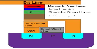
Unlike conventional RAM chip technologies, data in MRAM is not stored as electric charge or current flows, but by magnetic storage elements. The elements are formed from two ferromagnetic plates, each of which can hold a magnetic field, separated by a thin insulating layer. One of the two plates is a permanent magnet set to a particular polarity; the other plate's field can be changed to match that of an external field to store memory. This configuration is known as a spin valve and is the simplest structure for an MRAM bit [5].
Fig. 2 Simplified structure of MRAM cell
In this structure have three layer free layer, fixed layer and tunnel barrier. The fixed layer is a permanent magnet and the free layer is magnetic effect at the current given time. The potential arrangements include "Thermal Assisted Switching" (TAS-MRAM), which briefly heats up (reminiscent of phase-change memory) the magnetic tunnel junctions during the write process and keeps the MTJs stable at a colder temperature the rest of the time; and "vertical
MRAM
Magnetic Flip Flop Design
Input Data
Precharge Sensing Amplifier
Writing/Reading circuit
transport MRAM" (VMRAM), which uses current through a vertical column to change magnetic orientation, a geometric arrangement that reduces the write disturb problem and so can be used at higher density [20].
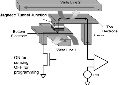
Fig. 3 MRAM cell structure, showing the sense path
The MRAM is composed of a thin oxide pass transistor, a single MTJ, top and bottom sense electrodes, and two orthogonal program lines, as shown in Fig. 3. A connection is made from the base contact of the bit to ground through a via stack connected to an isolation transistor in the underlying CMOS. Flowing current through the program conductors produces the magnetic fields necessary to switch the state of the bit. In this architecture, the program lines are physically separated from the MTJ, which reduces the parasitic delay.
The MTJ is composed of a pinned magnetic layer, a tunnel barrier, and a free magnetic layer. Electrons spin polarized by the magnetic layers traverse the tunnel barrier. A parallel alignment of the free layer with respect to the pinned layer results in a low resistance state, while an antiparallel alignment results in a high resistance state. The sense circuitry is composed of a thin oxide pass transistor, which is electrically connected to the MTJ by the bottom and top electrode conductors. In order to read the bit, the isolation transistor is turned on, and a small current of about 10 A (depending on the resistance of the material, size of the bit, and desired bias condition) is passed through the bit to sense the resistance. The MRAM module is inserted late inthe CMOS process flow, making the MRAM module and the CMOS independent from one another [6].
B. Magnetic Flip Flop Design
Magnetic flip-flop (MFF) design libraries has been developed using a unique MRAM process. This is comparable to that of a normal CMOS DFF. An MFF test chip was fabricated with the process. Which helps to reduce the power dissipation .Which performs; possible magnetic data store and restore operations. Non-volatile (of computer memory) having the property of retaining data when electrical power fails or is turned off. A flip-flop or latch is a circuit that has two stable states and can be used to store state information [4].
Flip-flops and latches are used as data storage elements. Such data storage can be used for storage of state, and such a circuit is described as sequential logic. When used in a finite-state machine, the output and next state depend not only on its current input, but also on its current state (and hence, previous inputs). It can also be used for counting of pulses, and for synchronizing variably-timed input signals to some reference timing signal [10].
Pandian Saraswathi Yadav Engineering College, Arasanoor, Sivagangai, Tamilnadu, India
C. Precharge Sensing Amplifier
Fig. 4 Pre-Charge Sense Amplifier for STT-RAM
The PCSA for spin transfer torque random access memory which allows lower the current and shorting the delay. These circuits consist of two sub circuit one is precharge sub-circuit and another one is discharge sub-circuit. It operates at two phases; first apply input 0 PMOS transistor is ON to get a output for sensing data. And then apply input 1 the NMOS transistor is ON to get a sensing output. The pair of inverters acts like a amplifier. Using the resistance at the circuit it sensing the data at lower state and higher state. The resistance is higher state it sense the data to through the output [16].
A sensing amplifier is an amplifier that senses the output on the bit lines and amplifies it. The sense amplifier that is used in the design of sensing the write/reading data completely. This approach presents numerous advantages over it single ended counterpart. One of the advantage is the common mode rejection. It means that such an amplifier rejects noise that is equally injected in both inputs [2].
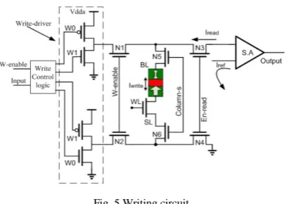
D. Writing/Reading Circuit
Fig. 5 Writing circuit
obtain smaller resistance, and one high supply voltage in writing branch is used to generate a higher current, where
Vdda is higher than the logic voltage V dd. The calculated switching energy of one switching operation is up to 36 pJ/bit, which makes the writing power consumption high.
In the reading branch, there are also column selected transistors (N3 and N4). As these transistors are used to select one column, their size can be small, which makes total resistance large and reading current low. According to (1)–(3), this low reading current can reduce significantly the read disturbance probability [20]. The added logic increases the number of transistors in the proposed circuit. However, the total area is not larger than that of the conventional circuit, as the transistor size in the conventional circuit is larger to obtain small resistance in the writing circuit.
The sensing operation suffers from high sensitivity to process voltage temperature variations. Although the writing circuit with low supply voltage could further decrease power and area consumption, the Monte Carlo statistical analysis of sensing output is worse due to the high resistance in sensing circuit. To improve the reliability of reading circuit, we propose another novel circuit, shows Fig as shown in Fig. 6.
Fig. 6 Reading circuit
The column selected transistor is shifted to the post of SA, and the output of SA is outputted by the column selected transistor. The reduction of transistor number in sensing circuit decreases the sensitivity to process variations. Unfortunately, each column of cellarray needs one SA, which results in area overhead. For the 16 kb STT-MRAM with 256 rows and 64 columns array, the area overhead is ∼33 μm2, which is 10% of the storage array. This area overhead can be negligible because the sensing circuit is often widely shared by many elements of memory array.
III. PROPOSED IMPROVED ENABLE WRITING CIRCUIT USING STT-MRAM TECHNIQUE
Pandian Saraswathi Yadav Engineering College, Arasanoor, Sivagangai, Tamilnadu, India
The above figure consists of RSM, Sensing amplifier, Read and write circuit. RSM act as a port at input and output. Sensing amplifier is used to sense the read and write signal also sense switching activities of turn on and off. The circuit is active write the data into the memory. And then reading circuit is activated to read the given data. In this proposed circuit see the reading operation when the system powered off.
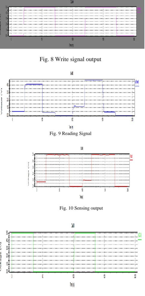
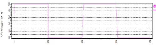
Fig. 8 Write signal output
Fig. 9 Reading Signal
Fig. 10 Sensing output
Fig. 12 Input Data
The above graphs are obtained from the simulation of the NVM cell STT-MRAM realization. The input 1010 given to the circuit as shown in fig 12. Give the clock signal to activate the circuit for read and write as shown in fig 11. Activate write circuit to sense the input to write the data as shown in fig 10. And then read the data as shown in fig 9.Fig 8 is the sensing output. It uses to sense the read signal. When power off the system a sensing circuit sense the read signal to continue read the data.
V. CONCLUSION
In this paper, design of STT-MRAM based on Spin transfer torque and Magnetic flip-flop is proposed in our work with CMOS technology, In the e design that was based on self-gating power gate mechanism, our proposed design provides promising result than existing system. Our work concentrated on reduction of power and reduced delay, and also area efficiency, thus from the overall parameters we have achieved better performance than the existing design of Flip-flop. For this design held in CMOS design methodology and we have used Tanner EDA 15.11 as simulation tool to show the performance analysis.
REFERENCES
[1] Nam Sung Kim, Todd Austin David Blaauw, (2003) “Leakage Current: Moore‟s Law Meets Static Power”IEEE Transactions.
[2] Weisheng Zhao, Mathieu Moreau, (2014) “Synchronous Non-Volatile Logic Gate Design Based on Resistive Switching Memories”IEEE Transactions, Vol 61, No.2, February.
[3] Claude Chappert, Albert Fert,(2007) “The emergence of spin electronics in data storage”IEEE Transactions. [4] Weisheng Zhao, Eric Belhaire, (2007) “New non-volatile logic basedon spin-MTJ”IEEE Transactions.
[5] C.J. Lin, S.H. Kang, (2009) “45nm Low Power CMOS Logic Compatible Embedded STT MRAM Utilizing a Reverse-Connection 1T/1MTJ Cell”IEEE Transactions. [6] B. N. Engel, J. Åkerman,(2005) “A 4-Mb Toggle MRAM Based on a Novel Bit andSwitching Method”IEEE Transactions, Vol. 41, No. 1, January.
[7] W.S. Zhao, Y. Zhang, (2012) “Failure and reliability analysis of STT-MRAM”IEEE Transactions.
[8] Lee, H.Y Chen, (2010) “Low-Power and Nanosecond Switching in Robust Hafnium Oxide Resistive Memory with a Thin Ti Cap”IEEE Transaction,Vol. 31, No. 1, January.
[9] R. Nara, N. Togawa, (2005) “Multi-layer cross-point binary oxide resistive memory (OxRRAM) for post-NAND storage application”IEEE Transactions. [10] FransTheeuwen, Eric Seelen, (2007) “Phase-change materials for rewriteable data storage” IEEE Transactions.
[11] Koji Ando, SumioIkegawa, (2011) “Pulser gating: A clock gating of pulsed-latch circuits”IEEE Transactions.
[12] KazuteruNamba, Fabrizio Lombard, (2013) “Extending Non-Volatile Operation to DRAM Cells”IEEE Transactions, November.
[13] Erika Covi, Alessandro Cabrini, (2014) “On-Wafer Analog Pulse Generator for Fast Characterization and Parametric Test of Resistive Switching Memories” IEEE Transactions,Vol.27, No.2, May.
[14] HiwaMahmoudi, Thomas Windbacher, (2013) “Reliability Analysis and Comparison of Implication and ReprogrammableLogic Gates in Magnetic Tunnel Junction Logic Circuits”IEEE Transactions, Vol.49, No.12, December.
[15] An Chen, (2014) “Area and Thickness Scaling of Forming Voltage of Resistive Switching Memories”IEEE Transactions, Vol.35, No.1, January.
[16] Li Zhang,Weisheng Zhao, (2014)“A 16 Kb Spin-Transfer Torque Random Access Memory With Self-Enable Switching and Precharge Sensing Schemes” IEEE Transactions, Vol.50, No.4, April.
[17] Liye Wang ,Shulong Li, (2005)“A Pure Logic CMOS Based Low Power Non-Volatile Random Access Memory”IEEE Transactions.
[18] Bin Gao,Bing Chen , (2.13)“A Novel Defect-Engineering-Based Implementation for High-Performance Multilevel Data Storage in Resistive Switching Memory”IEEE Transactions, Vol.60, No.4, April.
[19] Kejie Huang, YajunHa, (2014)“A Low Active Leakage and High Reliability Phase Change Memory (PCM) Based Non-Volatile FPGA Storage Element”IEEE Transactions,Vol.61, No.9, September.