Static and Dynamic TSEPs of SiC and GaN Transistors
Siwei Zhu, Asad Fayyaz, Alberto Castellazzi
Power Electronics, Machines and Control Group, University of Nottingham, UK Phone: +44-115-951-5568, e-mail: [email protected]
Abstract— This paper investigates the static and dynamic
temperature sensitive electrical parameters (TSEPs) for both SiC and GaN transistors. It is shown that both the qualitative and quantitative temperature characteristics of these parameters are various when different type of transistors are concerned. This finding can be used to select the most appropriate temperature sensitive parameter for the device under specific situation. In this paper, two types of transistors, SiC SCT2080KE MOSFET and GaN PGA26E19BA HEMT are evaluated and compared in terms of six TSEPs, including source-drain reverse bias voltage (VSD), static on-resistance (RDS,ON), gate threshold voltage (VGS(TH)), transconductance (gm), dIDS/dt switching transients and gate current (IG). Then, these TSEPs are compared using four criteria: temperature sensitivity, linearity, material and the capability of on-line temperature monitoring.
Keywords- SiC MOSFET, GaN HEMT, TSEPs, on-line temperature monitoring.
I. INTRODUCTION
The on-line junction temperature of the device under operating condition has a significant effect on the performance, robustness and reliability of the system. Therefore, the ability to monitor the real-time junction temperature is a key in the design of reliable power system. In addition, it can be also used as a damage indicator and prolong the lifetime of the system. Recently, several temperature monitoring techniques are proposed [1]. Among of them, integrating temperature and current sensor in the chip is the most effective and direct way of estimating the condition of the device. However, for the generic power devices, this method is not commonly available [2]. Considering the packaged commercial devices and interfacing within a power system, temperature sensitive electrical parameters (TSEPs) could be an alternative method of estimating the junction temperature of the device [3]. It is an indirect temperature measurement method which is based on the temperature dependency of electrical parameters.
In this paper, a N-channel 1200V – 40A rated MOSFET (SCT2080KE) and a p-gate type 600V – 15A rated HEMT(PGA26E19BA) are investigated in terms of six TSPEs: source-drain reverse bias voltage (VSD), static on-resistance (RDS,ON), gate threshold voltage (VGS(TH)), transconductance (gm) dIDS/dt switching transients and gate current (IG). Then, these TSEPs are compared using 4 criteria: temperature sensitivity, linearity, material and the capability of on-line temperature measurement.
II. METHODOLOGY
The calibration is an important procedure in the temperature measurement of the semiconductor device using TSPEs, where the relationship between TSEPs and device temperature are determined [3]. The system temperature is known and fixed by external source, such as a hot plate. Then, the values of electrical parameter as a function of temperature can be obtained. During the calibration, concerning the self-heating problems, the power dissipation has to be limited at low level to achieve accurate calibration data.
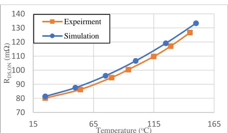
[image:1.612.342.556.434.565.2]In order to find an appropriate test condition where the self-heating is minimized and a relatively high temperature resolution can be achieved. The simulations on the temperature dependencies of different TSEPs are implemented [4]. For example, Fig.1 presents the schematic of PSpice simulation on the temperature dependency of static on-resistance of SCT2080KE MOSFET. The self-heating is minimized while a pronounced temperature effect on the static on-resistance is achieved with 0.1A constant DC drain current and 18V gate source bias voltage, where R1 is used to simulate the cable resistance while R2 is used to simulate the internal gate resistance of the device. The temperature varies from 25 to 150oC with step of 25 oC and the drain voltage is measured using voltage probe with reference to the ground. The static on-resistance can be then calculated using the equation RDS,ON = VDS / IDS. Fig. 2 shows the comparison between the simulation and experiment result in the temperature dependency of static on-resistance of SCT2080KE MOSFET. The slightly temperature mismatch in the experiment is caused by the overshot of the hot plate. However, this error can be negligible since sufficient experiment points are obtained and the temperature ranges from 25 to 150oC approximately. The temperature sensitivity of static on-resistance of simulation is 0.4155 mΩ/oC and that of experiment is 0.3873 mΩ/oC. As a result, the experiment result almost matches with simulation expectation, where the static on-resistance shares a positive relationship with temperature.
Figure 1: PSpice simulation on the temperature dependency of static on-resistance of SCT2080KE MOSFET.
Figure 2: Simulation expectation vs experiment result in temperature dependency of static on-resistance of SCT2080KE MOSFET.
70 80 90 100 110 120 130 140
15 65 115 165
RD
S
,O
N
(m
Ω
)
Temperature (oC) Expeirment
[image:1.612.333.562.593.727.2]III. EXPERIMENT RESULTS
A.TSPEs of SCT2080KE MOSFET
Five TSPEs of a N-channel 1200V – 40A rated MOSFET (SCT2080KE) are analyzed, namely, source-drain reverse bias voltage (VSD), static on-resistance (RDS,ON), gate threshold voltage (VGS(TH)), transconductance (gm), dIDS/dt switching transients. The corresponding simulations are implemented and appropriate test conditions are determined based on the methodology discussed above (chapter II). The temperature varies from 25 to 150 oC in step of 25 oC using hot plate and the values of electrical parameters are obtained as function of temperature through the current or voltage probes.
The temperature dependency of source-drain reverse bias voltage is explored in Fig. 3 under the condition of VGS = 0V and IS = 0.2A. Relatively small Is was chosen to minimize the effect of self-heating. The VSD is inversely proportional to the temperature and shows a good linearity. The calculated temperature sensitivity is 3.765 mV/oC. Fig 4 presents the temperature dependency of static on-resistance. RDS,ON was measured with 0.1A drain bias current at VGS = 18V. Under this test condition, relatively high temperature resolution can be achieved and the self-heating caused by drain-source current is minimized. Consequently, RDS,ON is directly proportional to the temperature and the corresponding temperature sensitivity is 0.3873 mΩ/oC. The temperature characteristic of gate threshold voltage is shown in Fig 5.
VGS(TH) was measured when the drain-source current reached
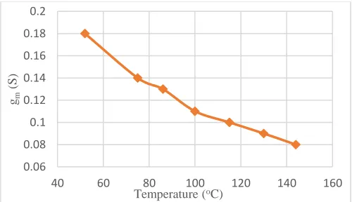
to 4.4mA and this value is based on the SCT2080KE datasheet [5]. A negative temperature coefficient of VGS(TH) is observed and it shares a good linearity with temperature. The estimated temperature sensitivity is 7.045 mV/oC. Fig.6 shows the temperature dependency of transconductance. The transconductance discussed here refers to the change of drain-source current divided by the change of gate-drain-source voltage, gm = ∆IDS / ∆VGS. VGS varies from 15V to 19V at 0.75V drain-source bias voltage. 15V to 19V voltage region was selected to achieve maximum change of IDS and the effect of self-heating was minimized since the value of VGS was limited in a relatively low level. gm decreases linearly with the increasing of temperature and the calculated temperature sensitivity is 0.8 mS/oC. Finally, the temperature characteristic of dI
DS/dt
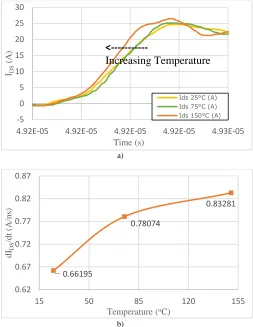
[image:2.612.333.584.39.185.2]switching transient was investigated through the double pulse test. Under the test condition of VDS = 400V, VGS = 18V and 25A drain-source bias current. The rise time and fall time are determined by the time when it is in the range of 10% - 90% of the maximum rated value (2.5A – 22.5A). From Fig. 7, it is found that the switching rate during the turn ON transient increases with temperature and dIDS/dt shares a positive relationship with temperature. The calculated temperature sensitivity is 1.367 (mA/ns) / oC. This is due to the negative temperature coefficient of VGS(TH). The required threshold voltage for higher temperature is reduced and therefore the device is switched on faster. However, the increasing of dIDS/dt switching rate is limited when the temperature is above 100 oC. The possible reason for this is that effect of decrease of VGS(TH) with temperature is compensated by the decrease of channel mobility at high temperature [6-8].
[image:2.612.333.583.223.363.2]Figure 3: Temperature dependency of source-drain reverse bias voltage with VGS= 0V and IS = 0.2A of SCT2080KE MOSFET.
Figure 4: Temperature dependency of static on-resistance with 0.1A drain bias current at VGS = 18V of SCT2080KE MOSFET.
Figure 5: Temperature dependency of gate threshold voltage when IDS =
4.4mA OF SCT2080KE MOSFET.
Figure 6: Temperature dependency of transconductance with VGS varies
from 15 to 19V at 0.75V drain-source bias voltage of SCT2080KE MOSFET.
1.4 1.5 1.6 1.7 1.8 1.9 2 2.1
15 65 115 165
V
sd
(V
)
Temperature (oC)
70 80 90 100 110 120 130
15 65 115 165
RDS,
ON
(m
Ω
)
Temperature (oC)
2 2.2 2.4 2.6 2.8 3 3.2
15 65 115 165
VGS(
T
H)
(V
)
Temperature (oC)
0.06 0.08 0.1 0.12 0.14 0.16 0.18 0.2
40 60 80 100 120 140 160
gm
(S
)
[image:2.612.333.583.401.539.2] [image:2.612.334.584.578.722.2]a)
[image:3.612.49.302.39.366.2]b)
Figure 7: Turn ON transient temperature dependency of SiC SCT2080KE MOSFET: drain-source current vs Temperature, a); change of drain-source
current in time vs Temperature, b).
B. TSEPS of PGA26E19BA HEMT
The interested device is a 600V – 15A rated Gate Injection AlGaN/GaN HEMT, which is based on a GaN-on-Si substrate technology [9-10]. Similar to the SiC device, 6 TSEPs are investigated in consideration of comparison, namely, source-drain reverse bias voltage (VSD), static on-resistance (RDS,ON), gate threshold voltage (VGS(TH)), transconductance (gm), dIDS/dt switching transients and gate current (IG). Based on the methodology explained in chapter II, the simulation models are built and appropriate test condition are determined to achieve good temperature resolutions of TSEPs. The experiment temperature is adjusted using hot plate from 25 oC to 150 oC with step of 25 oC and the values of electrical parameter are obtained as function of temperature using probes.
The temperature characteristic of source-drain reverse bias voltage of PGA26E19BA HEMT is shown in Fig. 8. Under the test condition of VGS = 0V and IS = 1.0A, VSD increases slightly with temperature and the calculated temperature sensitivity is 0.141 mV/oC. A relatively higher temperature resolution can be achieved if the source-drain bias current is set to a large value. However, at that condition, the effect of self-heating is not negligible and would result in an inaccurate experiment result. Fig. 9 presents the temperature dependency of static on-resistance. RDS,ON was measured with IGS = 10mA at 0.1A drain bias current. It is directly proportional to the temperature and has a linear variation with temperature. The estimated temperature sensitivity is 1.064 mΩ/oC. Fig. 10 shows the
temperature characteristic of gate threshold voltage with 2V drain-source bias voltage. The VGS(TH) was measured when the drain current reaches to 0.2mA. A relatively small drain current was selected compared with SiC device since the drain current increases rapidly (0.2mA to 200mA instantaneously) and this can be attributed to the material properties of GaN [9]. It can be observed that VGS(TH) decreases linearly with temperature and the corresponding temperature sensitivity is 1.135 mV/oC. Fig. 11 presents the temperature dependency of transconductance where the VGS varies from 2V to 3V with 1.5V drain-source bias voltage. Under this test condition, the effect of self-heating is small and noticeable changes of IDS were observed. gm is calculated based on the equation gm =
[image:3.612.331.583.416.548.2]∆𝐼𝑑𝑠 ∆𝑉𝑔𝑠 and it is inversely proportional to the temperature. The calculated temperature sensitivity is 6.330 mS/oC.
[image:3.612.335.584.593.724.2]Figure 8: Temperature dependency of source-drain reverse bias voltage when VGS = 0V and IS = 1.0A of PGA26E19BA HEMT.
Figure 9: Temperature dependency of static on-resistance when IGS =
10ma and ID = 0.1A of PGA26E19BA HEMT.
Figure 10: Temperature dependency of gate threshold voltage with 2V drain-source bias voltage when ID = 0.2mA of PGA26E19BA HEMT.
-5 0 5 10 15 20 25 30
4.92E-05 4.92E-05 4.92E-05 4.92E-05 4.93E-05
IDS
(A
)
Time (s)
Ids 25°C (A) Ids 75°C (A) Ids 150°C (A)
<---Increasing Temperature
0.66195
0.78074
0.83281
0.62 0.67 0.72 0.77 0.82 0.87
15 50 85 120 155
dIDS
/d
t
(A
/n
s)
Temperature (oC) 1.5
1.6 1.7 1.8 1.9 2 2.1 2.2 2.3
20 55 90 125 160
V
sd
(V
)
Temperature (oC)
120 170 220 270 320
15 65 115 165
RDS,
ON
(m
Ω
)
Temperature (oC)
1.22 1.26 1.3 1.34 1.38 1.42
15 45 75 105 135 165
VGS(
T
H)
(V
)
Figure 11: Temperature dependency of transconductance with VGS from 2V to 3V at 1.5V drain-source bias voltage of PGA26E19BA HEMT.
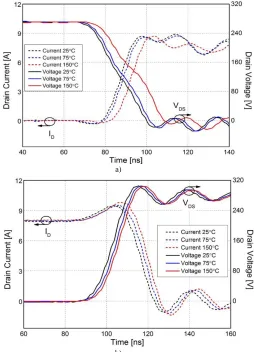
However, in the investigation of switching transients, as can be observed from Fig. 12, no pronounced temperature dependencies were observed for both dIDS/dt and dVGS/dt. The switching rate for both turn ON and turn OFF transients remain the same with the increasing of temperature. The only difference is the time delay on the switching of the device when the temperature increases. The estimated temperature sensitivity of turn ON delay is around 0.04 ns/oC and that of turn OFF delay is approximately 0.05 ns/oC. These temperature sensitivities are very low and it is difficult to achieve accurate temperature measurement. Therefore, based on the experiment results, the dIDS/dt is not a suitable TSEP for PGA26E19BA HEMT. Alternately, another TSEP IG is explored. Fig. 13 shows the temperature dependency of gate current with 1A saturation drain-source current and 9.7V gate-source bias voltage. In this way, the current drawn by the system is down to the device properties and the effect of self-heating is limited since the drain current is in relatively low level. 9.7V gate bias voltage was selected to achieve 3.5V on the gate of the device (a typical gate bias voltage in the datasheet of PGA26E19BA [11]). A linear variation with temperature was observed and IG increases with temperature. The corresponding temperature sensitivity is 2.458 mA/oC.
IV. COMPARISION OF DIFFERENT TSPES
Here comes to the stage where 5 TSEPs of SCT2080KE MOSFET and 6 TSEPs of PGA26E19BA HEMT have been explored. The temperature characteristics of these TSEPs are different in both quantitative and qualitative views. In order to select the a suitable TSPE under specific conditions, it is very interesting to investigate the advantages and disadvantages of these TSPEs [3,12]. Therefore, a comparison in terms of four criteria is discussed: temperature sensitivity, linearity, material and capability of on-line temperature monitoring. The TSEP dIDS/dt in PGA26E19BA HEMT is not included in the comparison of temperature sensitivity and linearity, since there is no noticeable temperature dependency observed in this TSPE based on the experiment result (Chapter III. B).
a) Temperature sensitivity: The temperature sensitivity of TSEPs is discussed in SiC and GaN in Table 1 & Table 2 separately. In SCT2080KE MOSFET, the gate threshold votlage could be considered as the most effcitive voltage monitor with relatively highest temperature sensitivity of 7.045 mV/oC, while the dI
DS/dt could be used as a good current monitor with temperature sensitivity of 1.367 (mA/ns) / oC (Table 1). Similarly, considering PGA26E19BA HEMT, the
gate threshold voltage can also be an effective TSEP with relatively good temperature sensitivity of 1.135 mV/oC and the gate current is a suitable current monitor with temperature sensitivity of 2.458 mA/oC. In particular, the temperature sensitivity of transconductance looks very promising with value of 6.330 mS/oC (Table 2).
a)
b)
Figure 12: Turn ON transient temperature dependency of PGA26E19BA HEMT: drain-source current vs Temperature & drain-source voltage vs
Temperature, a); Turn OFF transient temperature dependency of PGA26E19BA HEMT: drain-source current vs Temperature & drain-source
[image:4.612.335.589.123.475.2]voltage vs Temperature b).
Figure 13: Temperature dependency of gate current with 1A saturation drain current at 9.7V gate-source bias voltage of PGA26E19BA HEMT.
1.2 1.4 1.6 1.8 2 2.2
35 60 85 110 135 160
gm
(S
)
Temperature (oC)
6.15 6.2 6.25 6.3 6.35 6.4 6.45 6.5
15 65 115 165
IGS
(m
A
)
[image:4.612.334.587.544.697.2]Table 1: Comparison of TSEPs in SCT2080KE MOSFET
Table 2: Comparison of TSEPs in PGA26E19BA HEMT
Table 3: Comparison of TSEPs between SiC & GaN devices
b) Linearity: The linear temperature dependency of electrical parameters has a considerable effect on the simplification of the calibration process. In addition, it can also extend effective temperature sensing range and improve the accuracy of the temperature measurement. In the SCT2080KE MOSFET, the source-drain reverse bias voltage as well as the gate threshold voltage have almost perfect linear variation with temperature (Table 1). In the PGA26E19BA HEMT, it is found that both the gate threshold voltage and the gate current under biased drain current share excellent linearity with temperature (Table 2).
c) Material: The influence of different semiconductor material on the TSEPs is discussed in quantitative and qualitative effects separately (Table 3). Firstly, the source-drain reverse bias voltage, as the temperature increases, the value of VSD in SCT2080KE MOSFET reduces linearly whereas it almost remains unchanged in PGA26E19BA HEMT. Considering the static on-resistance, it is shown that the qualitative effect of temperature on the static on-resistance for both SiC and GaN transistors is in the same direction, where the values of static on-resistance increase linearly with temperature. However, the quantitative difference between these two devices is considerable. The temperature sensitivity
of PGA26E19BA HEMT is twice as large as that of SCT2080KE MOSFET with values of 1.064 mΩ/oC and 0.3873 mΩ/oC accordingly. For the gate threshold voltage, the temperature coefficients of VGS(TH) and gm for both SiC and GaN transistors are negative while the quantitative differences are significant. Although there is some contribution of larger drain current is chosen in SiC device, the temperature sensitivity of VGS(TH) is much higher in SCT2080KE MOSFET than that in GaN HEMT with values of 7.045 mV/oC and 1.135 mV/oC respectively. Whereas, the PGA26E19BA HEMT has much higher temperature sensitivity than SCT2080KE MOSFET in terms of transconductance (gm) with values of 6.330 mS/oC and 0.8 mS/oC correspondingly. In addition, noticeable difference is observed in dIDS/dt switching transient. The turn ON switching rate increases with temperature in SCT2080KE MOSFET due to the negative coefficient of gate threshold voltage. However, there is no obvious temperature dependency of dIDS/dt in PGA26E19BA HEMT.
d) Capability of on-line temperature monitoring: The real-time junction temperature could affect the performance, reliability and robustness of the system. In addition, it is also related to the device degradation and can be used as damage indicators. Therefore, it is important to develop some TSEPs TSPEs
Source-drain
reverse bias voltage Static on-resistance Gate threshold voltage Transconductance
dIDS/dt switching transient
Test condition
IS = 0.2A, VGS = 0V
ID = 0.1A,
VGS = 18V ID = 4.4mA
VDS = 0.75V, VGS from 15V to 19V
VIN = 400V, VGS = 18V, ID = 25A Temperature
sensitivity 3.765 mV / oC 0.3873 mΩ / oC 7.045 mV / oC 0.8 mS / oC 1.367 (mA/ns) / oC
Linearity VSD∝ 1/T RDS,ON∝ T VGS(TH) ∝ 1/T gm∝ 1/T dI/dt ∝ T
TSPEs
Source-drain
reverse bias voltage Static on-resistance Gate threshold voltage Transconductance Gate current
Test condition
IS = 1A, VGS = 0V
ID = 0.1A, IGS = 10mA
ID = 0.2mA VDS= 2V,
VDS = 1.5V, VGS from 2V to 3V
ID = 1A (saturated) VGS = 9.7V Temperature
sensitivity 0.141 mV / oC 1.064 mΩ / oC 1.135 mV / oC 6.330 mS / oC 2.458 mA/oC
Linearity
almost independent
(slightly increase) RDS,ON ∝ T VGS(TH) ∝ 1/T gm∝ 1/T IG ∝ T
TSPEs
Source-drain
reverse bias voltage Static on-resistance Gate threshold voltage Transconductance
SCT2080KE MOSFET
Sensitivity 3.765 mV / oC 0.3873 mΩ / oC 7.045 mV / oC 0.8 mS / oC
Linearity VSD∝ 1/T RDS,ON∝ T VGS(TH) ∝ 1/T gm∝ 1/T
PGA26E19BA HEMT
Sensitivity 0.141 mV / oC 1.064 mΩ / oC 1.135 mV / oC 6.330 mS / oC
that are able to measure the real-time temperature of power semiconductor devices. The dIDS/dt during the turn ON transient could be an effective TSPE to monitor the on-line temperature of SCT2080KE MOSFET. Alternatively, for the PGA26E19BA HEMT, the gate current under biased drain current could be considered.
V. CONCLUSION
Six TSEPs including source-drain reverse bias voltage (VSD), static on-resistance (RDS,ON), gate threshold voltage
(VGS(TH)), transconductance (gm), dIDS/dt switching transients
and gate current (IG) are investigated in terms of two kinds of semiconductor devices, SCT2080KE MOSFET & PGA26E19BA HEMT. These TSEPs are then compared based on four criteria: temperature sensitivity, linearity, material and the capability of on-line temperature monitoring. In SCT2080KE MOSFET, VSD , VGS(TH) and gm decreases with temperature linearly with calculated temperature sensitivity of 3.765 mV/oC, 7.045 mV/oC and 0.8 mS/oC correspondingly. By contrast, the RDS,ON is directly proportional to temperature with temperature sensitivity of 0.3873 mΩ/oC. In addition, it is found that the dIDS/dt during turn ON transient increases with temperature and the temperature sensitivity is 1.367 (mA/ns) / oC, which can be measured using magnetic flux sensor
combined with oscilloscope. The increasing of switching rate can be attributed to the negative coefficient of gate threshold voltage.
In comparison, for PGA26E19BA HEMT, there is no noticeable temperature dependency observed in VSD and dIDS/dt. The VSD almost remains constant with increasing of temperature. Switching time delay was observed when the temperature increases for both turn ON and turn OFF transients. However, the temperature sensitivities of these time delays are very low and thus it cannot achieve accurate temperature measurement. Alternatively, another TSEP IG is explored. IG shares a linear variation with temperature with sensitivity of 2.458 mA/oC. Similar results are presented in
RDS,ON, VGS(TH) and gm. RDS,ON increases with temperature and
the sensitivity is 1.064 mΩ/oC. Both V
GS(TH) and gm are
inversely proportional to temperature with sensitivities of 1.135 mV/oC and 6.330 mS/oC.
In terms of temperature sensitivity, the gate threshold voltage could be an effective TSEP for both SiC and GaN devices (7.045 mV/oC in SiC and 1.135 mV/oC in GaN). In particular, the temperature sensitivity of gm in GaN is much higher than that in SiC (6.330 mS/oC and 0.8 mS/oC correspondingly). Considering the linearity, the VSD and
VGS(TH) in SiC device share linear variation with temperature.
whereas, the RDS,ON and VGS(TH) increase linearly with temperature in GaN device. The dIDS/dt is capable to measure the on-line temperature of SiC device and the accuracy can be enhanced by mean of consecutive measurements. For the GaN device, the IG under biased drain current can be considered for real-time temperature monitoring.
VI. REFERENCES
[1] D. L. Blackburn, "Temperature measurements of semiconductor devices - a review," Twentieth Annual IEEE Semiconductor Thermal
Measurement and Management Symposium (IEEE Cat.
No.04CH37545), 2004, pp. 70-80. doi:
10.1109/STHERM.2004.1291304.
[2] J. O. Gonzalez, O. Alatise, J. Hu, L. Ran and P. A. Mawby, "An Investigation of Temperature-Sensitive Electrical Parameters for SiC Power MOSFETs," in IEEE Transactions on Power Electronics, vol. 32, no. 10, pp. 7954-7966, Oct. 2017. doi: 10.1109/TPEL.2016.2631447. [3] Y. Avenas, L. Dupont and Z. Khatir, "Temperature Measurement of
Power Semiconductor Devices by Thermo-Sensitive Electrical Parameters—A Review," in IEEE Transactions on Power Electronics, vol. 27, no. 6, pp. 3081-3092, June 2012. doi: 10.1109/TPEL.2011.2178433.
[4] Y. Cui, M. Chinthavali and L. M. Tolbert, "Temperature dependent Pspice model of silicon carbide power MOSFET," 2012 Twenty-Seventh Annual IEEE Applied Power Electronics Conference and Exposition
(APEC), Orlando, FL, 2012, pp. 1698-1704.
doi: 10.1109/APEC.2012.6166050.
[5] ROHM, 2012. SCT2080KE datasheet. [pdf] Available at: <http://www.rohm.com/web/global/datasheet/SCT2080KE/sct2080ke-e> [Accessed 01 January 2018].
[6] D. Barlini, M. Ciappa, M. Mermet-Guyennet, W. Fichtner, Measurement of the transient junction temperature in MOSFET devices under operating conditions, Microelectronics Reliability, Volume 47, Issues 9– 11, 2007, Pages 1707-1712, ISSN 0026-2714, https://doi.org/10.1016/j.microrel.2007.07.008.
[7] Baliga, B. (2008). Fundamentals of power semiconductor devices / B. Jayant Baliga. New York ; London.
[8] Perret, R. (2009). Power electronics semiconductor devices / edited by Robert Perret. London : Hoboken, N.J.
[9] Y. Uemoto et al., "Gate Injection Transistor (GIT)—A Normally-Off AlGaN/GaN Power Transistor Using Conductivity Modulation," in IEEE Transactions on Electron Devices, vol. 54, no. 12, pp. 3393-3399, Dec. 2007. doi: 10.1109/TED.2007.908601.
[10] Tetsu Kachi, Current status of GaN power devices, IEICE Electronics Express, Released November 10, 2013, Online ISSN 1349-2543, ttps://doi.org/10.1587/elex.10.20132005.
[11] Panasonic, 2015. PGA26E19BA preliminary datasheet. [pdf] Available at:<http://www.mouser.com/ds/2/315/PreliminarySMDGANDatasheet PGA26E19BA-1093291.pdf> [Accessed 03 January 2018].