Optimisation of pH of the CdCl2+Ga2(SO4)3 activation step
of CdS/CdTe based thin-film solar cells
OJO, A.A. and DHARMADASA, I <http://orcid.org/0000-0001-7988-669X>
Available from Sheffield Hallam University Research Archive (SHURA) at:
http://shura.shu.ac.uk/21411/
This document is the author deposited version. You are advised to consult the publisher's version if you wish to cite from it.
Published version
OJO, A.A. and DHARMADASA, I (2018). Optimisation of pH of the
CdCl2+Ga2(SO4)3 activation step of CdS/CdTe based thin-film solar cells. Solar Energy, 170, 398-405.
Copyright and re-use policy
See http://shura.shu.ac.uk/information.html
1
Optimisation of pH of the CdCl2+Ga2(SO4)3 Activation Step of CdS/CdTe Based
Thin-Film Solar Cells
A.A. Ojo* and I.M. Dharmadasa
Electronic Materials and Sensors Group, Materials and Engineering Research Institute (MERI), Sheffield Hallam University, Sheffield S1 1WB, UK.
*Email: [email protected]; Tel: +44 114 225 6910 Fax: +44 114 225 6930
Abstract
In order to produce high efficiency solar cells based on CdTe, CdCl2 post-growth treatment is
an essential processing step. This treatment can be further improved by adding elements such
as Fluorine and Gallium into the CdCl2 solution. Through systematic experimentation, it has
been found that the pH value of the treatment solution also affect the conversion efficiency of
the solar cells. This work therefore focuses on the effect of pH value of CdCl2+Ga2(SO4)3
aqueous solution on the device efficiencies. The graded bandgap device structure,
glass/FTO/n-ZnS/n-CdS/n-CdTe/Au was used in this work. The pH values of 1.00, 2.00 and
3.00 for CdCl2+Ga2(SO4)3 solutions were utilised for the activation of glass/FTO/n-ZnS/n
-CdS/n-CdTe layers and its effects were explored for both the CdTe material and device
properties. It has been found that both CdTe material properties and solar cell device
properties are superior when the pH value of 2.00 is used for post-growth treatment. The best
conversion efficiency observed in this work for the above graded bandgap device is 12.2%.
2
1 Introduction
Tellurium (Te) precipitation in cadmium telluride (CdTe) has been a known issue in CdTe
layers irrespective of the growth technique (Fernández, 2003). An integral part of achieving a
reduction in Te precipitation and highly efficient solar cells has been dependent on the
post-growth treatment (PGT) of CdTe in the presence of excess Cd, chlorine (Dharmadasa, 2014)
and fluorine (Rios-Flores et al., 2012) (CdCl2 treatment). Amongst the advantages associated
with PGT includes the improvement in grain growth, recrystallisation, optical property,
electrical conductivity, doping concentration, grain boundary passivation, improved Cd/Te
composition, CdS/CdTe interface morphology (Basol, 1992; Bosio et al., 2006; Dharmadasa
et al., 2017; Liu et al., 2015; Xue et al., 2016) and reduction in native defects (I. M.
Dharmadasa et al., 2015). Different post-growth treatments have been utilised for the
improvement of the characteristic properties of CdTe as documented in the literature (Major
et al., 2016, 2015; Mis-Fernández et al., 2017; Williams et al., 2015). Based on the ability of
gallium to dissolve Te-precipitates in CdTe (Fernández, 2003; Sochinskii et al., 1993), our
previous research work has been focused on its incorporation in the usual CdCl2 treatment of
CdTe (Ojo et al., 2017; Olusola et al., 2017) from which high-efficiency CdS/CdTe-based
devices were fabricated with improved material and electronic properties. So far, the effect of
pH on the CdCl2+Ga2(SO4)3 (GCT) post-growth treatment of CdS/CdTe based solar cell is
yet unknown. In the present study, the focus was on the effect of pH on the CdCl2+Ga2(SO4)3
PGT with the aim to further improve both the material and electronic properties of
glass/FTO/n-ZnS/n-CdS/n-CdTe/Au devices fabricated.
2 Experimental details
All the chemicals and glass/FTO substrates utilised in this sets of experiments were bought
from Sigma Aldrich UK. Two-electrode electroplating technique was employed for all the
deposited semiconductors utilised in this work in which a high purity graphite electrode is the
anode, and transparent conducting oxide (TCO) was used as the cathode. The specification of
the glass/fluorine-doped tin oxide (FTO) utilised in this work is TEC-7 with a sheet resistance
of ~7 Ω/□. Prior to the electroplating, the glass/FTO substrates were cut into 4×3 cm2,
ultrasonically washed for 15 min in soap water, rinsed in deionised (DI) water, degreased
using acetone and rinsed afterwards in a flow of DI water. Before the transfer of the
glass/FTO into the electrolytic bath, the substrate is attached to a high purity graphite rod
using polytetrafluoroethylene (PTFE) tape but only the FTO surface was in contact with the
3
2.1 Sample preparation
The n-ZnS buffer layer was electrodeposited (ED) on the glass/FTO substrates from an
electrolyte containing zinc sulphate monohydrate (ZnSO4⸱H2O) and ammonium thiosulphate
((NH4)2S2O3) with respective purity of 99.9% and 98%. The electrolytic bath was prepared
by mixing 0.2 M ZnSO4⸱H2O and 0.2 M (NH4)2S2O3 aqueous solutions in 400 ml plastic
vessel to use as zinc and sulphur precursors respectively. For this work, 50 nm thick n-ZnS
layers were electroplated at a cathodic voltage of 1425 mV close to the p-to-n conduction
type transition voltage (Vi). Details of the ED-ZnS has been documented in the literature
(Madugu et al., 2016). The electrodeposited glass/FTO/n-ZnS layers were annealed in air at
300℃ and air-cooled afterwards. It should be noted that the conduction type of the n-ZnS is
retained after annealing (Madugu et al., 2016).
65 nm thick n-CdS window layers were electroplated on the post-growth treated glass/FTO/
n-ZnS layers. The CdS was electroplated from an aqueous electrolyte containing 0.3 M
hydrated cadmium chloride (CdCl2⸱xH2O) and 0.03 M ammonium thiosulphate ((NH4)2S2O3)
with respective purity of 99.99% and 98% in 400 ml of DI water. The CdS layers were
deposited at a pre-optimised cathodic voltage of 1200 mV (Abdul-Manaf et al., 2015). The
deposited glass/FTO/n-ZnS/n-CdS structure was annealed in the presence of CdCl2. The
CdCl2 treatment was performed by adding few drops of aqueous solution containing 0.1 M
CdCl2 in 20 ml of DI water to the surface of the semiconductor layer. The full coverage of the
layers with the treatment solutions was achieved by spreading the solution using
solution-damped cotton bud. The semiconductor layer was allowed to air-dry and heat treated at
400℃ for 20 min. The treated glass/FTO/n-ZnS/n-CdS layers were air-cooled and rinsed in
DI water before n-CdTe layer deposition. Full details of deposition and optimisation of
ED-CdS layer has been published in the literature (Abdul-Manaf et al., 2015). It should be noted
that CdS layers are intrinsically n-type due defects related to Cd interstitials and S vacancies
in CdS layers (Sathaye and Sinha, 1976).
1150 nm thick n-CdTe layers were electrodeposited at 1400 mV on the glass/FTO/n-ZnS/
n-CdS substrate. The CdTe layers were deposited from an electrolyte containing 1.5 M
cadmium nitrate tetrahydrate (Cd(NO3)2⸱4H2O) and 0.0023 M tellurium dioxide (TeO2) with
respective purity of 99.0% and 99.99% in 400 ml of deionised water. Full details of
deposition, characterisation and optimisation of the electroplated CdTe layers has been
documented in the literature (Salim et al., 2015). Prior to GCT activation process of the
glass/FTO/n-ZnS/n-CdS/n-CdTe, the 4×3 cm2 glass/FTO/n-ZnS/n-CdS/n-CdTe layers were
4
The CdCl2+Ga2(SO4)3 solution utilised for the GCT was prepared in aqueous solution
containing 0.1 M CdCl2 and 0.05 M Ga2(SO4)3 in a 60 ml of DI water. The solution was
stirred for 60 min to achieve homogeneity and 20 ml of the solution was poured into three
different 25 ml glass beakers. The pH of the CdCl2+Ga2(SO4)3 solutions were adjusted to
1.00±0.02, 2.00±0.02 and 3.00±0.02 using dilute HCl solution. Afterwards, the glass/FTO/
n-ZnS/n-CdS/n-CdTe layers were treated using CdCl2+Ga2(SO4)3 solutions of different pH,
dried in air and heat treated at 400℃ for 20 min in air atmosphere (Ojo et al., 2017). The full
coverage of the layers was achieved by the use of solution damped cotton buds.
The annealed glass/FTO/n-ZnS/n-CdS/n-CdTe layers were etched using aqueous solutions
containing H2SO4 and K2Cr2O7 for acid etching, and NaOH and Na2S2O3 for alkaline etching
for 2 s and 2 min respectively to improve the metal/semiconductor contact (Dharmadasa et
al., 1998). The glass/FTO/n-ZnS/n-CdS/n-CdTe layers were immediately transferred to a
high vacuum system to deposit 100 nm thick Au contacts of 2 mm diameter on the
glass/FTO/n-ZnS/n-CdS/n-CdTe structure at a low pressure of 10-5 Nm-2.
2.2 Graded bandgap configuration
The basic concept behind graded bandgap (GBG) solar cell is the possibility of effective
harnessing of photons across the ultraviolet (UV), visible (Vis) and infrared (IR) regions
(Dharmadasa, 2005). This concept has been validated in the literature across organic (Ergen
et al., 2016), inorganic (Dharmadasa et al., 2011; I.M. Dharmadasa et al., 2015) and hybrid
(Dharmadasa, 2005; Ergen et al., 2016) solar cell technology. Graded bandgap can be
achieved by grading the semiconductor layers in such a way that the bandgap varies
throughout the entire thickness (Dharmadasa et al., 2011). GBG can also be produced by
successively growing semiconductor materials on top of each other in which the layers are
arranged such that the bandgap decreases gradually while the conductivity type gradually
changes from one type to the other (Dharmadasa, 2005).
The earliest work that theoretically described the functionality of GBG configuration was
reported by Tauc in 1957 (Tauc, 1957). His work elucidates the possibility of GBG solar cell
configuration attaining higher conversion efficiency above the well-explored p-n junction
cells stimulated interest in the photovoltaic research community. Taking into consideration
the photogenerated current, it was proven theoretically that GBG solar cell configurations are
capable of attaining a conversion efficiency of ~38% under AM1.5 (Emtage, 1962; Wolf,
1960) as compared to the 23% of single p-n junction solar cells. Based on this theoretical
5
1970s (Hovel and Woodall, 1973; Konagai and Takahashi, 1975) by gradual doping of only
p-type gallium arsenide (GaAs) with aluminium. The published work demonstrated a
single-sided p-type grading of p-Ga1-xAlxAs/n-GaAs solar cell. In 2002, the first model of full solar
cell device bandgap grading was proposed and published by Dharmadasa et al (Dharmadasa
et al., 2002). The full graded bandgap (GBG) architectures as proposed in the literature
(Dharmadasa et al., 2005; Dharmadasa, 2005) can be accomplished by the incorporation of
either an n-type or p-type wide bandgap front-layer with a steady reduction in bandgap
towards p-type or n-type back layer respectively.
The glass/FTO/n-ZnS/n-CdS/n-CdTe/Au graded bandgap configuration examined in this
work (see Figure 1) is relative to the technology as documented in the literature (Dharmadasa
et al., 2005). It should be noted that the incorporated semiconductor layers (ZnS, CdS, and
CdTe) have been individually examined and documented in the literature (Abdul-Manaf et
al., 2015; Madugu et al., 2016; Salim et al., 2015). Asides from the bandgap grading of ZnS
(3.72 eV (Madugu et al., 2016)), CdS (2.42 eV (Abdul-Manaf et al., 2015)), and CdTe (1.50
eV (Salim et al., 2015)), there are possible formation of ZnxCd1-xS and CdSxTe1-x ternary
compounds in-between successively deposited semiconductor layers due to interface
interaction and chemical reactions. Literature on bandgap grading based on incorporated
ZnS/CdS/CdTe layers have been well established in the literature (Han et al., 2013; Oladeji
and Chow, 2005).
Figure 1: A typical band diagram of graded bandgap glass/FTO/n-ZnS/n-CdS/n-CdTe/Au
[image:6.595.184.442.474.670.2]6
As documented in the literature, the formation of such ternary compound is attributable to the
interdiffusion of elemental Zn & Cd across the ZnS/CdS interface (Oladeji and Chow, 2005)
and S & Te (Li et al., 2014) across the CdS/CdTe interface during the post-growth treatment
processes. The formed ternary compounds also participate in the bandgap grading due to
continuous band bending as observed in Figure 1. Further to this, the n-CdTe/metal interface
(Dharmadasa et al., 1998) creates a large Schottky barrier (SB), which provides the main
electric field in the glass/FTO/n-ZnS/n-CdS/n-CdTe/Au GBG configuration. As shown in
Figure 1, the effective separation of the photogenerated e-h pairs is achievable as depicted by
the propagation of the depletion region across all the layers.
2.3 Characterisation techniques
The work reported in this manuscript is focused on device properties, but the mentioned
material properties such as the analyses of both the morphology and composition of the
deposited layers were studied using FEI Nova 200 NanoSEM equipment with an
Energy-dispersive X-ray spectroscopy (EDX) compartment. The optical properties of the grown thin
films were investigated at room temperature using Cary 50 Scan Ultraviolet-Visible
(UV-Vis) spectrophotometer within the wavelength range of (200 – 1000) nm. X-ray diffraction
(XRD) was utilised for acquiring information about the level of crystallinity, identification of
elements, compounds and phases of the deposited layers. The XRD equipment utilised was
Philips PW 3710 X’pert diffractometer with Cu-Kα monochromator of wavelength λ=1.54 Å.
The X-ray generator tension and generator current were respectively set to 40 kV and 40 mA.
The conduction types were determined using Photoelectrochemical (PEC) cell measurement.
The layers utilised for the PEC measurement was 2×3 cm2 glass/FTO/n-CdTe layer with a
CdTe thickness of 1150 nm grown at 1400 mV. The DC conductivity measurements were
carried out on glass/FTO/CdTe/ohmic contact structures using Rera Solution fully automated
I-V system. Depending on the conduction type of the CdTe in the glass/FTO/CdTe layer after
post-growth treatment, 100 nm thick Au was deposited on p-CdTe or Al on n-CdTe to
achieve Ohmic contacts prior to DC conductivity measurements.
The main device characterisation techniques utilised for the analysis of the fabricated
glass/FTO/n-ZnS/n-CdS/n-CdTe/Au devices were the current-voltage (I-V) and
capacitance-voltage (C-V) methods. The I-V characterisations were performed under both dark and
AM1.5 illuminated conditions using fully automated Rera Solution PV simulation system.
The Rera Solution PV measurement system is comprised of a Keithley 2401 SourceMeter,
7
software. The system was calibrated before use, using RR267MON standard reference
Si-based cell prior to measurements. The C-V measurements were carried out using fully
automated HP 4284A Precision LCR meter at a detecting signal frequency of 1 MHz under
dark condition. For both the I-V and C-V measurements, the bias range was set between −1.0
V and +1.0 V at 300 K for all the measurements taken.
3 The effects of pH value of the CdCl2+Ga2(SO4)3 treatment solution on properties of
CdTe layer
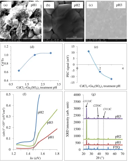
Figure 2(a-c) show the respective morphology of the glass/FTO/n-ZnS/n-CdS/n-CdTe layers
activated with GCT solution at pH1, pH2 and pH3. Figure 2(d) and Figure 2(e) show the
compositional analysis and the photoelectrochemical (PEC) cell measurement results of the
glass/FTO/CdTe activated with GCT solution at pH1, pH2, and pH3. Figure 2(f) and Figure
2(g) show the Tauc’s plot, and the XRD diffraction of the glass/FTO/CdTe layers activated
with GCT solution at pH1, pH2 and pH3. Further to the material summary captured in Figure
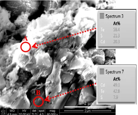
2, Figure 3 shows the point compositional EDX analysis on the glass/FTO/CdTe layer treated
with pH1 GCT.
With respect to Figure 2(a-c), the morphology of the layers show the presence of large grains
with sizes >2 µm as observed for samples treated with GCT of pH2, while samples treated
with GCT of pH3 and pH1 show smaller grains size averaging ~1 µm. Consequently, the best
underlying glass/FTO substrate coverage was observed for the glass/FTO/n-ZnS/n-CdS/
n-CdTe layers treated with GCT pH3 followed by the pH2 and the pH1 treated layers. But the
pH1 GCT treated layers show a striking erosion of surface, due to the harshness of the acidic
concentration of the treatment solution. The presence of Te-rich strands was also observable
due to the dissolution of elemental Cd from the CdTe layers as depicted in Figure 2(a) and
Figure 3. It is well known that an introduction of an acidic media to CdTe attacks Cd
preferentially leaving Te rich surface (Dharmadasa, 1998). In the case of the pH1 GCT
treated layer, the layers were eroded leaving behind Te-rich surface and high pinhole density.
The presence of high pinhole density of the pH1 GCT glass/FTO/n-ZnS/n-CdS/n-CdTe
signifies the detrimental effect of the high acidity (low pH) of the treatment solution. It
should also be taking into consideration that the grain growth observed after post-growth
treatment of CdTe under favourable conditions are mainly attributed to the recrystallization,
coalescence and Ostwald ripening of grains amongst other factors (Dharmadasa, 2014;
McCandless and Sites, 2011). But due to the thinness of the films (within nano-scale), the
8
electroplated materials, the erosion of the CdTe surface will result in opening pores along the
grain boundaries which may lead into shunt paths for charge carriers as in the case of pH1
[image:9.595.74.513.156.709.2]GCT treated layer (see Figure 2(a)).
Figure 2: Typical results of SEM, EDX, PEC, optical absorption and XRD measurements
for CdTe post-growth treated with pH1, pH2 and pH3 CdCl2+Ga2(SO4)3 solutions.
0 0.1 0.2 0.3 0.4 0.5
1.2 1.4 1.6 1.8
(
αhv
)
2 ×
10
11 (
eV
2cm 2)
hv (eV)
pH1 pH2 (f) pH3 -15 -10 -5 0 5 10 15
0 2 4
PE C si g nal ( m V )
CdCl2+Ga2(SO4)3 treatment pH (e) 0 500 1000 1500 2000 2500 3000 3500 4000
20 30 40 50 60 70
XRD int ensit y (a rb. unit ) 2θ (°) pH1 pH2 FTO (g) pH3 (111)C (220)C (311)C pH1
(a) (b) pH2 (c) pH3
0.4 0.6 0.8 1.0 1.2
0.5 1.5 2.5 3.5
C
d/
Te
9
As regards the compositional analysis as shown in Figure 2(d), the observable trend of the
Cd/Te ratio for the glass/FTO/n-ZnS/n-CdS/n-CdTe layers treated with GCT of pH3, pH2
and pH1 shows a >1.0, ~1.0 and <1.0 respectively. This observation can be attributed to the
effect of increased acidity and acid etching resulting in the preferential dissolution of Cd from
the CdTe surface (Dharmadasa, 2014; Williams et al., 2014). The alteration of the Cd to Te
ratio from >1.0, tending towards ~1.0 and <1.0 for the glass/FTO/n-ZnS/n-CdS/n-CdTe
layers treated with GCT of pH3, pH2 and pH1 are documented in the literature as one of the
factors determining the conduction type of CdTe layers (Dharmadasa, 2014; Williams et al.,
2014).
The photoelectrochemical cell measurement as shown in Figure 2(e) depicts a gradual
transition of conduction type from p-type CdTe treated with pH1 GCT, to n-type CdTe
treated with pH2 GCT (but close to p-type) and to an n-type conduction type for the
glass/FTO/CdTe layers treated with pH3 GCT. It was therefore interesting to observe that the
PEC cell measurements as shown in Figure 2(e) is in accord with the summations of the
compositional analysis. The Te-rich CdTe surfaces show p-type electrical conduction and
Cd-rich CdTe surfaces show n-type electrical conduction. It should be noted that the
determination of conduction type and the possible transition of one conduction type to
another after heat treatment of CdTe is not just determined by the composition of Cd/Te.
Other factors documented in the literature include the doping effect caused by pre-annealing
treatment, annealing duration and temperature, the initial atomic composition of Cd/Te, the
A
B
Figure 3: SEM micrograph of glass/FTO/n-ZnS/n-CdS/n-CdTe layers treated with GCT at
pH1 and the EDX point micrographs on different parts of the CdTe layer; at points A
[image:10.595.179.416.83.280.2]10
structure of the defect in the initial CdTe layer and the initial conductivity type of the material
(Basol, 1992; Dharmadasa, 2014; Salim et al., 2015).
Pertaining to Figure 2(f), the absorbance for the glass/FTO/n-ZnS/n-CdS/n-CdTe layers
activated with GCT of pH1, pH2 and pH3 was observed from Tauc’s plot of (αhv)2 against hv
where α is the absorption coefficient, h is the plank’s constant and v is the incident photon
frequency and λ is the wavelength (Tauc, 1968). Based on observation, all the glass/FTO/n
-ZnS/n-CdS/n-CdTe layers with treated GCT pH1, pH2 and pH3 all show a bandgap of
~1.47±0.01 eV. The observed bandgaps are comparative to the bandgap of bulk CdTe. More
importantly, the sharpness of the absorption edge slope for all the glass/FTO/n-ZnS/n-CdS/n
-CdTe layers differs (see Figure 2(f)). As documented in the literature, the steeper the
absorption edge the more the superiority of the semiconductor layer is based on lesser
impurity energy levels and defects in the thin film (Bosio et al., 2006). Based on this
submission, it could be interpreted that the glass/FTO/n-ZnS/n-CdS/n-CdTe layers activated
with pH2 GCT are superior to others.
The structural analysis performed using XRD is depicted in Figure 2(g) with the plot of XRD
diffraction intensity against 2θ°. The XRD patterns shown in Figure 2(g) were stacked for
better comparison. The presence of (111), (220) and (311) cubic CdTe at 2θ=~23.8°,
2θ=~38.6° and 2θ=~45.8° were observed in all the XRD diffractions for all the glass/FTO/n
-ZnS/n-CdS/n-CdTe layers activated with pH1, pH2 and pH3 GCT. It should be noted that the
XRD diffraction patterns, other elements or compound overlapping with the CdTe and FTO
diffractions might be present. Based on the XRD diffraction peak intensity, the (111)C
orientation is considered as the preferred orientation of the CdTe layers and the summary of
the structural data is captured in Table 1. The extracted XRD data from these CdTe work
matches the JCPDS reference file number 01-075-2086-cubic. It should be noted that
Scherrer’s formula (see equation (1)) was utilised for the calculation of the crystallite size D,
where θ is the Bragg angle, β is the full width at half maximum (FWHM) of the diffraction
peak in radian and λ is the wavelength of the X-rays used (1.54 Ǻ).
cos 94 . 0
D (1)
As observations in Figure 2(g) and Table 1, the highest and the least peak intensity was
observed for the glass/FTO/n-ZnS/n-CdS/n-CdTe layers activated with pH2 and pH1 GCT
respectively. The comparatively low (111)C diffraction intensity observed for the layers
activated with pH3 and pH1 GCT might be due to the richness of Cd and Te in the CdTe
11
crystallinity of 65.4 nm was observed for the layers activated with pH2 GCT. It should be
noted that the crystallite size as calculated using XRD does not correspond to the grain size as
seen on the SEM micrograph but the grains are formed from several crystallites.
4 The effects of pH value of the CdCl2+Ga2(SO4)3 treatment solution on properties of
solar cells
It should be noted that the melting point of CdTe is 1093°C. Therefore, during CdCl2
treatment, large columnar grown crystals of CdTe remain as solids (Amarasinghe et al., 2018;
Donghwan Kim et al., 1994; Harvey et al., 2015; Moutinho et al., 1998). However, the
presence of the impurities such as excess Cd, excess Te, Cl, O and Ga accumulate in grain
boundaries as a result of multi-element segregation after annealing process (Emziane et al.,
2005; Harvey et al., 2015; Mao et al., 2014; Mazzamuto et al., 2008; Tuteja et al., 2016), and
the melting point of grain boundary material reduces drastically to ~385±5°C (Dharmadasa et
al., 2014). Above this temperature, solid CdTe crystals float in a liquid of grain boundary
materials, grains grow by Oswald ripening, dope the surface of CdTe crystals using Cl and
Ga, and freeze improving the material in grain boundaries after cooling. This process
improves the main rectifying contact parallel to the TCO, and produce transverse p-n
junctions across the CdTe cylindrical surfaces. This additional p-n junctions help to separate
photo-generated e-h pairs instantly to travel in two different paths. One carrier travels through
the CdTe crystal and the other carrier travel through the grain boundary normal to the TCO
layer minimising recombination. This is known as grain boundary enhanced PV effect and
the full description can be found in a previous publication (Dharmadasa, 2014; Dharmadasa
et al., 2014; Dharmadasa and Ojo, 2017).
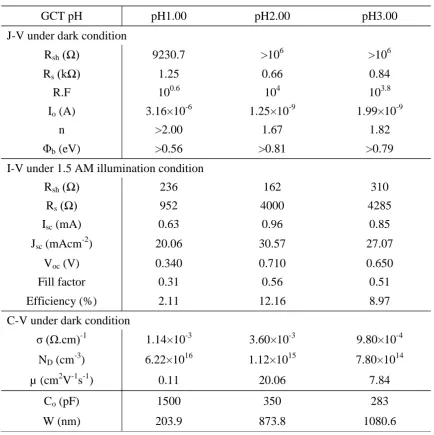
Figure 4 (a) depicts the J-V curves recorded for the glass/FTO/n-ZnS/n-CdS/n-CdTe/Au
devices fabricated from the pH1, pH2 and pH3 GCT layers measured under AM1.5
condition. Figure 4 (b) and Figure 4 (c) show the graph of capacitance against bias voltage
and the corresponding Mott–Schottky plot for the devices fabricated from the pH1 GCT
[image:12.595.75.504.173.243.2]glass/FTO/n-ZnS/n-CdS/n-CdTe/Au devices. Figure 4 (d) and Figure 4 (e) show the graph of Table 1: Summary of the X-ray diffraction analysis for cubic (111) CdTe diffraction.
Acidity 2θ (°)
Peak intensity (arb. unit)
d-spacing (Å)
FWHM (°)
Crystallite size (nm)
pH3 23.97 809 3.709 0.162 52.3
pH2 23.91 1451 3.718 0.129 65.4
12
capacitance against bias voltage and the corresponding Mott–Schottky plot for the device
fabricated from the pH2 GCT glass/FTO/n-ZnS/n-CdS/n-CdTe/Au devices. The measured
device summary is captured in Table 2. The effective Richardson constant (A*) utilised for
calculations has been predetermined as 12 Am-2K-2 for CdTe using Eq (2).
3 2 * * 4 h q k m
A
(2)Figure 4: (a) Typical current–voltage curves of the glass/FTO/n-ZnS/n-CdS/n-CdTe/Au
devices treated with pH1, pH2 and pH3 GCT, (b) Capacitance-voltage plot and (c)
Schottky-Mott plot under dark conditions for the cell fabricated from the pH1 GCT layers, (d)
Capacitance-voltage plot and (d) Schottky–Mott plot under dark conditions for the cells
fabricated from the pH2 GCT layers. 0.0
2.0 4.0 6.0
-1.0 -0.5 0.0 0.5 1.0
C × 10 -10 ( F) Bias (V) (d) 0.0 2.0 4.0 6.0 8.0
-1.0 -0.5 0.0 0.5 1.0
C
-2
×
10
18 (F -2) Bias (V) (e) 0.0 0.5 1.0 1.5 2.0 2.5
-1.0 -0.5 0.0 0.5 1.0
C
×
10
-9 (
F) Bias (V) (b) 0.0 1.0 2.0 3.0 4.0 5.0
-1.0 -0.5 0.0 0.5 1.0
C
-2 ×
10
17 (F -2) Bias (V) (c) -35 -25 -15 -5 5
-0.2 0 0.2 0.4 0.6 0.8
13
As depicted in the J-V section of Table 2, shunt resistance (Rsh) >1 MΩ were recorded for the
glass/FTO/n-ZnS/n-CdS/n-CdTe/Au devices activated with pH2 and pH3 as compared to the
low Rsh value of the pH1 GCT treated case. It should be noted that low Rsh values of
fabricated photovoltaic devices can be attributed to low semiconductor material quality to the
presence of pinholes, gaps, voids, and high dislocation density within the semiconductor
material (Soga, 2006) amongst others. It is not surprising that low Rsh value for the devices
fabricated from the pH1 glass/FTO/n-ZnS/n-CdS/n-CdTe GCT layers was observed due to
the eroded morphology and the optical summation as discussed in Section 3. Further to this,
rectification factor (RF) values higher than 3 orders of magnitude was observed for the
glass/FTO/n-ZnS/n-CdS/n-CdTe/Au activated with pH2 and pH3 GCT. As documented in
the literature, RF values equal or higher than 2.5 orders of magnitude is a characteristic
property of high-efficiency solar cells (Dharmadasa, 2013). The severe reduction in the RF
value for the devices fabricated from the pH1 GCT treated glass/FTO/n-ZnS/n-CdS/n-CdTe
can be ascribed to the CdTe material deterioration due to the harshness of the acidic
dissolution of Cd from the CdTe surface and the resulting surface erosion of the CdTe surface
as discussed in Section 3.
Likewise, the ideality factor (n) of the devices fabricated from the pH2 and pH3 GCT treated
glass/FTO/n-ZnS/n-CdS/n-CdTe lies between 1.00 and 2.00, while the n values for the pH1
treated layers were >2.00. This signifies that the dominating current transport mechanism of
the devices fabricated from the glass/FTO/n-ZnS/n-CdS/n-CdTe activated with pH2 and pH3
GCT is by both thermionic emission and recombination & generation (R&G) processes in
parallel. While the n value >2.00, observed for the devices fabricated from the pH1 GCT
layers signifies that the current transportation mechanism is dominated by R&G and the
tunnelling of high energy electron through the barrier height (Verschraegen et al., 2005),
which consequentially results in the reduction of the barrier height ɸb as depicted in Table 2.
With reference to Figure 4 (a) and the (AM1.5 illuminated condition) J-V section of Table 2,
short circuit current density (Jsc) higher than the Shockley-Queisser limit for single p-n
junction (Shockley and Queisser, 1961) was observed for the glass/FTO/n-ZnS/n-CdS/n
-CdTe/Au devices fabricated from the pH2 and pH3 GCT treated layers. The high Jsc can be
attributed to the multi-junction graded bandgap n-n-n+SB device configuration (Vos, 2000).
To ascertain the authenticity of the parameters measured, the cells under test were isolated by
carefully removing surrounding layers to avoid possible peripheral current collection as
suggested in the literature (Godfrey and Green, 1977). The collection of current from the
14
this work (Basol, 1984). Further to this, comparatively higher open-circuit voltage (Voc),
fill-factor (FF) and efficiency (η) were observed for the devices fabricated from the pH2 and pH3
GCT (but championed by pH2 GCT) as compared to the fabricated device using pH1 GCT
treated layer.
The C-V measurements presented in Figure 4 (b-e) and Table 2 were performed under dark
condition at a frequency of 1.0 MHz AC signal, bias range of (-1.00 to 1.00) V at 300 K. The
doping density (ND) and built-in potential (Vbi) for this devices were determined using the
Table 2: Summary of device and material parameters obtained from I-V (both under
illuminated and dark conditions) and C-V (dark condition) for glass/FTO/n-ZnS/n-CdS/n
-CdTe/Au solar cells activated with pH1, pH2 and pH3 GCT treatment.
GCT pH pH1.00 pH2.00 pH3.00
J-V under dark condition
Rsh (Ω) 9230.7 >106 >106
Rs (kΩ) 1.25 0.66 0.84
R.F 100.6 104 103.8
Io (A) 3.16×10⁻⁶ 1.25×10⁻⁹ 1.99×10⁻⁹
n >2.00 1.67 1.82
Φb (eV) >0.56 >0.81 >0.79
I-V under 1.5 AM illumination condition
Rsh (Ω) 236 162 310
Rs (Ω) 952 4000 4285
Isc (mA) 0.63 0.96 0.85
Jsc (mAcm-2) 20.06 30.57 27.07
Voc (V) 0.340 0.710 0.650
Fill factor 0.31 0.56 0.51
Efficiency (%) 2.11 12.16 8.97
C-V under dark condition σ (Ω.cm)-1
1.14×10⁻³ 3.60×10⁻³ 9.80×10⁻⁴
ND (cm-3) 6.22×10¹⁶ 1.12×10¹⁵ 7.80×10¹⁴
µ (cm2V-1s-1) 0.11 20.06 7.84
Co (pF) 1500 350 283
[image:15.595.80.515.234.670.2]15
Mott-Schottky plot as shown in Figure 4 (c) and Figure 4 (e) for the devices incorporated
layers activated with pH1 and pH2 GCT respectively. Equations (3) to (5) were also utilised.
R bi
D s V V N eA
C2 2
2 1 (3) 2 2 A eN Slope D s (4) slope eA N r
D 2
0 2
(5)
where C is the capacitance, ɛr is the relative dielectric constant, ɛo is the permittivity of free
space, ɛs is the semiconductor permittivity, e is the electronic charge, A is the area of the
contact, ND is the donor concentration, Vbi is the built-in potential and VR is the reverse bias
voltage. The slope and the intercept of the C-2 versus V plot are given by equation (3). The ɛr
value utilised for calculation was 11.0 (Strzalkowski et al., 1976), while the calculated
effective density of states of the conduction band (Nc) using equation (6) was 9.16×1017 cm-3,
where, h is the plank’s constant, T is the temperature, k is the Boltzmann’s constant and me* is
the effective electron mass.
2 3 2 2 2 h kT m N e C (6)
With the assumption that all donor atoms are ionised at 300 K (therefore n≈ND), the carrier
mobility µ⊥ was evaluated using equation (7), where σ is the electrical conductivity. Other
calculated parameters are shown in Table 2.
e N
ne D
(7)
As depicted in Table 2, the doping concentration of the devices fabricated from both the pH2
and pH3 GCT treated glass/FTO/n-ZnS/n-CdS/n-CdTe layers lies within the region
corresponding to the high-efficiency CdTe devices ~(1.0×10¹⁴ – 5×10¹⁵) cm-3 reported in the
literature (Britt and Ferekides, 1993; Woodcock et al., 1991). An increase in the doping
concentration of the fabricated devices from the pH1 GCT treated glass/FTO/n-ZnS/n-CdS/n
-CdTe layers to ~1016 cm-3 was observed. The high doping concentration recorded for the
activated layers using pH1 GCT results in the reduction in the depletion width, loss of
short-circuit current density and increment in defect density and the reduction in the
photo-generated current (Coutts and Naseem, 1985). As observed from the C-V section of Table 1
16
shows a deviation from the linearity as a result of the effects of defects, traps, surface states,
interfacial resistive layers (attributable to oxidation) producing excess capacitance and
inhomogeneity (Chaure et al., 2003). For the devices fabricated from the pH2 GCT treated
glass/FTO/n-ZnS/n-CdS/n-CdTe layers, full depletion at reverse biased and close to zero
biased voltages were observed. As shown in Figure 4 (e), an increase in the voltage towards
forward bias ~0.6 V, the depletion width W equals the device thickness of ~1300 nm. Above
~0.6 V, an increase in capacitance results was observed with increasing forward bias voltage
resulting into a gradual reduction in the depletion width. This observation is in accordance
with the Mott–Schottky theory and can be utilised for the estimation of the diffusion voltage
of the device (Vbi) and the excess donor concentration (ND-NA) for n-CdTe layer. Increase in
the mobility of the devices fabricated from the glass/FTO/n-ZnS/n-CdS/n-CdTe layers
activated with pH3 and pH2 but with an increase in acidity to pH1 a reduction in the mobility
was observed. The comparatively lower µ⊥ for the devices from the pH1 GCT layers treated
might be due to presence of high defects density, R&G centres and tunnelling paths as
portrayed by the high ideality factor on the devices and the detrimental effect of the high
acidity (low pH≤1) on the material properties (see Section 3).
5 Conclusion
Solar cells (glass/FTO/n-ZnS/n-CdS/n-CdTe/Au) of different GCT activation pH were
successfully fabricated and both the material and device properties were explored and
systematically presented. Subject to both the material and electronic parameters observed, the
optimised pH value of the GCT (CdCl2+Ga2(SO4)3) activation treatment is pH2 with
activation at pH3 GCT at close proximity. The pH1 GCT treated layers show comparatively
low material quality as depicted in morphological, compositional, optical and structural
properties. As a result, the devices fabricated from the pH1 GCT treated layers show low
device properties. In other words, metalising on Te-rich CdTe surfaces lead to poor solar cell
performance. Work is on-going on improving the metal/semiconductor layers utilised and the
incorporation other window/buffer layers to further explore the potential of bandgap grading.
Acknowledgements
Authors would like to thank members of the SHU Solar Energy Group for their contributions
to this work. The principal author would also like to thank Sheffield Hallam University, Ekiti
17
References
Abdul-Manaf, N.A., Weerasinghe, A.R., Echendu, O.K., Dharmadasa, I.M., 2015.
Electro-plating and characterisation of cadmium sulphide thin films using ammonium
thiosulphate as the sulphur source. J. Mater. Sci. Mater. Electron. 26, 2418–2429.
https://doi.org/10.1007/s10854-015-2700-5
Amarasinghe, M., Colegrove, E., Moseley, J., Moutinho, H., Albin, D., Duenow, J., Jensen,
S., Kephart, J., Sampath, W., Sivananthan, S., Al-Jassim, M., Metzger, W.K., 2018.
Obtaining Large Columnar CdTe Grains and Long Lifetime on Nanocrystalline CdSe,
MgZnO, or CdS Layers. Adv. Energy Mater. 8, 1702666.
https://doi.org/10.1002/aenm.201702666
Basol, B.M., 1992. Processing high efficiency CdTe solar cells. Int. J. Sol. Energy 12, 25–35.
https://doi.org/10.1080/01425919208909748
Basol, B.M., 1984. High‐efficiency electroplated heterojunction solar cell. J. Appl. Phys. 55,
601–603. https://doi.org/10.1063/1.333073
Bosio, A., Romeo, N., Mazzamuto, S., Canevari, V., 2006. Polycrystalline CdTe thin films
for photovoltaic applications. Prog. Cryst. Growth Charact. Mater. 52, 247–279.
https://doi.org/10.1016/j.pcrysgrow.2006.09.001
Britt, J., Ferekides, C., 1993. Thin-film CdS/CdTe solar cell with 15.8% efficiency. Appl.
Phys. Lett. 62, 2851–2852. https://doi.org/10.1063/1.109629
Chaure, N.B., Bordas, S., Samantilleke, A.P., Chaure, S.N., Haigh, J., Dharmadasa, I.M.,
2003. Investigation of electronic quality of chemical bath deposited cadmium sulphide
layers used in thin film photovoltaic solar cells. Thin Solid Films 437, 10–17.
https://doi.org/10.1016/S0040-6090(03)00671-0
Coutts, T.J., Naseem, S., 1985. High Efficiency Indium Tin Oxide/Indium Phosphide Solar
Cells. Appl. Phys. Lett. 46, 164–166. https://doi.org/10.1063/1.95723
Dharmadasa, I., Roberts, J., Hill, G., 2005. Third generation multi-layer graded band gap
solar cells for achieving high conversion efficiencies—II: Experimental results. Sol.
Energy Mater. Sol. Cells 88, 413–422. https://doi.org/10.1016/j.solmat.2005.05.008
Dharmadasa, I.M., 2014. Review of the CdCl2 Treatment Used in CdS/CdTe Thin Film Solar
Cell Development and New Evidence towards Improved Understanding. Coatings 4,
282–307. https://doi.org/10.3390/coatings4020282
Dharmadasa, I.M., 2013. Advances in thin-film solar cells. Pan Stanford, Singapore.
Dharmadasa, I.M., 2005. Third generation multi-layer tandem solar cells for achieving high
18 https://doi.org/10.1016/j.solmat.2004.08.008
Dharmadasa, I.M., 1998. Recent developments and progress on electrical contacts to CdTe,
CdS and ZnSe with special reference to barrier contacts to CdTe. Prog. Cryst. Growth
Charact. Mater. 36, 249–290. https://doi.org/10.1016/S0960-8974(98)00010-2
Dharmadasa, I.M., Bingham, P., Echendu, O.K., Salim, H.I., Druffel, T., Dharmadasa, R.,
Sumanasekera, G., Dharmasena, R., Dergacheva, M.B., Mit, K., Urazov, K., Bowen, L.,
Walls, M., Abbas, A., 2014. Fabrication of CdS/CdTe-Based Thin Film Solar Cells
Using an Electrochemical Technique. Coatings 4, 380–415.
https://doi.org/10.3390/coatings4030380
Dharmadasa, I.M., Blomfield, C.J., Scott, C.G., Coratger, R., Ajustron, F., Beauvillain, J.,
1998. Metal/n-CdTe interfaces: A study of electrical contacts by deep level transient
spectroscopy and ballistic electron emission microscopy. Solid. State. Electron. 42, 595–
604. https://doi.org/10.1016/S0038-1101(97)00296-7
Dharmadasa, I.M., Echendu, O.K., Fauzi, F., Abdul-Manaf, N.A., Olusola, O.I., Salim, H.I.,
Madugu, M.L., Ojo, A.A., 2017. Improvement of composition of CdTe thin films during
heat treatment in the presence of CdCl2. J. Mater. Sci. Mater. Electron. 28, 2343–2352.
https://doi.org/10.1007/s10854-016-5802-9
Dharmadasa, I.M., Echendu, O.K., Fauzi, F., Abdul-Manaf, N.A., Salim, H.I., Druffel, T.,
Dharmadasa, R., Lavery, B., 2015. Effects of CdCl2 treatment on deep levels in CdTe
and their implications on thin film solar cells: a comprehensive photoluminescence
study. J. Mater. Sci. Mater. Electron. 26, 4571–4583.
https://doi.org/10.1007/s10854-015-3090-4
Dharmadasa, I.M., Elsherif, O., Tolan, G.J., 2011. Solar Cells Active in Complete Darkness.
J. Phys. Conf. Ser. 286, 012041. https://doi.org/10.1088/1742-6596/286/1/012041
Dharmadasa, I.M., Ojo, A.A., 2017. Unravelling complex nature of CdS/CdTe based thin
film solar cells. J. Mater. Sci. Mater. Electron. 28, 16598–16617.
https://doi.org/10.1007/s10854-017-7615-x
Dharmadasa, I.M., Ojo, A.A., Salim, H.I., Dharmadasa, R., 2015. Next Generation Solar
Cells Based on Graded Bandgap Device Structures Utilising Rod-Type Nano-Materials.
Energies 8, 5440–5458. https://doi.org/10.3390/en8065440
Dharmadasa, I.M., Samantilleke, A.P., Chaure, N.B., Young, J., 2002. New ways of
developing glass/conducting glass/CdS/CdTe/metal thin-film solar cells based on a new
model. Semicond. Sci. Technol. 17, 1238–1248.
19
Donghwan Kim, Pozder, S., Zhu, Y., Trefny, J.U., 1994. Polycrystalline thin film CdTe solar
cells fabricated by electrodeposition, in: Proceedings of 1994 IEEE 1st World
Conference on Photovoltaic Energy Conversion - WCPEC (A Joint Conference of
PVSC, PVSEC and PSEC). IEEE, pp. 334–337.
https://doi.org/10.1109/WCPEC.1994.519969
Emtage, P.R., 1962. Electrical Conduction and the Photovoltaic Effect in Semiconductors
with Position‐Dependent Band Gaps. J. Appl. Phys. 33, 1950–1960.
https://doi.org/10.1063/1.1728874
Emziane, M., Durose, K., Romeo, N., Bosio, A., Halliday, D.P., 2005. Effect of CdCl2
activation on the impurity distribution in CdTe/CdS solar cell structures. Thin Solid
Films 480–481, 377–381. https://doi.org/10.1016/j.tsf.2004.11.053
Ergen, O., Gilbert, S.M., Pham, T., Turner, S.J., Tan, M.T.Z., Worsley, M.A., Zettl, A., 2016.
Graded bandgap perovskite solar cells. Nat. Mater. 16, 522–525.
https://doi.org/10.1038/nmat4795
Fernández, P., 2003. Defect structure and luminescence properties of CdTe based
compounds. J. Optoelectron. Adv. Mater. 5, 369–388.
Godfrey, R.B., Green, M.A., 1977. Enhancement of MIS solar‐cell ’’efficiency’’ by
peripheral collection. Appl. Phys. Lett. 31, 705–707. https://doi.org/10.1063/1.89487
Han, J., Fu, G., Krishnakumar, V., Liao, C., Jaegermann, W., Besland, M.P., 2013.
Preparation and characterization of ZnS/CdS bi-layer for CdTe solar cell application. J.
Phys. Chem. Solids 74, 1879–1883. https://doi.org/10.1016/j.jpcs.2013.08.004
Harvey, S.P., Teeter, G., Moutinho, H., Al-Jassim, M.M., 2015. Direct evidence of enhanced
chlorine segregation at grain boundaries in polycrystalline CdTe thin films via
three-dimensional TOF-SIMS imaging. Prog. Photovoltaics Res. Appl. 23, 838–846.
https://doi.org/10.1002/pip.2498
Hovel, H.J., Woodall, J.M., 1973. Ga[sub 1−x]Al[sub x]As-GaAs P-P-N Heterojunction
Solar Cells. J. Electrochem. Soc. 120, 1246. https://doi.org/10.1149/1.2403671
Konagai, M., Takahashi, K., 1975. Graded-band-gap pGa1-xAlxAs-nGaAs heterojunction
solar cells. J. Appl. Phys. 46, 3542–3546. https://doi.org/10.1063/1.322083
Li, C., Poplawsky, J., Paudel, N., Pennycook, T.J., Haigh, S.J., Al-Jassim, M.M., Yan, Y.,
Pennycook, S.J., 2014. S-Te Interdiffusion within Grains and Grain Boundaries in CdTe
Solar Cells. IEEE J. Photovoltaics 4, 1636–1643.
https://doi.org/10.1109/JPHOTOV.2014.2351622
20
Huang, W., 2015. Solution processed CdTe/CdSe nanocrystal solar cells with more than
5.5% efficiency by using an inverted device structure. J. Mater. Chem. C 3, 4227–4234.
https://doi.org/10.1039/C4TC02816C
Madugu, M.L., Olusola, O.I.-O., Echendu, O.K., Kadem, B., Dharmadasa, I.M., 2016.
Intrinsic Doping in Electrodeposited ZnS Thin Films for Application in Large-Area
Optoelectronic Devices. J. Electron. Mater. 45, 2710–2717.
https://doi.org/10.1007/s11664-015-4310-7
Major, J.D., Al Turkestani, M., Bowen, L., Brossard, M., Li, C., Lagoudakis, P., Pennycook,
S.J., Phillips, L.J., Treharne, R.E., Durose, K., 2016. In-depth analysis of chloride
treatments for thin-film CdTe solar cells. Nat. Commun. 7, 13231.
https://doi.org/10.1038/ncomms13231
Major, J.D., Bowen, L., Treharne, R.E., Phillips, L.J., Durose, K., 2015. NH 4 Cl Alternative
to the CdCl 2 Treatment Step for CdTe Thin-Film Solar Cells. IEEE J. 5, 386–389.
https://doi.org/10.1109/JPHOTOV.2014.2362296
Mao, D., Wickersham, C.E., Gloeckler, M., 2014. Measurement of Chlorine Concentrations
at CdTe Grain Boundaries. IEEE J. Photovoltaics 4, 1655–1658.
https://doi.org/10.1109/JPHOTOV.2014.2357258
Mazzamuto, S., Vaillant, L., Bosio, A., Romeo, N., Armani, N., Salviati, G., 2008. A study of
the CdTe treatment with a Freon gas such as CHF2Cl. Thin Solid Films 516, 7079–
7083. https://doi.org/10.1016/j.tsf.2007.12.124
McCandless, B.E., Sites, J.R., 2011. Cadmium Telluride Solar Cells, in: Handbook of
Photovoltaic Science and Engineering. John Wiley & Sons, Ltd, Chichester, UK, pp.
600–641. https://doi.org/10.1002/9780470974704.ch14
Mis-Fernández, R., Rimmaudo, I., Rejón, V., Hernandez-Rodriguez, E., Riech, I., Romeo, A.,
Peña, J.L., 2017. Deep study of MgCl 2 as activator in CdS/CdTe solar cells. Sol.
Energy 155, 620–626. https://doi.org/10.1016/j.solener.2017.06.061
Moutinho, H.R., Al-Jassim, M.M., Levi, D.H., Dippo, P.C., Kazmerski, L.L., 1998. Effects of
CdCl2 treatment on the recrystallization and electro-optical properties of CdTe thin
films. J. Vac. Sci. Technol. A Vacuum, Surfaces, Film. 16, 1251–1257.
https://doi.org/10.1116/1.581269
Ojo, A.A., Olusola, I.O., Dharmadasa, I.M., 2017. Effect of the inclusion of galium in normal
cadmium chloride treatment on electrical properties of CdS/CdTe solar cell. Mater.
Chem. Phys. 196, 229–236. https://doi.org/10.1016/j.matchemphys.2017.04.053
21
cell application. Thin Solid Films 474, 77–83. https://doi.org/10.1016/j.tsf.2004.08.114
Olusola, O.I., Madugu, M.L., Ojo, A.A., Dharmadasa, I.M., 2017. Investigating the effect of
GaCl3 incorporation into the usual CdCl2 treatment on CdTe-based solar cell device
structures. Curr. Appl. Phys. 17, 279–289. https://doi.org/10.1016/j.cap.2016.11.027
Rios-Flores, A., Arés, O., Camacho, J.M., Rejon, V., Peña, J.L., 2012. Procedure to obtain
higher than 14% efficient thin film CdS/CdTe solar cells activated with HCF 2Cl gas.
Sol. Energy 86, 780–785. https://doi.org/10.1016/j.solener.2011.12.002
Salim, H.I., Patel, V., Abbas, a., Walls, J.M., Dharmadasa, I.M., 2015. Electrodeposition of
CdTe thin films using nitrate precursor for applications in solar cells. J. Mater. Sci.
Mater. Electron. 26, 3119–3128. https://doi.org/10.1007/s10854-015-2805-x
Sathaye, S.D., Sinha, A.P.B., 1976. Studies on thin films of cadmium sulphide prepared by a
chemical deposition method. Thin Solid Films 37, 15–23.
https://doi.org/10.1016/0040-6090(76)90531-9
Shockley, W., Queisser, H.J., 1961. Detailed Balance Limit of Efficiency of p-n Junction
Solar Cells. J. Appl. Phys. 32, 510. https://doi.org/10.1063/1.1736034
Sochinskii, N.V. V, Babentsov, V.N.N., Tarbaev, N.I.I., Serrano, M.D., Dieguez, E., 1993.
The low temperature annealing of p-cadmium telluride in gallium-bath. Mater. Res.
Bull. 28, 1061–1066. https://doi.org/http://dx.doi.org/10.1016/0025-5408(93)90144-3
Soga, T., 2006. Nanostructured Materials for Solar Energy Conversion. Elsvier Sci. 614.
Strzalkowski, I., Joshi, S., Crowell, C.R., 1976. Dielectric constant and its temperature
dependence for GaAs, CdTe, and ZnSe. Appl. Phys. Lett. 28, 350–352.
https://doi.org/10.1063/1.88755
Tauc, J., 1968. Optical properties and electronic structure of amorphous Ge and Si. Mater.
Res. Bull. 3, 37–46. https://doi.org/10.1016/0025-5408(68)90023-8
Tauc, J., 1957. Generation of an emf in Semiconductors with Nonequilibrium Current Carrier
Concentrations. Rev. Mod. Phys. 29, 308–324.
https://doi.org/10.1103/RevModPhys.29.308
Tuteja, M., Koirala, P., Palekis, V., MacLaren, S., Ferekides, C.S., Collins, R.W., Rockett,
A.A., 2016. Direct Observation of CdCl 2 Treatment Induced Grain Boundary Carrier
Depletion in CdTe Solar Cells Using Scanning Probe Microwave Reflectivity Based
Capacitance Measurements. J. Phys. Chem. C 120, 7020–7024.
https://doi.org/10.1021/acs.jpcc.6b00874
Verschraegen, J., Burgelman, M., Penndorf, J., 2005. Temperature dependence of the diode
22 https://doi.org/10.1016/j.tsf.2004.11.006
Vos, A. De, 2000. Detailed balance limit of the efficiency of tandem solar cells. J. Phys. D.
Appl. Phys. 13, 839–846. https://doi.org/10.1088/0022-3727/13/5/018
Williams, B.L., Major, J.D., Bowen, L., Keuning, W., Creatore, M., Durose, K., 2015. A
Comparative Study of the Effects of Nontoxic Chloride Treatments on CdTe Solar Cell
Microstructure and Stoichiometry. Adv. Energy Mater. 5, 1–10.
https://doi.org/10.1002/aenm.201500554
Williams, B.L., Major, J.D., Bowen, L., Phillips, L., Zoppi, G., Forbes, I., Durose, K., 2014.
Challenges and prospects for developing CdS/CdTe substrate solar cells on Mo foils.
Sol. Energy Mater. Sol. Cells 124, 31–38. https://doi.org/10.1016/j.solmat.2014.01.017
Wolf, M., 1960. Limitations and Possibilities for Improvement of Photovoltaic Solar Energy
Converters: Part I: Considerations for Earth’s Surface Operation. Proc. IRE 48, 1246–
1263. https://doi.org/10.1109/JRPROC.1960.287647
Woodcock, J.M., Turner, A.K., Ozsan, M.E., Summers, J.G., 1991. Thin film solar cells
based on electrodeposited CdTe, in: The Conference Record of the Twenty-Second
IEEE Photovoltaic Specialists Conference - 1991. IEEE, pp. 842–847.
https://doi.org/10.1109/PVSC.1991.169328
Xue, H., Wu, R., Xie, Y., Tan, Q., Qin, D., Wu, H., Huang, W., 2016. Recent Progress on
Solution-Processed CdTe Nanocrystals Solar Cells. Appl. Sci. 6, 197.