Graphene controlled Brewster angle device
for ultra broadband terahertz modulation
Zefeng Chen
1, Xuequan Chen
1, Li Tao
1, Kun Chen
1, Mingzhu Long
1, Xudong Liu
1, Keyou Yan
1,
Rayko I. Stantchev
1, Emma Pickwell-MacPherson
1,2& Jian-Bin Xu
1Terahertz modulators with high tunability of both intensity and phase are essential for effective control of electromagnetic properties. Due to the underlying physics behind existing approaches there is still a lack of broadband devices able to achieve deep modulation. Here, we demonstrate the effect of tunable Brewster angle controlled by graphene, and develop a highly-tunable solid-state graphene/quartz modulator based on this mechanism. The Brewster angle of the device can be tuned by varying the conductivity of the graphene through an electrical gate. In this way, we achieve near perfect intensity modulation with spectrallyflat modulation depth of 99.3 to 99.9 percent and phase tunability of up to 140 degree in the frequency range from 0.5 to 1.6 THz. Different from using electromagnetic resonance effects (for example, metamaterials), this principle ensures that our device can operate in ultra-broadband. Thus it is an effective principle for terahertz modulation.
DOI: 10.1038/s41467-018-07367-8 OPEN
1Department of Electronic Engineering, The Chinese University of Hong Kong, Hongkong 999077, China.2Physics Department, Warwick University,
Coventry CV4 7AL, UK. These authors contributed equally: Zefeng Chen, Xuequan Chen. Correspondence and requests for materials should be addressed to E.P.-M. (email:[email protected]) or to J.-B.X. (email:[email protected])
123456789
T
erahertz technology shows promise for many applicationsincluding imaging, spectroscopy, and communications1–3.
These applications drive the need for THz modulators with high modulation depth, broad operation bandwidth, and high
modulation speed4,5. Manipulating THz light to achieve both high
modulation depth and broadband response in a device is a great challenge. One major limitation of the state-of-the-art THz mod-ulator is the narrow bandwidth; current technologies rely primarily
on narrow band resonance effects6–13(such as metamaterials,
plas-monic material, and so on) for enhancing the interaction between the THz wave and the tunable conductivity materials. Semi-conductor hybrid structures are developed, but these architectures require the assistance of high-power optical pumping. Another issue is the low modulation speed of the non-solid-state devices, such as the modulators based on ion-gel gate or liquid crystal.
Graphene is an ideal material for photoelectronic devices due
to its unique properties14–19. It has attracted great attention in the
THz region because of its tunable conductivity, typically from
comparatively high-resistance state to semi-metal state20–23. The
first graphene THz modulator is demonstrated by
Sensale-Rodriguez et al.24 with an ultra-broad operation band and a
modulation depth of 15% using monolayer graphene. To improve the modulation depth, complex optical resonance structures (e.g.,
cavity, metasurface, and metamaterials)25–27, semiconductor
hybridization28,29, and ion gel30,31, are assembled to work
toge-ther. However, these structures could not overcome the above-mentioned problems. Therefore, there is still a lack of an effective fundamental approach to achieving a broadband device with deep and wideband modulation range.
Here, as a proof of concept, we demonstrate a solid-state modulator with near-perfect tunability, ultra-broad operation bandwidth, and fast modulation speed based on tunable Brewster
reflection at graphene/quartz surface. It is well known that p
-polarization light experiences zero reflection when it is incident to
a medium at the Brewster angle and aπ-phase shift occurs to the
reflected light when the incident angle jumps across the Brewster
angle. Furthermore, the Brewster angle can be tuned by varying
the surface conductivity of the medium32,33. Based on this
fun-damental principle, we experimentally employ an atomic layer of graphene to tune the surface conductivity and demonstrate that
the Brewster angle of a graphene–quartz device can be tuned
from 65 to 71° by varying the conductivity of graphene. By properly selecting the incident angle, the device can work as a
THz-intensity modulator with spectrallyflat modulation depth of
99.3–99.9% in a wide range from 0.5 to 1.6 THz, and operate as a
phase modulator with tunability higher than 140°. Compared to the high-performance THz modulators based on light-trapping effects, this principle ensures that the device can operate as an
ultra-broadband spectrally flat terahertz modulator. Actually,
the reported bandwidth in this work is mainly limited by the effective bandwidth of the THz system. An even broader bandwidth can be theoretically extrapolated from the operation principle. Our device presents a THz modulation based on a graphene-controlled Brewster angle device and achieves record performance at room temperature.
Results
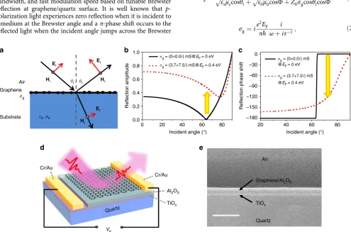
Physical model. The physical model is demonstrated in Fig. 1.
Figure1a shows the operation principle of the device. Graphene
with conductivity σgis placed on the dielectric silica substrate.
Light withp-polarization is incident from air onto the graphene/
silica medium. According to Maxwell’s equations, together with
the boundary conditions (Supplementary Note 1 and
Supple-mentary Figure 1), the reflection coefficient for p-polarization
light can be expressed by Eq. (1).
rp¼
ffiffiffiffiffiffiffiffi
εsμs
p cosθ
i ffiffiffiffiffiffiffiffiffiε0μ0
p cosΦþZ
0σgcosθicosΦ
ffiffiffiffiffiffiffiffi
εsμs
p
cosθiþ ffiffiffiffiffiffiffiffiffiε0μ0
p
cosΦþZ0σgcosθicosΦ
; ð1Þ
σg¼i
e2E F
πh i
ωþiτ1; ð2Þ
Graphene
g
Substrate
Air i r
Er
Hi
Et
Hr
Ei
Ht
0 20 40 60 80 20 40 60 80
Cr/Au
Cr/Au
Al2O3
Vg
TiOx
Quartz
Air
Graphene/Al2O3
TiOx
Quartz
s, s
1.0
0.8
0.6
0.4
0.2
0.0
Reflection amplitude
Incident angle (°) Incident angle (°)
Reflection phase shift
0
–30
–60
–90
–120
–150
–180
g = (0+0.0i) mS@EF = 0 eV
g = (3.7+7.5i) mS@EF = 0.4 eV
g = (0+0.0i) mS @EF = 0 eV
@EF = 0.4 eV
g = (3.7+7.5i) mS
a b c
d e
[image:2.595.50.546.377.704.2]where θi and Φ are the incident angle and refraction angle,
respectively;Z0is the impedance of air;εs,μsare the permittivity
and permeability of the silica substrate, and ε0,μ0are the
per-mittivity and permeability of air. We used the Drude model to describe the graphene conductivity, which can be expressed by Eq. (2)34,35. τ1¼ ev2
F
EFμc is the damping rate of carriers. In this
model, we use the ideal value of 10,000 cm2V−1s–1as the carrier
mobility μcof graphene36,37, and assume that the Fermi level of
the graphene, EF, ranges from 0.00 to 0.35 eV. vf is the Fermi
velocity andħis the reduced Planck constant. The parameters of
the substrate areεs=4 andμs=1. The modulation depth in this
model is defined as
MD¼ 1 j jr
2
rmax j j2
!
´100%; ð3Þ
where r is the reflection coefficient, and rmax is the baseline
defined as the maximum reflection value in this active system. As
an example here, we show the result at 0.8 THz.
Wefirst present the simulation results based on the physical
model in Fig.1a. When the Fermi level of graphene is at the Dirac
point, the conductivity of the graphene becomes the minimum. In
this case, Eq. (1) returns to the traditional Fresnel equation for
reflection. At the Brewster angle, the magnitude of reflection
intensity reaches zero, as shown in Fig. 1b. In addition, the
phase shift of reflection light is switched fromπto 0, when the
incident angle changes fromθi>θBtoθi<θB, as shown in Fig.1c.
While in the case of non-zero Fermi level, the Brewster
angle (defined as the incident angle that gives the smallest
reflffiffiffiffiffiffiffiffiection amplitude in this case) is shifted and determined by
εsμs
p cosθ
ipffiffiffiffiffiffiffiffiffiε0μ0cosΦZ0σgcosθicosΦ¼0, if ignoring the
imaginary part of graphene’s conductivity. The term introduced
by the conductivity,Z0σgcosθicosΦ, allows the Brewster angle to
be tunable. Because the conductivity of graphene is a complex
number, the reflection amplitude at the Brewster angle is not zero
(Fig.1b) and the phase changes gradually with the incident angle
close to the Brewster angle (Fig. 1c), which is a little different
from the abrupt change for conventional Brewster angle
reflection. As shown in Fig. 1, when the conductivity changes
from 0 to 3.7 mS, the Brewster angle shifts from 63 to 79°. When
the incident angle at 63° is fixed, the reflection amplitude
increases from 0 to ~0.52, as indicated by the yellow arrow in
Fig. 1b. In this case, the modulation depth is up to 100% due
to the perfect “off-state” (|r|=0, at 63°). The insertion loss of
this device, lg10 jrmaxj2
, is −5.6 dB. The insertion loss can be
reduced to −3 dB through using higher-quality graphene or
composing two-monolayer graphene (Supplementary Figure 2
and Supplementary Note 2). When the incident angle isfixed at
68°, a phase modulation range, as large as about 140°, can also be
achieved, as indicated by the yellow arrow in Fig. 1c.
The real device in this work is schematically shown in Fig.1d,
e. A graphene/Al2O3/TiOxsandwich structure is constructed for a
solid-state electrical gate to tune the conductivity of graphene (details of the fabrication can be seen in the Methods section). A
50-nm Al2O3 layer is used as a dielectric gate, which has a
negligible effect on the light reflection. The back gate electrode is
made of 10-nm thickness of a TiOx(sheet resistance ~2000Ω)
film. This thin and high-resistancefilm ensures the transparency
for the THz light. The transparency of TiOxis verified by THz
transmission spectrum and the loss of TiOxis also discussed in
Supplementary Figure 3 and Supplementary Note 3. The
properties of graphene are first characterized by atomic force
microscopy (AFM) for surface morphology with measurement of the thickness and also by Raman spectrum (Supplementary
Figure 4 and Supplementary Note 4). The tunability of graphene’s
conductivity through the electrical gate is tested by the device’s
THz transmission spectra (Supplementary Figure 5 and
Supple-mentary Note 5), as well as verified by a graphene field-effect
transistor (G-FET) (Supplementary Figure 6 and Supplementary Note 6).
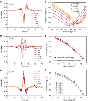
Actively controlled Brewster angle. In order to obtain the
Brewster angle of the device, we measured the reflected THz pulse
with an incident angle of 55–75°, as well as gate voltage from−12
to 12 V. Three typically reflected THz pulses in the time domain
are shown in Fig.2a–c. When the incident angle is 55°, the pulse
keeps an asymmetric “M”shape from −12 to 12 V. The pulse
amplitude decreases monotonically with the gate voltage. When
the incident angle is 68°, the pulse shape changed from “M”to
“W”, indicating a significant phase change during this process.
When the incident angle is 75°, the THz pulse keeps an
asym-metric“W”shape from−12 to 12 V and the amplitude decreases
monotonically. The pulse shape changing from “M” to “W”
indicates that the phase of THz wave is changed by 180°. We plot the curve of the amplitude as a function of incident angle under
different gate voltages in Fig. 2d (here the result of 0.8 THz is
taken as an example). The results for other frequencies are shown
in Supplementary Figure 7 and Supplementary Note 7. The“V”
curves show similar trends to the theoretical results (Fig.1b). To
verify our physical model, the conductivity of graphene is
extracted byfitting the experimental data to Eq. (1), as shown in
Fig.2d, and then the collected data are compared with the
con-ductivity extracted from transmission spectra (Supplementary
Figure S5). Thefitted conductivity increases from 0.3 to 2.2 mS,
and is consistent with the conductivity extracted from the device’s
THz transmission spectra (red curve of Fig.2e), as well as that
from G-FET (Supplementary Figure 6c). The fitting results for
other frequencies are shown in Supplementary Figure 7f, which is also consistent with that extracted from transmission spectra.
With the parameters extracted from fitting, the theoretical
reflection amplitude as a function of incident angle for the
fre-quency is achieved, as shown in Supplementary Figure 8 and
Supplementary Note 8. Figure 2f is the Brewster angle as a
function of gate voltage at different frequencies, and shows that the Brewster angle can be tuned from about 64.5 to 71.5°. The minute change in different frequencies is due to the weak dis-persion relation of conductivity in this frequency region. The passive tuning of Brewster angle by metamaterials and
metasur-face has been reported in previous works34,35. However, these
methods are hard to active tuning of Brewster angle. To change the Brewster angle, the unit structure or periodic parameter for the metamaterial or metasurface should be changed. Besides, Brewster angle of metamaterials/metasurface is always frequency-dependent, due to their resonance nature. As far as we know, this
work is thefirst time to realize an active tunable Brewster angle
and achieve broadband response.
Intensity modulator. From the result in Fig.2c, we observe that
a nearly zero reflection can be achieved at an incident angle of
65° when the gate voltage is 12 V. This indicates great potential to use our device as an intensity modulator with deep modulation
depth at this incident angle. Figure 3a shows the evolution of
the time-domain waveform reflected from the device as the
vol-tage changed from −12 to 14 V. The waveforms maintain a
similar shape, while the peak-to-peak value decreases from 1.37 to 0.067, indicating a nearly unchanged phase and a deeply
modu-lated intensity. The maximum reflected pulse is achieved when
the gate voltage is −12 V, and we define it as the baseline for
calculating the modulation depth. The reflection amplitude can
and Supplementary Note 9). The modulation depth of the
peak to peak is up to 99.7%, as shown in the inset of Fig.3a. By
Fourier transformation of each signal and comparing them to the baseline, a modulation depth of higher than 99.3% is
achieved over the frequency range of 0.5−1.6 THz and the
maximum modulation depth is 99.9%, indicating the broadband
and spectrally flat modulation. The high modulation depth
is due to the nearly zero reflection of THz light near the Brewster
angle. Experimental insertion loss of this intensity modulator is
about ~−12 dB (detailed calculation is shown in Supplementary
Note 2 and Supplementary Figure 2), which is comparable with or better than that of the high-performance narrow bandwidth
metadevices38–40. This experimental insertion loss is mainly
due to the poor quality of commercial graphene and the fabri-cation process.
In order to further clarify this phenomenon, we simulated the
electric field distribution at the frequency of 0.8 THz, when
graphene’s conductivity is 0.5 and 3.5 mS, corresponding to the
gate voltage of 14 and −12 V in the experiment. As shown in
Fig.3c, when the conductivity is low (0.5 mS), the incident angle
is very close to the Brewster angle of the device, which results in a
very weak reflection being observed. While graphene’s
conduc-tivity is 3.5 mS, the Brewster angle is moved far away from the
current incident angle, as shown in Fig. 2c. This results in a
considerably strong reflectionfield, as illustrated in Fig.3d. The
fitted reflection amplitude as a function of gate voltage shows a
high degree of matching with our theoretical results, as well as experimental results (as shown in Supplementary Figure 10 and Supplementary Note 10).
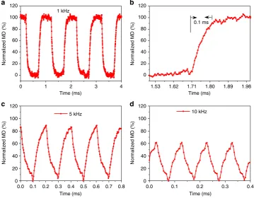
The performance of the device, both of the modulation depth and operation band, is much higher than that of previous results6–13,23–30,41–43. More importantly, owing to the solid-state-based modulations, our device provides a high modulation
speed, as shown in Fig.4a. The rising time of modulation is about
0.1 ms, as shown in Fig. 4b, corresponding to the modulation
speed of about 10 kHz. When the modulation speed is up to
8 10 12 14 16 18
12 V 8 V 4 V 0 V –4 V –8 V –12 V
64 66 68 70 72
4 10 12 14
Amplitude
Conductivity (m
S)
Brewster angle (
°)
–10 –5 0 10 15
54 57 60 63 66 69 72 75 0.00
0.02 0.04 0.06 0.08 0.10
12 V 8 V 4 V 0 V
–12 V –8 V
a
b
c
d
e
f
0.8
0.4
0.0
–0.4
–0.8
–1.2
–1.6
–2.0
Amplitude
0.4 2.5
2.0
1.5
1.0
0.5
0.0 0.2
0.0
–0.2
–0.4
–0.6
1.2
0.8
0.4
0.0
–0.4
–0.8
Amplitude
Reflection amplitude
Time (ps) Incident angle (°)
6 8
Time (ps) Gate voltage (V)
5 –15
4 6 8 10 12 14 –10 –5 0 10 15
Time (ps) Gate voltage (V)
5 –15
i = 55°
i = 68°
i = 75°
–4 V
12 V 8 V 4 V 0 V –4 V –8 V –12 V
Fitting from breswter angle Extracting from transmission spectrum
12 V 8 V 4 V 0 V –4 V –8 V
–12 V 0.4 THz
0.6 THz 0.8 THz 1.0 THz 1.2 THz 1.4 THz
[image:4.595.110.486.49.476.2]5 and 10 kHz, the modulation depth decreases to 80% and 60%,
respectively, as shown in Fig.4c, d. Theoretically, the modulation
speed of a solid-state dielectric-gating device is limited by the
resistance–capacitance (RC) time constant. In our device, the
effective series resistance (R) comes from the graphene and TiOx.
Here, we take a resistance of 250Ωfor the graphene and 1000Ω
for the TiOx, which are calculated by the half of averaged
square resistance over the gate voltage range. A capacitance (C) of
~140 nF is calculated by adopting a 50-nm Al2O3 and an active
device (graphene) area of 1.0 × 1.0 cm. Therefore, the calculated
6 10 12 14
Amplitude
1 6V 14 V 12 V 8 V 4 V 0 V –4 V –8 V –12 V
0.2 0 20 40 60 80 100
120 16 V 12 V 8 V 4 V
0 V –4 V –8 V
Quartz –1 Quartz
1
–1 1 –12 –8 –4 4 12 16
0 20 40 60 80 100
Modulation depth (%)
0.6
0.3
0.0
–0.3
–0.6
–0.9
8
Time (ps) Frequency (THz)
0.4 0.6 0.8 1.0 1.2 1.4 1.6
s = 0.5 mS @ Vg = 12 V s = 2.5 mS @ Vg= –12 V
Air Air
1.5 1.2 0.9 0.6 0.3 0.0
Peak to peak
Modulation depth
0 8 Gate voltage (V)
a b
c d
Fig. 3The device operates as a THz intensity modulator, when the incident angle is 65°.aReflected THz signal in a time domain.bThe modulation depth as a function of frequency. The simulatedE-field with a conductivity of (c) 0.5 mS, and (d) 2.5 mS under the incident angle of 65°. The dashed line presents the graphene on quartz
0.1 0.3
10 kHz 5 kHz
1.53 1.62 1.71 1.80 1.89 1.98
0 1 2 3 4
0 20 40 60 80 100 120
1 kHz
Normalized MD (%)
0 20 40 60 80 100 120
Normalized MD (%)
0 20 40 60 80 100 120
Normalized MD (%)
0 20 40 60 80 100 120
Normalized MD (%)
Time (ms)
0.4
0.0 0.2
0.1 0.3 0.4 0.5 0.6 0.7 0.8 0.0 0.2
Time (ms) Time (ms)
Time (ms)
0.1 ms
a b
c d
[image:5.595.115.478.50.303.2] [image:5.595.117.477.362.642.2]RC time constant is 1.75 × 10⁻⁴S, corresponding to a modulation
speed of ~6 kHz, which agrees well with the experimental result. Higher modulation speed (shorter RC time constant) can
be realized through replacing TiOx by a higher-conductivity
material (e.g., graphene) and reducing the device size. For
instance, by utilizing graphene to replace TiOx and reducing
the device size to ~1.0 × 1.0 mm (about two times the wavelength of 0.8 THz), the modulation speed will be ~2.4 MHz, which is comparable with other solid-state THz modulators in previous reports4,7,24,27.
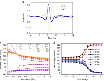
Phase modulator. According to the physical model, a broadband
phase modulation with a deep modulation range can be achieved by utilizing the phase-jump property across the Brewster angle. Here, we chose the incident angle of 68° to discuss this issue. The
reflected THz time-domain signal changes from an asymmetry
“W” shape at the gate voltages of 16 V to an asymmetry “M”
shape at the gate voltages of –12 V, which indicates that there
should be a large phase shift from Vg=16 V toVg=−12 V, as
shown in Fig. 5a. The phase shift in the frequency domain is
extracted from the time-domain pulse by Fourier transform and referenced to the phase at a gate voltage of 16 V, as shown in
Fig.5b. Over the broad frequency range from 0.5 to 1.6 THz, as
the gate voltage decreased from −8 to 16 V, the relative phase
shift decreases monotonically with a modulation range over 140°, showing that an ultra-broadband and deep phase modulation is achieved, which is highly consistent with our simulation results. We also noticed that there is a relatively larger modulation range
at low frequencies (e.g.,–180° at 0.4 THz) and a relatively smaller
modulation range at high frequencies (e.g., 140° at 1.6 THz). This frequency dependency is expected to contribute to the frequency-dependent imaginary conductivity of graphene described by the Drude model (Supplementary Note 11 and Supplementary Figure 11).
Discussion
In this work, THz modulation-based graphene-controlled
Brew-ster angle device is experimentally demonstrated for thefirst time.
The device is fabricated using a graphene/Al2O3/TiOxsandwich
structure on a quartz substrate. The conductivity of the graphene can be electrically controlled to generate a variable Brewster angle. Based on this device, an ultra-broadband THz-intensity modulator with a modulation depth larger than 99.3% and an ultra-broadband-phase modulator with a tunability higher than 140° are demonstrated. Our work presents graphene-controlled Brewster angle device for ultra-broadband THz intensity and phase modulation at room temperature. The promising perfor-mance of our device also suggests that there exists a great potential to use graphene in deliberate architecture for active THz devices.
Methods
Device fabrication. A Tifilm of 8 nm was deposited on a quartz substrate (diameter of 2 cm) for the bottom-gate electrode. In order to avoid further reducing the conductivity of Ti, the Tifilm was oxidized into TiOxthrough
annealing at 150 °C. After oxidization, the conductivity of thisfilm was about a reciprocal of sheet resistance of 2000Ω, which was measured using a four-probe method. Then, a layer of Al2O3(50 nm) was deposited by atomic layer deposition
onto TiOxas a dielectric gate. Afterward, graphene (~1 × 1 cm) was transferred
onto the as-prepared quartz/TiOx/Al2O3substrate. Subsequently, two electrodes
(Cr/Au) were fabricated by thermal deposition. One was on graphene and the other one was on TiOxfor the gate voltage. The device is schematically shown
in Fig.1f.
Measurements. A THz-TDS system from Menlo Systems (TERA-K15) was used for the terahertz reflection measurements. A reflection guide was used for manual adjustment of the reflection angle, ranging from a minimal reflection angle of 55 to 75°.
Data availability
All data supporting thefindings of this study are available within the article and its Supplementary Information. All other data are available from the corresponding author upon reasonable request.
0.4 0.8 1.2 1.6
–40 0 40 80 120 160 200 240
280 14 V 12 V 10 V 8 V
6 V 4 V 2 V 0 V
–2 V –4 V –6 V –8 V
–10 V –12 V
4 10 12 14
–0.6 –0.4 –0.2
16 V –12 V
–10 –5 5 10 5
0 40 80 120 160 200 240 280 320 360
Relative phase shift (°) Relative phase shift
0.2 0.6 1.0 1.4
Frequency (THz) Gate voltage
0
0.25 THz 0.4 THz 0.6 THz 0.8 THz 1.0 THz 1.2 THz 1.4 THz
6 8
Time (ps)
Amplitude
0.0 0.2 0.4
a
b c
[image:6.595.118.482.49.331.2]Received: 20 March 2018 Accepted: 25 October 2018
References
1. Chan, W. L., Deibel, J. & Mittleman, D. M. Imaging with terahertz radiation. Report. Progress. Phys.70, 1325 (2007).
2. Han, P. Y., Cho, G. C. & Zhang, X.-C. Time-domain transillumination of biological tissues with terahertz pulses.Opt. Lett.25, 242 (2000).
3. Koenig, S. et al. Wireless sub-THz communication system with high data rate. Nat. Photonics7, 977 (2013).
4. Rahm, M., Li, J.-S. & Padilla, W. J. THz wave modulators: a brief review on different modulation techniques.J. Infrared Millimetre Terahertz Waves34, 1–27 (2013).
5. Nagatsuma, T., Ducournau, G. & Renaud, C. C. Advances in terahertz communications accelerated by photonics.Nat. Photonics10, 371–379 (2016). 6. Chen, H.-T. et al. Active terahertz metamaterial devices.Nature444, 597 (2006). 7. Chen, H.-T. et al. A metamaterial solid-state terahertz phase modulator.Nat.
Photonics3, 148 (2009).
8. Chen, H.-T. et al. Experimental demonstration of frequency-agile terahertz metamaterials.Nat. Photonics2, 295 (2008).
9. Cui, Y. et al. Ultrabroad-band light absorption by a saw-tooth anisotropic metamaterial slab.Nano Lett.12, 1443 (2012).
10. Gu, J. et al. Active control of electromagnetically induced transparency analogue in terahertz metamaterials.Nat. Commun.3, 1151 (2012). 11. Liu, X., Hu, X., Yang, H. & Gong, Q. Ultralow-power all-optical tunable
double plasmon-induced transparencies in nonlinear metamaterials.Appl. Phys. Lett.100, 131101 (2012).
12. Cao, W. et al. Plasmon-induced transparency in metamaterials: active near
field coupling between bright superconducting and dark metallic mode resonators.Appl. Phys. Lett.103, 101106 (2013).
13. Liu, P. Q. et al. Highly tunable hybrid metamaterials employing split-ring resonators strongly coupled to graphene surface plasmons.Nat. Commun.6, 8969 (2015).
14. Novoselov, K. S. et al. Electricfield-effect in atomically thin carbonfilms. Science306, 666 (2004).
15. Castro Neto, A. H., Guinea, F., Peres, N. M. R., Novoselov, K. S. & Geim, A. K. The electronic properties of graphene.Rev. Mod. Phys.81, 109 (2009). 16. Novoselov, K. S. et al. Two-dimensional gas of massless Dirac fermions in
graphene.Nature438, 197 (2005).
17. Das Sarma, S., Adam, S., Hwang, E. H. & Rossi, E. Electronic transport in two dimensional graphene.Rev. Mod. Phys.83, 407 (2011).
18. Li, X. et al. Graphene and related two-dimensional materials: structure-property relationships for electronics and optoelectronics.Appl. Phys. Rev.4, 021306 (2017).
19. Gan, X. et al. Chip-integrated ultrafast graphene photodetector with high responsivity.Nat. Photonics7, 883 (2013).
20. Rouhi, N. et al. Terahertz graphene optics.Nano Res.5, 667 (2012). 21. Tassin, P., Koschny, T. & Soukoulis, C. M. Graphene for terahertz
applications.Science6146, 620 (2013).
22. Yan, H. et al. Tunable infrared plasmonic devices using graphene/insulator stacks.Nat. Nanotechnol.7, 330 (2012).
23. Low, T. & Avouris, P. Graphene plasmonics for terahertz to mid-infrared applications.ACS Nano8, 1086 (2014).
24. Sensale-Rodriguez, B. et al. Broadband graphene terahertz modulators enabled by intraband transitions.Nat. Commun.3, 780 (2012).
25. Lee, S. H. et al. Switching terahertz waves with gate-controlled active graphene metamaterials.Nat. Mater.11, 936 (2012).
26. Liang, G. et al. Integrated terahertz graphene modulator with 100% modulation depth.ACS Photonics2, 1559 (2015).
27. Ju, L. et al. Graphene plasmonics for tunable terahertz metamaterials. Nat. Nanotechnol.6, 630 (2011).
28. Li, Q. et al. Active graphene–silicon hybrid diode for terahertz waves. Nat. Commun.6, 7082 (2015).
29. Weis, P. et al. Spectrally wide-band terahertz wave modulator based on optically tuned graphene.ACS Nano6, 9118 (2012).
30. Miao, Z. et al. Widely tunable terahertz phase modulation with gate-controlled graphene metasurfaces.Phys. Rev. X5, 041027 (2015).
31. Thareja, V. et al. Electrically tunable coherent optical absorption in graphene with ion-gel.Nano Lett.15, 1570 (2015).
32. Jiang, L., Wang, Q., Xiang, Y., Dai, X. & Wen, S. Electrically tunable Goos–Hänchen, shift of light beam reflected from a graphene-on-dielectric surface.IEEE Photonics J.5, 6500108 (2013).
33. Bludov, Y. V., Peres, N. M. R. & Vasilevskiy, M. I. Unusual reflection of electromagnetic radiation from a stack of graphene layers at oblique incidence. J. Opt.15, 114004 (2013).
34. Horng, J. et al. Drude conductivity of Dirac fermions in graphene.Phys. Rev. B 83, 165113 (2011).
35. Hansona, G. W. Dyadic Green’s functions and guided surface waves for a surface conductivity model of graphene.J. Appl. Phys.103, 064302 (2008).
36. Li, X. et al. Graphenefilms with large domain size by a two-step chemical vapour deposition process.Nano Lett.10, 4328 (2010).
37. Kim, S. M. et al. Synthesis of large-area multilayer hexagonal boron nitride for high material performance.Nat. Commun.6, 8662 (2015).
38. Tamayama, Y., Nakanishi, T., Sugiyama, K. & Kitano, M. Observation of Brewster’s effect for transverse-electric electromagnetic waves in metamaterials: experiment and theory.Phys. Rev. B73, 193104 (2006). 39. Alù, A. et al. Plasmonic Brewster angle: broadband extraordinary transmission
through optical gratings.Phys. Rev. Lett.106, 123902 (2011). 40. Paniagua-Domínguez, R. et al. Generalized Brewster effect in dielectric
metasurfaces.Nat. Commun.7, 10362 (2016).
41. Sensale-Rodriguez, B. et al. Extraordinary control of terahertz beam reflectance in graphene electro-absorption modulators.Nano Lett.9, 4518 (2012).
42. Balci, O. et al. Electrically switchable metadevices via graphene.Sci. Adv.1, eaao1749 (2018).
43. Kim, T.-T. et al. Electrical access to critical coupling of circularly polarized waves in graphene chiral metamaterials.Sci. Adv.3, e1701377 (2017).
Acknowledgements
The work is in part supported by Research Grants Council of Hong Kong, particularly, via grant nos. 14207515, 14201415, 14204616, AoE/P-02/12, Hong Kong SAR Govern-ment, and CUHK Group Research Scheme, the Hong Kong Innovation and Technology Fund (project number ITS/371/16), and the Royal Society Wolfson Merit Award (E.P.-M.). J.-B.X. would like to thank the National Science Foundation of China for the support, particularly, via grant no. 61229401.
Author contributions
Z.C. and J.-B.X. conceived the concept. Z.C. fabricated the devices, conducted the measurements, and analyzed the data. X.C. established the experimental setup and conducted the measurements, and contributed to the analysis. L.T., K.C., M.L., K.Y. and X.L. assisted in the fabrication and data analysis. R.I.S. developed and instructed the modulation speed measurement program. J.-B.X. and E.P.-M. supervised the work. All the authors discussed the work.
Additional information
Supplementary Informationaccompanies this paper at https://doi.org/10.1038/s41467-018-07367-8.
Competing interests:The authors declare no competing interests.
Reprints and permissioninformation is available online athttp://npg.nature.com/ reprintsandpermissions/
Publisher’s note:Springer Nature remains neutral with regard to jurisdictional claims in published maps and institutional affiliations.
Open Access This article is licensed under a Creative Commons Attribution 4.0 International License, which permits use, sharing, adaptation, distribution and reproduction in any medium or format, as long as you give appropriate credit to the original author(s) and the source, provide a link to the Creative Commons license, and indicate if changes were made. The images or other third party material in this article are included in the article’s Creative Commons license, unless indicated otherwise in a credit line to the material. If material is not included in the article’s Creative Commons license and your intended use is not permitted by statutory regulation or exceeds the permitted use, you will need to obtain permission directly from the copyright holder. To view a copy of this license, visithttp://creativecommons.org/ licenses/by/4.0/.