go.warwick.ac.uk/lib-publications
Original citation:
Challa, Pavan K., Kartanas, Tadas, Charmet, Jérôme and Knowles, Tuomas P. J.. (2017)
Microfluidic devices fabricated using fast wafer-scale LED-Lithography patterning.
Biomicrofluidics.
Permanent WRAP URL:
http://wrap.warwick.ac.uk/85798
Copyright and reuse:
The Warwick Research Archive Portal (WRAP) makes this work by researchers of the
University of Warwick available open access under the following conditions. Copyright ©
and all moral rights to the version of the paper presented here belong to the individual
author(s) and/or other copyright owners. To the extent reasonable and practicable the
material made available in WRAP has been checked for eligibility before being made
available.
Copies of full items can be used for personal research or study, educational, or not-for profit
purposes without prior permission or charge. Provided that the authors, title and full
bibliographic details are credited, a hyperlink and/or URL is given for the original metadata
page and the content is not changed in any way.
Publisher’s statement:
This article may be downloaded for personal use only. Any other use requires prior permission of the author and AIP Publishing.
The following article has been accepted by Biomicrofluidics. After it is published, it will be found at http://aip.scitation.org/journal/bmf/
A note on versions:
The version presented here may differ from the published version or, version of record, if
you wish to cite this item you are advised to consult the publisher’s version.
patterning
Pavan K. Challa,1Tadas Kartanas,1J´erˆome Charmet,1, 2,a)and Tuomas P. J. Knowles1, 3,a)
1)
Department of Chemistry, University of Cambridge, Lensfield Road, Cambridge, CB2 1EW, UK.
2)Institute of Digital Healthcare, WMG, University of Warwick, Coventry, CV4 7AL, UK.
3)
Cavendish Laboratory, Department of Physics, University of Cambridge, JJ Thomson Avenue, Cambridge CB3 0HE, UK.
(Dated: 14 January 2017)
Current lithography approaches underpinning the fabrication of microfluidic devices rely on UV exposure of photoresists to define microstructures in these materials. Conventionally, this objective is achieved with gas discharge mercury lamps which are capable of producing high intensity UV radiation. However, these sources are costly, have a comparatively short lifetime, necessitate regular calibration, and require significant time to warm up prior to exposure taking place. To address these limitations in this paper we exploit advances in solid state sources in the UV range and describe a fast and robust wafer-scale laboratory exposure system relying entirely on UV-LED illumination. As an illustration of the potential of this system for fast and low-cost microfluidic device production, we demonstrate the microfabrication of a 3D spray-drying microfluidic device and a 3D double junction microdroplet maker device.
I. INTRODUCTION
Photolithography techniques that rely on transferring small scale structures from photomasks onto flat sub-strates using light represent one of the main fabrication routes in microelectronics and micro-devices1,2, including microfluidics3–5. Generally, radiation in the UV range is used to activate photoresists and the illumination is achieved commonly with gas-discharge lamps using mer-cury vapour. Such sources produce a wide spectrum of light and are coupled with filters to select the desired wavelength. Appropriate optics can then be used to col-limate the light over the entire exposure area. However, such lamps require significant time to warm up, have a limited life time of typically 2000 hours for laboratory sources and require regular calibration.
In an attempt to optimise the laboratory scale fab-rication of microfluidic devices, we have explored solu-tions to simplify the photolithography step by exploit-ing progress in solid-state LED sources operatexploit-ing in the UV range. There are several requirements for a effective and accurate UV exposure source for lithography applica-tions. Firstly, the light used for photolithography should be uniform ove a wafer scale to maintain compatibility with standard wafer substrates and to ensure that each area is exposed to same dose of energy. Secondly, the emission spectrum should have a small bandwidth since the absorption in the photoresist is wavelength depen-dent. Lastly, the illumination should be well collimated to ensure sharply defined features in the fabricated mi-crostructures. All of these features can be achieved us-ing light emittus-ing diodes (LEDs) and UV transparent
a)Authors to whom correspondence should be addressed.
Elec-tronic addresses: [email protected] and [email protected]
optical lenses. LEDs possess clear advantages over mer-cury lamps as they consume less electricity, they can be turned on and off within seconds, their life time is 20,000 hours, and they are cheap and extremely simple to use. However, until recently, the main limitation was their low power in the UV spectrum which hindered their rou-tine use for photolithography applications. This techni-cal limitation has been overcome by assembling several LED’s into arrays6–9. As such, new generation LED light sources have a high power source with integrated heat sink to keep the power at stable values, allowing their use for photolithography. We combine the exposure system with a micrometer positioning stage to allow multilayer lithography to be performed.
In view of the considerations above, we present here a highly versatile lab-scale UV-LED based photolithogra-phy set-up, with a mask aligner comprised of micrometric XYZ and rotation stages. The set-up addresses the main issues of conventional mercury lamp based mask aligners while retaining the resolution required for conventional microfluidic applications. In this paper we describe the entire set-up in section II and its characterisation in sec-tion III. We show some examples of the features obtained, and in particular, we show PDMS based microfluidic de-vices fabricated with the set-up in section IV.
II. UV-LED LITHOGRAPHY PLATFORM
2
FIG. 1. Description of the system. A) Photograph of the UV-LED lithography platform describing the main components used in the platform, B) Schematic of the Optical set-up.
A. Optical set-up
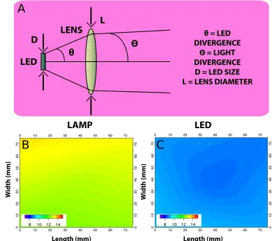
The UV-LED(Thorlabs M365LP1) outputs maximum power of about 1000 mW when driven by LED Driver (Thorlabs LEDD1B) set on external trigger mode sup-plied with a constant current of 1.2 amperes. The LED is triggered by a general purpose input/output (GPIO) pin from a Raspberry Pi 3 single board computer, con-nected to a 7 inch Touchscreen Monitor for user input and control (see Fig. 1 for details). A custom python based graphical user interface (GUI) was developed that allows the user to change the exposure time and start the illumination. An emergency stop button was also in-cluded. Even though Python is not a real-time program-ming language, variability in the tiprogram-ming of the order of 1ms characteristic of such systems, does not represent an issue for exposure times in the range of seconds. In the platform, the LED is positioned 210 mm from the bot-tom exposure area (table level) and the lens is positioned 60 mm from the LED (Fig.1). For single layer pattern-ing, when no alignment is necessary, the wafer is posi-tioned on the bottom exposure plane, but it is mounted on the 90 mm high mask aligner when relative alignment of multiple features is necessary. To ensure good resolu-tion, it is crucial that the beam is collimated. In order to collimate the diverging light from the LED, we use an aspheric condenser lens of focal length 60 mm (Thorlabs ACL7560U) as shown in Fig.2A. Geometric constraints imply that the divergence angle of light after the lens Θ can be approximated by the relation Θ=θD/L, where D is the size of the LED active area,θ, the LED divergence angle and L is the diameter of the collimating lens. This factor plays a role in the level of collimation that effects the resolution of the exposure system. For our platform this value [≈0.023 rad] is comparable with commercial gas discharge mercury lamp based photolithography sys-tems.
In order to characterise the uniformity of the illumi-nation on a waver scale, we measured the intensity using a detector (Thorlabs S401C) connected to a power me-ter (Thorlabs PM100A). The power of the light source is
W
idth (mm)
LAMP LED
D LED
LENS
L
= LED DIVERGENCE
= LIGHT DIVERGENCE D = LED SIZE L = LENS DIAMETER
Length (mm) Length (mm)
W
idth (mm)
A
B C
FIG. 2. A) Figure illustrates the divergence angle of the LED after the collimating lens, B) 2D map of lamp intensity, C) 2D map of LED intensity at the wafer surface for a fixed height of 15cm from the platforms.
a important parameter which defines the radiation dose that the photoresist is exposed to. Irradiance, the light energy at the wafer surface has to be calculated to opti-mise the curing conditions and the light source has thus in general to be calibrated to achieve reproducible re-sults. In the case of a mercury lamp, the intensity de-creases over the life time of the lamp whereas it remains appreciably constant for a LED. Upon calibration of our system using the maximum power of the LED driver -we have evaluated the uniformity of the beam by posi-tioning the detector over the active exposure area (ap-proximately 100 mm2) and compared the results with a conventional mercury lamp (Optical Associated Inc., 200 Watts NUV). Figure 2B and C shows the power map (measured in mW) obtained on the active area. In this case, the detector was 150 mm away from the light source. Our results show that the uniformity in the irradiance is comparable between the LED system and the commer-cial mercury vapour based system. In particular, the exposure area achieved using our approach is sufficient to uniformly expose a standard 3 inch wafer. The colli-mation of the beam was also checked by measuring the beam diameter at different heights (40 and 80 mm from the wafer level) and no major differences were observed.
B. Mask aligner
To allow the use of the exposure source for multi-layer lithography, we combine it with a mask aligner. The mask aligner consist of micrometric X-Y-Z and rotation stages and a holder for a quartz window as shown in Fig. 3.A. The mask alignment procedure consists of 4 steps (Fig 3A-C), described below:
[image:3.612.340.535.54.227.2]A
Alignment MarksB
C
[image:4.612.82.533.53.202.2]First layer of device
Second layer of device
UV - LED Exposure
FIG. 3. Schematic of the mask aligner for lab-scale exposure system, and the alignment process. Mask alignment steps to make multilayer devices: A) Silicon wafer with cured structures and alignment marks is attached onto the XYZ,θstage , B) Alignment marks on photomask attached to quartz plate are aligned by adjusting the translating and rotation knobs of the XYZ,θstage, and C) Expose the wafer with UV-LED light.
stage. The wafer is held in place at the centre of the stage using vacuum grease.
2.Placement of the mask on the wafer. The acetate mask with the features to be transferred is taped to the quartz window. The window is brought into contact with the wafer by sliding it along the vertical posts. The window is clamped into place. Note, for higher resolution features, a chrome mask could also be used instead of the ac-etate mask tapped onto a quartz window.
3.Positioning of the mask on the wafer. The micrometer stage is brought down (Z-axis) so that the mask is not in contact with the wafer any more and the X-Y and rotation stages are adjusted to align the registrations marks. The positioning takes place under a binocular. Once the alignment is satisfactory, the Z-stage is brought back up into contact with the quartz window.
4.Exposure. Once the alignment steps are com-pleted, the mask aligner is brought under the UV-LED for exposure. After exposure, the Z-stage is brought back down and the quartz window removed to release the wafer. The vacuum grease is removed from under the wafer before further processing.
III. CHARACTERISATION OF THE SET-UP
In this section, we discuss the characterisation of the set-up and show that the features obtained compare well with those obtained using a conventional mercury lamp, but with the advantages of low-cost, convenient and re-liable operation characteristic of LED sources. To vali-date the performance of the UV-LED lithography plat-form, we have micro-fabricated structures into the nega-tive SU8 3000 series(Microchem) i-line photoresist. The
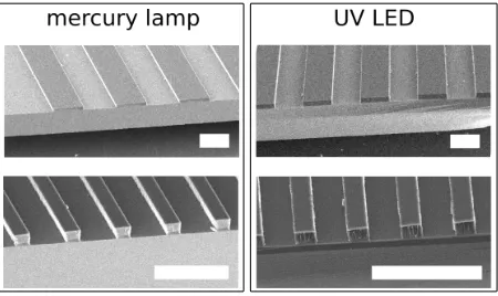
FIG. 4. Comparison of SU8 structures obtained using a con-ventional mercury lamp and a LED. The SEM micrographs show channels (100µm and 20 µm wide of 20 µm height) fabricated using each light source. The scale bar is 100µm.
photoresist is spun onto a silicon wafer and soft baked ac-cording to the manufacturer’s protocols. The photomask with the desired patterns is then placed on the wafer and the whole assembly is positioned under our home built LED-lithography platform. Upon exposure, the UV light crosslinks the exposed SU8 photoresist and the un-exposed SU8 is dissolved using appropriate solvents dur-ing the development step. After the post exposure bake, the SU8 patterns are visible on the wafer. The patterns obtained using our set-up were examined using Scanning Electron Microscope and compared with patterns gener-ated using a gas discharge mercury lamp.
[image:4.612.328.553.284.418.2]4
200 um
A [image:5.612.55.299.52.264.2]B C
FIG. 5. Evaluation of SU8 features obtained using the UV LED. The scale bar of the SEM micrographs is 200µm. A) Structures of 25 µm height obtained after a 21 s exposure time at full poser. B) details of the structures shown in (A). C) High aspect ratio structures (100µm high, 20µm wide) obtained after a 40 s exposure time at full power.
A
C
B
D
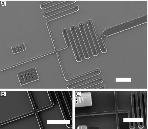
FIG. 6. SEM micrographs of features obtained using a two layer photolithography process. A) and B) show PDMS replica of well aligned channels obtained using the alignment procedure detailed in the paper. C) image of droplet maker device. D) water-ethanol droplets were formed using a block-copolymer surfactant. The scale bar is 100µm.
of the photolithography process. Resolution of features formed through exposure through acetate film masks is commonly limited by the resolution of the printing of the masks themselves, which is commonly of the order of 5-10µm. However, this can be improved by the use of chrome masks provided the application requires better resolutions. Level of collimation of the light source plays a key role in the resolution of an exposure system. For our system, assuming feature size of the mask to be S,
then the change in size ∆S due to the level of collima-tion is given by ∆S=2dtan(Θ), where dis the distance between wafer and mask, and Θ is the divergence angle of the light. For our system the values are 1 µm and 4
µm for resist thickness of 25µm and 100µm. These are the typical values that are obtained with lamp based sys-tems. Figure 4 shows a comparison between structures obtained using a mercury lamp and an LED. Considera-tion of the micrographs reveals that the structures (100
µm and 20µm wide channels of 20µm height) are com-parable.
[image:5.612.56.298.358.520.2]The resolution of the printing on the acetate mask is visible at these scales through slight corrugations in the sides of the channels, both in the UV-LED exposed de-vices as well as the ones produced using conventional mercury lamp illumination. Channels with higher reso-lutions could be obtained using high-resolution chrome mask. The features in Fig. 5.C are typical of under ex-posure on the 20µm wide channels. In particular, it can be seen that the channels are wider at the top of the structure than at the bottom. This image reveals that the mercury lamp used for the experiment needs calibra-tion as its intensity has decreased significantly since the last time it was calibrated. On the other hand, an LED, whose output is largely constant throughout its lifetime does not require frequent calibration. It can therefore be expected that, under the same conditions, we will obtain more readily the vertical wall structures observed in Fig. 4 with the UV LED set-up.
Figure 5 shows typical SU8 structures of droplet maker devices (see10,11 for examples of experiments exploit-ing this technology) obtained with the UV LED set-up. Structures of 25µm height, obtained using a 21 s expo-sure at full power are shown in Fig. 5.A and Fig. 5.B. It can be seen that the structures are well resolved in this case and compare well with features obtained using con-ventional mercury lamps (see Fig 4). In order to verify the efficiency of the system, we have tested high aspect ratio structures. Channels of 20 µm width and 100 µm height can be seen in Fig. 5.C. In this case, a 40 s ex-posure time at full power was necessary to obtain well resolved features. Shorter exposure time (and hence a lower UV dose) resulted in thinner structure that col-lapsed under their own weight (not shown). If SU8 is underexposed, it is slightly softer12 and, therefore, the structure may collapse. The hard baking time has to be longer than usual to attain a reasonable strength. The height of the 100µm channels is best seen from the col-lapsed evaluation feature at the bottom of the image.
IV. MICROFLUIDIC DEVICES
fill-ing the channels with the solution as received and sub-sequently washing them with isopropanol prior to the experiments to remove the debris. The treatment im-proved the wetting of the channels with fluorinated oil13. Ethanol and water solutions were mixed on chip to form a solution of 10% (v/v) ethanol in water, and micro-droplets were formed in an oil phase of Fluorinert FC-40 (Sigma-Aldrich) and 2.0% (w/w) block-copolymer sur-factant. Such two component mixer on chip devices have been previously used to study peptide self-assembly14,15. Fig.6.B shows the droplet maker while in operation and the two phase mixing within the droplet. As a second ex-ample, we have fabricated a non-planar microfluidic de-vice with a 3D junction. By exploiting the alignment pro-cedure described above, we fabricated two layer lithogra-phy masters for the replication of PDMS devices. Figure 6 C,D shows an example of a PDMS replica layer ob-tained from a master fabricated using a two mask process. The first side of a two-layer 3D flow focusing device is in nature very similar to devices which have been previously used to produce double emulsion droplets13. The micro-graph (Fig. 6.C,D) shows that the thin (20µm wide, 25
µm high) channel is well positioned with respect to the thick channels (50 µm wide, 50 µm high). The rugged edges seen on the PDMS replica are due to the low reso-lution of the acetate masks. Additional irregularities can be due to the fact that we have a 2-layers master. In this case, it is more difficult to remove uncured photore-sist (from the second layer) during the development step. This situation is clearly seen at the intersection between the small and large channels in (Fig. 6.D). It can also be observed with conventional mask aligners/lamps. In addition, such variations do not affect significantly the performance of the microfluidic device in the cases pre-sented since we are operating in a laminar regime. In case an application requires higher resolution channels, a high-resolution mask should be chosen. Taken together, these results demonstrate the potential of our LED expo-sure system for single and double layer UV lithography.
V. CONCLUSIONS
Photolithography, a common patterning technique used in microfabrication, traditionally relies on the use of
gas discharge mercury lamps with limited reliability and lifetime. In this paper we have presented a simple and robust photolithography set-up, comprised of a UV-LED platform with micrometric positioning stages. The res-olution of the features obtained by the platform match that of those required for microfluidics applications. In addition, the system does not suffer from the drawback of conventional gas discharge lamps used in mask align-ers that need frequent calibration. The use of LEDs, al-lows for a robust and reliable processing. The alignment procedure presented, here by using a combination of mi-crometric positioning stage, was used to produce 2 layer masters. Using soft-lithography, we have reproduced the negative features into PDMS and shown that the devices compare well with devices obtained using a conventional mercury lamp and mask aligner. In summary, LED expo-sure platforms have the potential to provide the basis for reliable, robust micrometer size lithography applications.
1J. Bryzek, K. Peterson, and W. McCulley, IEEE Spectrum31,
20 (1994).
2C. R. Barrett, MRS Bulletin18, 3 (1993).
3Y. Xia, , and G. M. Whitesides, Annual Review of Materials
Science28, 153 (1998).
4D. C. Duffy, J. C. McDonald, O. J. A. Schueller, and G. M.
Whitesides, Analytical Chemistry70, 4974 (1998).
5Y. Xia and G. M. Whitesides, Angewandte Chemie International
Edition37, 550 (1998).
6M. K. Yapici and I. Farhat, Proc. SPIE9052, 90521T (2014). 7M. D. Huntington and T. W. Odom, Small7, 3144 (2011). 8R. M. Guijt and M. C. Breadmore, Lab Chip8, 1402 (2008). 9S. Suzuki and Y. Matsumoto, Microsystem Technologies14, 1291
(2008).
10S. Mashaghi, A. Abbaspourrad, D. A. Weitz, and A. M. van
Oijen, TrAC Trends in Analytical Chemistry82, 118 (2016).
11T. P. J. Knowles, D. A. White, A. R. Abate, J. J. Agresti, S. I. A.
Cohen, R. A. Sperling, E. J. De Genst, C. M. Dobson, and D. A. Weitz, Proceedings of the National Academy of Sciences 108, 14746 (2011).
12M. B. Chan-Park, J. Zhang, Y. Yan, and C. Yue, Sensors and
Actuators B: Chemical101, 175 (2004).
13S. Koster, F. E. Angile, H. Duan, J. J. Agresti, A. Wintner,
C. Schmitz, A. C. Rowat, C. A. Merten, D. Pisignano, A. D. Griffiths, and D. A. Weitz, Lab Chip8, 1110 (2008).
14A. Levin, T. C. T. Michaels, L. Adler-Abramovich, T. O. Mason,
T. Muller, B. Zhang, L. Mahadevan, E. Gazit, and T. P. J. Knowles, Nat Phys12, 926 (2016).
15A. Levin, T. O. Mason, L. Adler-Abramovich, A. K. Buell,