Design and Comparative Analysis of SRAM with
Performance Optimization using MTCMOS Technique for
High Speed Computation
Gavaskar K.
AP/ ECE
Kongu Engineering College Erode, Tamilnadu
Vidyaa T. E. Suresh S. Thangaraj N.
UG Scholar/ ECE Kongu Engineering College
Erode, Tamilnadu
ABSTRACT
SRAM is faster and more expensive and it is typically used for CPU cache. SRAMs are the fastest form of RAM available which does not need to be refreshed periodically. Here, 6T SRAM cell with O-ABB circuit is designed. On-chip adaptive body bias (O-ABB) circuit consists of standby leakage current (Iddq) sensor circuit, decision circuit and body bias control circuit which are used to compensate the effect of NBTI. Dynamic power is the power measured when circuit is in active mode. Here, Multi Threshold Complementary Metal Oxide Semiconductor (MTCMOS) technology is applied in the individual circuit of On-chip adaptive body bias to decrease the power. Low power MTCMOS methodology is applied in the proposed circuit which provides high performance and low power design. Design metrics such as Power, Delay and Power delay product are taken in to account. After applying MTCMOS technology, the power and the power delay product of the proposed circuit decreases when compared the existing circuit. All the circuits were designed using SYNOPSYS EDA tool and simulated in 28nm technology.
Keywords
CMOS, MTCMOS, Power, Delay, Adaptive body bias
.
1.
INTRODUCTION
Very large scale integration (VLSI) is the technique of generate an integrated circuit (IC) by combining thousands of transistors into a single chip. The microprocessor is a VLSI device [4]. Earlier than the beginning of VLSI technology the majority ICs had a limited set of functions they could execute. An electronic circuit may consist of a CPU, ROM, RAM and other glue logic. VLSI lets IC designers made to join all of these into single chip.
The insufficiency on power dissipation in moveable electronics applications such as smart phones and tablet computers have to be met by the VLSI chip designer even as still meeting the computational requirements[2].
While wireless devices are quickly making their way to the consumer electronics market, a key design limit for moveable process namely the total power consumption of the device must be addressed. Reducing the total power consumption in such systems is significant since it is advantageous to maximize the run time with minimum requirements on size, battery life and weight allocated to batteries. So the most important feature to consider while designing SoC for moveable devices is low power design [13].
Dynamic Power occurs when signals which undergo the CMOS circuits change their logic state. At this instant energy
is drawn from the power supply to charge up the output node capacitance [5] in which charging up of the output capacitance causes transition from 0V to Vdd.
The Propagation delay is calculated between 50% of input transition to the corresponding 50% of output transition for any gate[20]. This is the time needed for a signal to propagate through a gate or net. It is the time takes for an event at the gate input to have an effect on the gate output for gates.
The fall time is the difference between the time when the signal crosses a high threshold to the time the low threshold whereas the difference between the time when the signal crosses a low threshold to the high threshold is said to be the rise time.
The power delay product or switching energy is the energy efficiency of a logic gate or logic family. The product of the power consumption (averaged over a switching event) times the input–output delay, or duration of the switching event [6]. It has the measurement of energy, and measures the energy consumed per switching event.
The paper is well organised as follows. In section 2, 6T SRAM cell are explained below. In section 3, On-chi adaptive body bias is explained. In section 4, the existing circuit design and in section 5, the proposed circuit design using MTCMOS is explained below. In section 6, the simulation result and analysis are discussed.
2.
6T SRAM CELL DESIGN
2 Fig 1: 6T SRAM Cell
3.
ON-CHIP ADAPTIVE BODY BIAS
CIRCUIT
The O-ABB is used to compensate the parameter variations and improves the SRAM circuit yield regarding read current, hold SNM, read SNM, write margin, and word line write margin (WLWM)[1]. The O-ABB consists of standby leakage current (Iddq) sensor circuit, decision circuit, and body bias control circuit.
3.1
NBTI Sensor Circuit
[image:2.595.366.500.147.316.2]A Linear and Sensitive On-chip NBTI sensor circuit is proposed. Here, M1 and M2 act as a resistor are self-drain biased (diode-connected) and in combination voltage divider. The output of this voltage divider section is flowing through the circuit under test (SRAM cell) which depends on standby leakage current Iddq. The output of the voltage divider is passed through a push-pull amplifier (M3 and M4) to improve the final output. With change in the Iddq, the proposed sensor gives the change in the output vout. If the sensor shows the negative resistance behavior, then the slope of the sensor is negative.Any change in Iddq, changes the value of vx which reflects the values of RM3 and RM4. As Iddq increases, the voltage drop (vx) across RM2 increases, which increases and decreases the value of RM3 and RM4 respectively [19]. This is because of increasing value of vx to turn ON the M4 and turn OFF the M3 [8].The schematic representation of the NBTI Sensor circuit is shown in the fig. 2.
Fig 2: NBTI Sensor Circuit
3.2
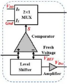
Decision Circuit
Decision circuit consists of 2x1 mux, comparator, level shifter and sense amplifier. A multiplexer (or mux) is a device that selects one of several analog or digital input signals and forwards the selected input into a single line. Low power consumption can be achieved by sense amplifiers which are main part of CMOS memory. Parasitic capacitance is much higher if memory is of high density [5]. To achieve a faster memory and less power dissipation to design sense amplifiers as, increase in number of cells per bit line which will increase
the parasitic capacitance. Minimize supply voltage lead to short amplifier reliability. Comparator is used to compare the output voltage of the NBTI (Vsensor) and the output voltage of the level shifter (Vref). A comparator is used to decide whether the SRAM cell is affected by NBTI or not. The block diagram of the decision circuit is shown in the fig 3
.
Fig 3: Decision Circuit
3.3
VB Generator Circuit
[image:2.595.62.264.496.639.2]Fig 4: VB Generator Circuit
4.
EXISTING CIRCUIT DESIGN
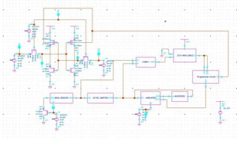
[image:3.595.54.285.425.566.2]Negative bias temperature instability (NBTI) is a major reliability issue with the scaled devices at elevated temperature. The effect of NBTI increases with the time, and it increases the threshold voltage of PMOS. In this paper, an O-ABB circuit to compensate the degradation due to NBTI aging is presented. The O-ABB is used to compensate the parameter variations and improves the SRAM circuit yield regarding read current, hold SNM, read SNM, write margin, and WLWM. The O-ABB consists of standby leakage current (Iddq) sensor circuit, decision circuit, and body bias control circuit. Circuit level simulation for SRAM cell is performed for pre- and post-stress of ten years NBTI aging. The Proposed O-ABB reduces the effect of NBTI on the stability of SRAM cell [3]. The schematic representation of existing circuit.ie, SRAM with O-ABB circuit is shown in the below fig 5.
Fig 5: Schematic of existing SRAM with O-ABB circuit
5.
PROPOSED CIRCUIT USING
MTCMOS TECHNIQUE
MTCMOS is a variation of CMOS chip technology which has transistors with multiple threshold voltages (Vth) in order
to optimize delay or power. The Vth of a MOSFET is the gate
voltage where an inversion layer forms at the interface between the insulating layer (oxide) and the substrate (body) of the transistor. Low Vth devices switch faster, and are therefore helpful on critical delay paths to minimize clock periods [13]. The consequence is that low Vth devices have considerably higher static leakage power. High Vth devices are used on non-critical paths to reduce static leakage power without incurring a delay penalty. Typical high Vth devices decrease static leakage by 10 times compared with low Vth devices.One method of creating devices with multiple threshold voltages is to apply various bias voltages (Vb) to the base or bulk terminal of the transistors. Other methods involve
adjusting the gate oxide thickness and dielectric constant (material type), or doping concentration in the channel region beneath the gate oxide [16].
A common method of fabricating multi-threshold CMOS involves just adding extra photolithography and ion-implantation step. For a given fabrication process, the Vth is adjusted by varying the concentration of doping atoms in the channel region beneath the gate oxide. In general, the concentration is adjusted by ion implantation method. For example, photolithography methods are applied to face all devices except the p-MOSFETs with photo resist [18]. Ion implantation is then finished, with ions of the chosen doping type penetrating the gate oxide in areas where no photo resist is present. The photo resist is then stripped. Photolithography methods are once more applied to cover all devices excluding the n-MOSFETs. Another implantation is then completed using a special doping type, with ions penetrating the gate oxide. The photo resist is stripped [4]. At some point during the consequent fabrication process, implanted ions are activated by annealing at an elevated temperature.
In principle, any number of threshold voltage transistors can be created. For CMOS having two threshold voltages, one extra photo masking and implantation step is necessary for each of p-MOSFET and n-MOSFET. For fabrication of normal, low, and high Vth CMOS, four additional steps are necessary relative to conventional single-Vth CMOS [14].
The most general implementation of MTCMOS for decreasing power makes use of sleep transistors. Logic is supplied by a virtual power rail. Low Vth devices are used in the logic where rapid switching speed is essential. High Vth devices connecting the power rails and virtual power rails are turned on in active mode, off in sleep mode [10]. High Vth devices are used as sleep transistors to decrease static leakage power.
The design of the power switch which turns on and off the power supply to the logic gates is necessary to low-voltage, high-speed circuit techniques such as MTCMOS. The schematic representation of proposed circuit.ie, SRAM with O-ABB circuit using MTCMOS is shown in the below fig 6.
Fig 6: Schematic of proposed SRAM with O-ABB circuit
6.
SIMUATION RESULTS AND
DISCUSSIONS
[image:3.595.315.530.494.629.2]4 Table.1 Power Comparison of Existing vs Proposed Design
Voltage in
Volts Existing Circuit
Proposed Circuit
1 5.86 1.3
0.9 2.41 535m
0.8 149m 33.1m
0.7 3.78m 840u
0.6 97.5u 21.4u
[image:4.595.319.534.253.389.2]In table 1, the power of the existing and proposed Circuit is compared. For different supply voltages and input, the power dissipation value changes. Here the power of the proposed circuit is decreased by 77.80% when compared to the existing Circuit.
Table.2 Delay Comparison of Existing vs Proposed Design
Voltage in
Volts Existing Circuit
Proposed Circuit
1 6.9p 6.97p
0.9 8p 10.2p
0.8 11.1p 15.6p
0.7 14.1p 26.7p
0.6 18.2p 44.4p
In table 2, the delay of existing and the proposed circuit is compared. For different supply voltages and input, the delay value changes.
Table.3 Power Delay Product Comparison of Existing vs Proposed Design
Voltage in
Volts Existing Circuit Proposed Circuit
1 40.434p 9.061p
0.9 19.28p 5457f
0.8 1653f 516.36f
0.7 53.298f 22.428f
0.6 1.774f 0.9501f
In table 3, the power delay product of existing and proposed circuit is compared. For different supply voltages and input, the power delay product value changes. Here the power delay product of the proposed circuit is decreased by 64% when compared to the existing circuit.
For NBTI Sensor circuit, we give the input as IDDQ (00001111) and the output as VOUT and the waveform is as shown in the fig 7.
Fig 7: Waveform of NBTI Sensor Circuit
For VB Generator circuit, we give the input as enb (10101010), clk (10101010), vdec (01010101) and the output as VB and the waveform is as shown in the fig 8.
Fig 8: Waveform of VB Generator Circuit
[image:4.595.60.275.316.444.2]For Proposed design circuit, we give the input as bl (10101010), blb (01010101), ctrl (10100000), WL (11111111), FV (11111111), SE (10010110) and the output as Q and QB and the waveform is as shown in the fig 9.
Fig 9: Waveform of Proposed design Circuit
7.
CONCLUSON AND FUTURE SCOPE
[image:4.595.314.538.442.593.2]reduced. Therefore the total power of the circuit is reduced upto 77.8% and thereby the power delay product is decreased by 64.35%. In modern day processor power dissipation plays a major role because of the miniaturization of chip design. So this MTCMOS technique can be used in future where considerable reduction of power. SRAM is used as the primary caches in powerful microprocessors. The proposed SRAM cell can be used in the area of suitable low power and hign speed applications.
8.
OBSERVATIONS FROM THE
RESULT
From the result, it is known that by various parameter such as power, delay and power delay product were calculated. Dynamic power is the power measured when circuit is in active mode. Here the power is taken into consideration for NBTI Sensor, Mux, Comparator, Level Shifter, Amplifier and Vb Generator circuit. Here the power is decreased by 15.58%, 65.74%, 27.6%, 89.12%, 97.8% and 41.2% when compared to the existing circuit. Power delay product is the parameter that is obtained by the product of power and delay value. Similarly, the power delay product of the above listed each individual circuit is decreased by 45.9%, 23.09%, 19.5%, 98.04% after applying MTCMOS technology.
9.
REFERENCES
[1] Ambika Prasad Shah , Nandakishor Yadav , Ankur Beohar, and Santosh Kumar Vishvakarma ,” On-Chip Adaptive Body Bias for Reducing the Impact of NBTI on 6T SRAM Cells”, IEEE Transactions on Semiconductor Manufacturing, Vol. 31, No. 2,242-249, May 2018.
[2] Ms.A.Gayathridevi and Mr.M.Mohan kumar ,”Power Optimization Techniques – A Study “, Asian Journal of Applied Science and Technology (AJAST) (Open Access Quarterly International Journal) Volume 2, Issue 2, Pages 909-914, April-June 2018
[3]K Gavaskar, S Priya,” Design of efficient low power stable 4-bit memory cell”, International Journal of Computer Applications (0975 – 8887) Volume 84 – No 1, December 2013
[4] Ashok Srivastava and Chuang Zhang,” An Adaptive Body-bias Generator for Low Voltage CMOS VLSI Circuits”, International Journal Of Distributed Sensor Networks, 4: 213–222, 2008.
[5] A. Calimera, M. Loghi, E. Macii, and M. Poncino, “Dynamic indexing: Leakage-aging co-optimization for caches,” IEEE Trans. Comput.-Aided Design Integr. Circuits Syst., vol. 33, no. 2, pp. 251–264, Feb. 2014.
[6]K Gavaskar, S Priya,” Design Of Efficient Low Power 9t Sram Cell”, International Journal of Engineering Research & Technology (IJERT), ISSN:2278-0181,vol.2issue 1, January-2013
[7] M. Wirnshofer, Variation-Aware Adaptive Voltage Scaling for Digital CMOS Circuits (Springer Series in Advanced Microelectronics).Heidelberg, Germany: Springer, 2013.
[8] Y. Wang, M. Enachescu, S. D. Cotofana, and L. Fang, “Variation tolerant on-chip degradation sensors for dynamic reliability management systems,” Microelectron. Rel., vol. 52, nos. 9–10, pp. 1787–1791, 2012.
[9]K Gavaskar, US Ragupathy,” Low power self-controllable voltage level and low swing logic based 11T SRAM cell for high speed CMOS circuits’, Analog Integrated
Circuits and Signal
Processing(2018)https://doi.org/1010.1007/s10470-018-1277-3.
[10] G. D. Panagopoulos and K. Roy, “A three-dimensional physical model for Vth variations considering the combined effect of NBTI and RDF,” IEEE Trans. Electron Devices, vol. 58, no. 8, pp. 2337–2346, Aug. 2011.
[11] P. Singh, E. Karl, D. Blaauw, and D. Sylvester, “Compact degradation sensors for monitoring NBTI and oxide degradation,” IEEE Trans. Very Large Scale Integr. (VLSI) Syst., vol. 20, no. 9, pp. 1645–1655, Sep. 2012.
[12] S. H. Kulkarni, D. M. Sylvester, and D. T. Blaauw, “Design-time optimization of post-silicon tuned circuits using adaptive body bias,” IEEE Trans. Comput.-Aided Design Integr. Circuits Syst., vol. 27, no. 3, pp. 481–494, Mar. 2008.
[13]K Gavaskar, US Ragupathy,” An efficient design and comparative analysis of low power memory cell structures “,2014 International Conference on Green Computing Communication and Electrical Engineering(ICGCCEE),DOI: 10.1109/ICGCCEE.2014. 6922280.
[14]J. Gregg and T. W. Chen, “Post silicon power/performance optimization in the presence of process variations using individual well-adaptive body biasing”, IEEE Trans. Very Large Scale Integr. (VLSI) Syst., vol. 15, no. 3, pp. 366–376, Mar. 2007
[15]J. W. Tschanz et al., “Adaptive body bias for reducing impacts of die-todie and within-die parameter variations on microprocessor frequency and leakage,” IEEE J. Solid-State Circuits, vol. 37, no. 11, pp. 1396–1402, Nov. 2002.
[16]M. Olivieri, G. Scotti, and A. Trifiletti, “A novel yield optimization technique for digital CMOS circuits design by means of process parameters run-time estimation and body bias active control,” IEEE Trans. Very Large Scale Integr. (VLSI) Syst., vol. 13, no. 5, pp. 630–638, May 2005.
[17]X. He, S. Al-Kadry, and A. Abdollahi, “Adaptive leakage control on body biasing for reducing power consumption in CMOS VLSI circuit,” in Proc. IEEE Int. Symp. Qual. Electron. Design (ISQED), 2009, pp. 465–470.
[18]K. K. Kim, W. Wang, and K. Choi, “On-chip aging sensor circuits for reliable nanometer MOSFET digital circuits,” IEEE Trans. Circuits Syst. II, Exp. Briefs, vol. 57, no. 10, pp. 798–802, Oct. 2010.
[19]J. Keane, T.-H. Kim, and C. H. Kim, “An on-chip NBTI sensor for measuring PMOS threshold voltage degradation,” IEEE Trans. Very Large Scale Integr. (VLSI) Syst., vol. 18, no. 6, pp. 947–956, Jun. 2010.