ISSN Online: 2153-120X ISSN Print: 2153-1196
Ab-Initio
Computations of Electronic,
Transport, and Structural Properties of
zinc-blende
Beryllium Selenide (
zb
-BeSe)
Richard Inakpenu
1, Cheick Bamba
1, Ifeanyi H. Nwigboji
2, Lashounda Franklin
1,
Yuriy Malozovsky
1, Guang-Lin Zhao
1, Diola Bagayoko
11Department of Mathematics and Physics, Southern University and A&M College, Baton Rouge, Louisiana, USA 2Computational Science Program, University of Texas at El Paso, El Paso, Texas, USA
Abstract
We report results from several ab-initio computations of electronic, transport
and bulk properties of zinc-blende beryllium selenide (zb-BeSe). Our
nonrela-tivistic calculations utilized a local density approximation (LDA) potential and the linear combination of atomic orbitals (LCAO). The key distinction of our calculations from other DFT calculations is the implementation of the Bagayoko, Zhao and Williams (BZW) method, as enhanced by Ekuma and Franklin (BZW-EF), in the LCAO formalism. Our calculated, indirect band gap is 5.46 eV, from Г to a conduction band minimum between Г and X, for a room temperature lattice constant of 5.152 Å. Available, room temperature experimental band gaps of 5.5 (direct) and 4 - 4.5 (unspecified) point to the need for additional measurements of this gap. Our calculated bulk modulus of 92.35 GPa is in excellent agreement with experiment (92.2 ± 1.8 GPa). Our predicted equilibrium lattice constant and band gap, at zero temperature, are 5.0438 Å and 5.4 eV, respectively.
Keywords
Density Functional Theory (DFT), LDA, Ab-Initio Calculations, Band Gap,
BZW-EF Method
1. Introduction and Motivations
In recent years, several studies have been carried out on the structural, electronic and transport properties of beryllium selenide (BeSe). BeSe is a member of the alkaline earth selenides. This wide band-gap semiconductor has attracted great interest for electrical and optoelectronic devices and as a promising base
materi-How to cite this paper: Inakpenu, R., Bamba, C., Nwigboji, I.H., Franklin, L., Malozovsky, Y., Zhao, G.L. and Bagayoko, D. (2017)Ab-Initio Computations of Elec-tronic, Transport, and Structural Properties of zinc-blende Beryllium Selenide (zb- BeSe). Journal of Modern Physics, 8, 552- 566.
https://doi.org/10.4236/jmp.2017.84037
Received: February 13, 2017 Accepted: March 17, 2017 Published: March 20, 2017
Copyright © 2017 by authors and Scientific Research Publishing Inc. This work is licensed under the Creative Commons Attribution International License (CC BY 4.0).
al for blue-green laser diodes and light emitting diodes [1]. This compound
crystallizes in fourfold-coordinated, cubic zinc-blende (B3) structure at ambient
temperature. A unique characteristic of this compound is the ratio of the ex-tremely small cation (Be) to a much larger anion (Se). This uniqueness accounts for the high degree of covalent bonding and is similar to the case of boron based
group III-V compounds [2]. Furthermore, the hardness, bonding energy and
stability of this compound make it a potentially good material for various tech-nological applications [3].
Few experimental studies have been performed on this compound; experi-mental difficulties include its toxic nature and its instability in air. This com-pound is difficult to handle experimentally as a single crystal or an epitaxial
layer. Yim etal. [4] prepared crystalline powder of BeSe by passing H2Se vapor
over Be metal at 1100˚C, repeatedly, for a total of 12 hours, until an X-ray powder pattern showed sharp K doublets. These authors performed measure-ments at room temperature; they estimated the band gap to be within the range of 4 - 4.5 eV and clearly stated the need for further investigations. They utilized the optical absorption measurements on cold pressed samples of BeSe powders mixed in KBr. These authors did not specify whether the band gap was direct or indirect because of shallow absorption edges and the lack of a high absorption coefficient. They stated in their work that further studies have to be done on this compound to understand the band structure. In 1999, Wilmers and his group
[5] employed spectroscopic ellipsometry in the UV/VUV region. They
investi-gated the optical properties of various samples of BexZn1-xSe by varying the stoi-chiometry of beryllium and selenium to obtain BeSe at room temperature. The BexZn1−xSe layers were grown on GaAs in a molecular-beam epitaxy chamber. The thickness of the layers ranged from 200 to 800 nm. This group analyzed the structure of the spectra in the pseudodielectric function to obtain a direct band
gap of 5.5 eV. Depending on the thickness of the actual samples of zb-BeSe, the
band gap of 5.5 eV could be a slight overestimate for the band gap of bulk
zb-BeSe; quantum confinement is known to lead to larger band gaps for thinner
films. The above two experimental reports place the band gap of zb-BeSe in the
range of 4 eV to 5.5 eV. As shown below, even the lower limit of 4 eV is unde-restimated by previous, ab-initio theoretical DFT calculations.
Several theoretical studies [6]-[21] of electronic and related properties of BeSe
have been reported. Recently, Yu etal.[6] studied the structural and electronic
properties of BeSe using the plane-wave pseudopotential method. Their
calcula-tions produced an indirect band gap of 2.73 eV. Guo and his colleagues [7]
em-ployed both GGA and LDA potentials to investigate the electronic, optical, and
structural properties of zb-BeSe. These authors utilized the plane-wave
pseudo-potential method in both calculations. They obtain an indirect band gap of 2.787 eV and 2.402 eV, respectively, with GGA and LDA potentials, from this work. The full-potential linearized augmented plane wave plus local orbitals (FP-
LAPW + lo) calculations of Allay-e-Abbas etal. [8], for the zb-BeSe, led to an
[9] respectively, obtained band gap values of 2.397 eV and 2.682 eV; they em-ployed the full-potential linearized augmented plane wave (FP-LAPW) method.
The calculated band gap value of 2.4179 eV was reported in the work of Rached etal.[10]. They utilized the full-potential linear muffin-tin orbitals (FP-
LMTO). The plane-wave pseudopotential method was employed by Srivastava et
al. [11]. They obtained a band gap of 2.43 eV. The LDA study of Khenata etal.
[12] produced a band gap of 2.475 eV. Utilizing the full-potential linearized
augmented plane wave (FP-LAPW) method, Hassan and Akbarzadeh [13]
inves-tigated the ground state properties and structural phase transition of zb-BeSe. They employed the LDA and GGA functionals to obtain two different band gaps of 2.33 eV and 2.66 eV, respectively. The full potential linearized augmented-
plane wave calculations by Berghout etal. [14], with an LDA potential, resulted
in a band gap of 2.41 eV. Another LDA study done by the same authors [12]
uti-lized the plane-wave pseudopotential method to produce a slightly higher band
gap value of 2.43 eV. Furthermore, Heciri and his group [15] performed first-
principle calculations to study the electronic structure of BeSe. In this work, the full-potential linearized augmented plane wave plus local orbital (APW + lo) method was used. They reported an indirect band gap of 2.23 eV and 2.51 eV for PW-LDA and PBE-GGA, respectively. The scalar relativistic calculation reported
by Okoye [16] is employed with full-potential linearized augmented plane wave
(FP-LAPW) approach. He obtained a band gap of 2.63 eV using the Perdew,
Burke and Ernzenhof (PBE) GGA. Table 1 below shows the GGA results are
mostly higher than those obtained with LDA potentials. The band gaps obtained from other formalisms such as Hartree Fork, Green function and screened
cou-lomb approximation (GWA) are shown in Table 1.
In addition to the previous LDA and GGA methods used by these authors [7],
they further employed the screened exchange LDA (sX-LDA) to produce a
higher band gap value of 3.455 eV. Also, Alay-e-Abbas etal.[8] used the
mod-ified Becke and Johnson (mBJ) LDA to increase the band gap to 3.53 eV.
Anoth-er pseudopotential calculation of Yadav and his group [17] found the band gap
to be 3.59 eV. They employed both GGA and GW approximation in their calcu-lations. The Engel-Vosko GGA calculations of Al-Douri et al. [9] and El Haj
Hassan etal.[13] led to a gap of 3.655 eV and 3.61 eV, respectively. Both authors
utilized the full-potential linear augmented plane wave (FP-LAPW) method. In
2000, Fleszar and Hanke [18] studied the electronic excitation in BeSe by
em-ploying the ab-initio GW approximation to produce a gap of 3.66 eV. For the
same compound, the early theoretical work performed by Stukel [19] used both
a nonrelativistic self-consistent orthogonalized plane wave (SCOPW) method and the slater's free-electron-exchange approximation to determine the energy band structure. These calculations produced an indirect band gap of 3.61 eV.
Seven years after, Sarkar and Chatterjee [20] obtained a gap of 4.37 eV from Г to
K. In their work, they applied the APW method in conjunction with an LCAO
interpolation scheme. Gonzalez-Diaz etal.[21] calculated a band gap of 2.39 eV
Table 1. Previous, calculated, indirect band gaps of zb-BeSe and room temperature experi mental values.
Computational formalism and method Potentials (DFT and Others) Eg(Г-X) eV
Norm conserving non-local pseudopotential LDA 2.39a
FP-LAPW LDA 2.475e
FP-LAPW LDA 2.33f
One electron Green’s function LDA 2.31i
Plane-wave pseudopotential LDA 2.43j
FP-LAPW LDA 2.397m
FP-LAPW LDA 2.41n
Plane-wave pseudopotential LDA 2.43n
FP-(L)APW + lo LDA 2.23b
FP-LMTO LDA 2.4179d
Plane-wave pseudopotential LDA (5.11 Å) 2.402k
Plane-wave pseudopotential sX-LDA 3.455k
FP-LAPW + lo mBJLDA 3.53c
FP-LAPW GGA 2.66f
Pseudopotential GGA 2.63h
FP-(L)APW + lo GGA 2.51b
FP-LAPW + lo GGA 2.43c
Plane-wave pseudopotential GGA (5.15 Å) 2.787k
FP-LAPW GGA (5.178 Å) 2.63l
Plane-wave pseudopotential GGA 2.737o
FP-LAPW GGA 2.682m
FP-LAPW GGA-EV 3.61f
FP-LAPW GGA-EV 3.655m
SC-OPW Slater’s Free-electron Exchange 3.61g
Pseudopotential GWA 3.59h
One-electron Green’s function GWA 3.66i
APW with LCAO Hatree-Fock self-consistent atomic potential 4.73 (Г-K)p
Experiment Spectroscopic ellipsometry 5.5 (Γ-Γ)(direct) q
Experiment Optical absorption measurement (unspecified)4 - 4.5 r
aReference [21]bReference [15]cReference [8]dReference [10]eReference [12]fReference [13]gReference [19] hReference [17]iReference [18]jReference [11]kReference [7]lReference [16]mReference [9]nReference [14] oReference [6]pReference [20]qReference [5]rReference [4].
From the theoretical results obtained with ab-initio LDA and GGA potentials,
by approximately 0.5 eV or more. The discrepancies between theoretical results
and measured band gap values of zb-BeSe are a key motivation for our work.
From the theoretical results obtained with ab-initio LDA and GGA potentials, it
is evident that the calculated band gap values were underestimated by an average of 1.5 eV or more as compared to the measured ones. While results produced by calculations using DFT-derived potentials, which are not entirely DFT poten-tials, are closer to the experimental ones, they still underestimate the latter by approximately 0.5 eV or more. The discrepancies between theoretical results and
measured band gap values of zb-BeSe are a key motivation for our work.
2. Method
In this work, the computational method used has been described in detail in
previous publications by our group [22]-[29]. We performed self-consistent
cal-culations using the Ceperley and Alder local density approximation (LDA) po-tential [30] as parameterized by Vosko, Wilk, and Nusair [31]. The computa-tional package used in this calculation is from the Ames laboratory of the US
Department of Energy (DOE), Ames, Iowa [32] [33]. We implemented the linear
combination of atomic orbitals (LCAO), using Gaussian functions in the radial parts of the orbitals. Our calculations are nonrelativistic and were first
per-formed at an experimental lattice constant of 5.152 Å (room temperature) [34].
In contrast to other calculations, we implemented the Bagayoko, Zhao, and
Wil-liams (BZW) method [22] [23] [24], as enhanced by Ekuma and Franklin (BZW-
EF) [25]. The difference between the enhanced version of our method (BZW- EF) and the previous method (BZW) is the pattern in which we increase the ba-sis set. That is the addition of orbitals. In BZW, the orbitals representing unoc-cupied energies are added to the basis set in the order of increasing, excited energies of the atomic or ionic species in the solid. The BZW-EF method add s p, d, and f orbitals, for a given principal quantum number at a given site, if ap-plicable, before adding the corresponding, spherically symmetric s orbital for that principal quantum number. This feature of the BZW-EF method rests on the realization of the primacy of the polarization of p, d, and f orbitals over the spherical symmetry of s orbitals, for the valence electrons of the material under study.
In line with the rules of the BZW-EF method, we start our calculations with a
small basis set no smaller than the minimum basis (MB), i.e., the one that is just
large enough to account for all the occupied energies in the atomic or ionic spe-cies of the material under study. We used the orbitals obtained from the
self-consistent calculations for the atomic species of Be2+ and Se2− to construct
lower than corresponding ones from Calculation I. This lowering means that the initial basis set is not complete in size, angular symmetry or radial function for the description of the ground state of the material. We then perform a third cal-culation with the basis set of Calcal-culation II plus an appropriate orbital chosen as described above. Again, we compare the occupied energies of Calculations II and
III. This process continues until three consecutive calculations, i.e., N, (N + 1)
and (N + 2), produce the same occupied energies. This fact is the criterion for
the attainment of the absolute minima of the occupied energies, i.e., the ground
state. These three calculations, upon the attainment of self-consistency, lead to the same charge density and Hamiltonian content, even though the Hamiltonian matrices have different dimensions. The first of the three calculations, N, is therefore the one providing the DFT description of the material. Its results have the full, physical content of DFT. Basis sets of Calculations (N + 1), (N + 2), and higher produce the occupied energies obtained from Calculation N, whose basis set is known as the optimal basis set. Unoccupied energies from Calculation (N + 1), (N + 2), and higher, that are different from their corresponding values from Calculation N do not belong to the spectrum of the Hamiltonian that is a unique functional of the ground state charge density, a density that did not change from its value obtained with the optimal basis set.
The above explanation for the selection of Calculation N is based on the first
DFT theorem, as first provided by Bagayoko [29]. An equally valid selection of
Calculation N is based on the Rayleigh theorem for eigenvalues. According to the Rayleigh theorem [26], successive calculations with larger basis sets that contain the optimal one generate increasing numbers of eigenvalues, by virtue of the fundamental theorem of algebra. They do not change the occupied energies. This theorem explains the lowering of some unoccupied energies by Calcula-tions (N + 1), (N + 2) and higher, after attainment of the absolute minima of the
occupied energies. This lowering is a mathematical artifact, i.e., the non-trivial
basis set and variational effect [22] [29] totally avoided by the BZW and BZW-
EF method as explained below.
The Rayleigh theorem [26] states that when the same eigenvalue equation is
solved with two basis sets containing n and (n + 1) basis functions, respectively, with the smaller basis set totally included in the larger one, then the ordered ei-genvalues (from the lowest to the highest) obtained with (n + 1) functions are lower than or equal to their corresponding values obtained with n functions. In the implementation of the BZW-EF method, we avoid the above basis set and variational effect by selecting the outputs from the calculation with the optimal
basis set, i.e., the first one to produce the absolute minima of the occupied
ener-gies. Larger basis sets, that contain the optimal basis set, produce the charge
density and Hamiltonian obtained with the optimal basis set. The changing (i.e.
lowering) of an unoccupied energy by these larger basis sets is a mathematical artifact stemming from the Rayleigh [22] [26] [29].
are at (0, 0, 0) and (1/4, 1/4, 1/4), respectively. We used a room temperature ex-perimental lattice constant of 5.152 Å for the first part of our work. We per-formed self-consistent calculations for Be2+ and Se2− to obtain the input orbitals required in generating the orbitals used in the LCGO formalism for solid state calculations. A set of even-tempered Gaussian functions were employed in con-structing the atomic orbitals of the ionic species. We used 16 even-tempered Gaussian functions with minimum and maximum exponents of 0.24 and 0.9 × 10⁵, respectively, to describe the s and p orbitals of Be2+. The s and p orbitals of Se2− were constructed using 22 even-tempered Gaussian functions, with
mini-mum and maximini-mum exponents of 0.135 and 0.24 × 10⁶, respectively. The
con-vergence for a given self-consistent calculation was attained after 60 iterations,
when the potential did not change by more than 10−5 between the last two
con-secutive iterations. The computational error made in accounting for the valence
electrons was 0.00579210 for the 28 electrons or 2.0686 × 10⁻⁴ per electron.
3. Results
Table 2 below contains orbitals employed in the successive solid state calcula-tions. This table also provides the total numbers of orbitals for the description of the valence states, along with band gaps from Г to the minima of the conduction band at high symmetry points and elsewhere.
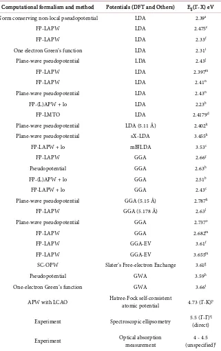
Our calculated LDA BZW-EF band structure is in Figure 1. This band
struc-ture is obtained from the basis set of Calculation II and III. It is observed that the bands from Calculation II cannot be distinguished from those from Calculation III up to 10 eV. In other words, there is a perfect superimposition of not only the occupied ones, but also for the conduction bands up to 10 eV. The calculated in-direct, band gap from Γ to a conduction band minimum between Γ and X, is 5.46 eV.
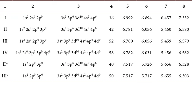
Table 2. Successive, self-consistent calculations of the BZW-EF method for zb-BeSe (Calculations I-IV) and additional, illustrative Calculations (II* & III*). The basis set of Calculation II led to the absolute minima of the occupied energies; it is the optimal basis set. Column 1: Calculation number, Column 2: Valence orbitals for Be2+, Column 3: Valence orbitals for Se2−. Column 4: Total number of valence functions, Columns 5-8: the band gaps (Eg, in eV) from Г to L, Г to Г, Г to X, and from Г to X. The optical band gap is the smallest one, in Column VII, from Г to a conduction band minimum between Г and X, as obtained with the optimal basis set.
1 2 3 4 5 6 7 8
I 1s2 2s0 2p0 3s2 3p6 3d10 4s2 4p6 36 6.992 6.894 6.457 7.332
II 1s2 2s0 2p0 3p0 3s2 3p6 3d10 4s2 4p6 42 6.781 6.056 5.460 6.580
III 1s2 2s0 2p0 3p0 3s2 3p6 3d10 4s2 4p6 4d0 52 6.780 6.056 5.459 6.579
IV 1s2 2s0 2p0 3p0 4p0 3s2 3p6 3d10 4s2 4p6 4d0 58 6.782 6.031 5.456 6.582
II* 1s2 2p0 3p0 3s2 3p6 3d10 4s2 4p6 40 7.517 5.726 5.656 6.328
[image:7.595.213.538.596.741.2]Figure 1. Electronic band structure of zb-BeSe as obtained from Calculations II (_) and III (- -), at an experimental lattice constant of 5.152 Å, using our BZW-EF method. The Fermi energy has been set to zero and its position is denoted by the horizontal, dotted lines. The calculated band gap, as obtained with the optimal basis set of Calculation II, is from Γ to a point between Γ and X. This band gap is 5.46 eV.
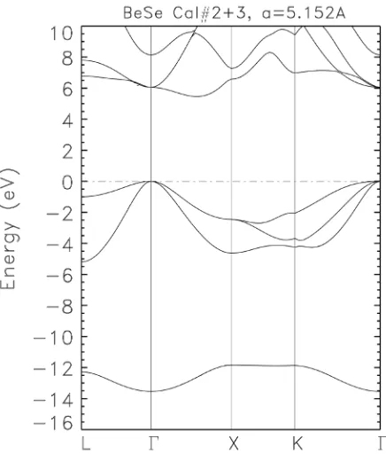
Our results for the total density of states (DOS) and partial densities of states
(pDOS) of beryllium selenide are shown in Figure 2 and Figure 3, respectively.
The total valence bandwidth is 13.59 eV. This result is close to those of Okoye
(13.8 eV) [16] and Gonzalez-Diaz (14.16 eV) [21]. The valence bands are in two
groups. The widths of the upper and lower groups are 5.25 eV and 1.81 eV, re-spectively. Our calculated width for the upper group of valence bands is close to
the finding of Rached etal. [10] of 5.42 eV. The DOS for the valence states has a
broad peak between −1 and −2.8 eV, a clear shoulder between −3 and −3.6 eV, and two sharp peaks at −4.4 and 12.0 eV. For the conduction band DOS, we found a mild shoulder at +6.4 eV and a sharp peak at +7 eV, atop a broad one from +6.4 eV to 10 eV.
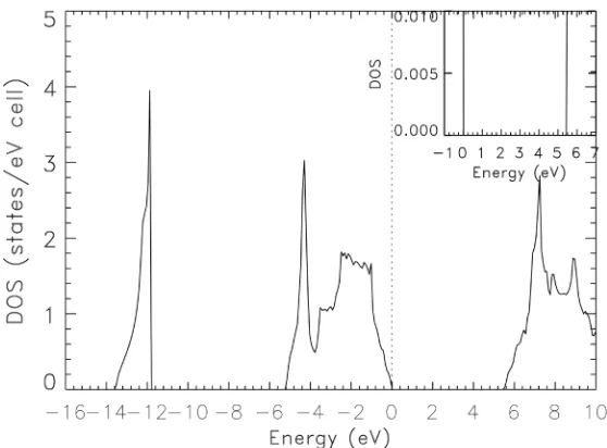
As shown in Figure 3, the partial densities of states (pDOS) describe the
con-tribution of various valence s, p, d, and states, if applicable, to the band struc-ture. The upper valence band is mainly composed of the p states from Se with slight contributions of p and s states on Be. The lowest group of valence bands consists only of the s state of Se. On the other hand, the minimum of the con-duction band, located between Γ and X, is mainly dominated by p and s states of
Be, with a minor contribution from p on Se. According to Rached etal. [10], the
Figure 2. Calculated, total density of states (DOS) for zb-BeSe, as obtained from the bands in Figure 1. The vertical, dotted line denotes the Fermi level. The value of the band gap obtained is clearly shown in the insert.
Figure 3. Calculated, partial densities of states (pDOS) for zb-BeSe, as obtained from the bands in Figure 1.
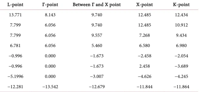
In Table 3, we list the energies of the valence and low laying conduction bands at high symmetry points in the Brillouin zone. These energies are ob-tained from the self-consistent Calculation II, using the room temperature expe-rimental lattice constant of 5.152 Å. The purpose of listing these energies is to enable detailed comparisons of our results with future experimental measure-ments, utilizing several techniques ranging from X-ray and UV spectroscopies to optical absorption.
[image:9.595.232.512.335.535.2]Table 3. Calculated, electronic energies (eV) of zb-BeSe at high symmetry points in the Brillouin zone. These energy values are obtained from the optimal basis set of Calculation II at a room temperature experimental lattice constant of 5.152 Å. The Fermi energy is set to zero in the table. The minimum points of the lowest conduction band, at the high symmetry points, are shown with bold values.
L-point Γ-point Between Γ and X point X-point K-point
13.771 8.143 9.740 12.485 12.434
7.799 6.056 9.740 12.485 10.912
7.799 6.056 9.557 7.268 9.434
6.781 6.056 5.460 6.580 6.980
−0.996 0.000 −1.673 −2.458 −2.054
−0.996 0.000 −1.673 2.458 −3.689
−5.1996 0.000 −3.007 −4.626 −4.245
−12.281 −13.542 −12.679 −11.844 −11.864
theoretical work should be in agreement with those of the measured effective masses. We calculated the electron effective mass at X in the vicinity of the
minimum of the conduction band as shown in Figure 1. From X to Г
(longitu-dinal), X to U (transverse) and X to W (transverse) directions, the results for the electron effective mass in units of m0 (free electron mass) are 1.217 m0, 0.303 m0
and 0.302 m0, respectively. Furthermore, we calculated the hole effective masses
at the top of the valence band. For heavy hole 1 along these directions, (Г-L)111,
(Г-X)100, and (Г-K)110 the effective masses are 1.309 m0, 0.572 m0 and 0.891 m0, respectively. For heavy hole 2, along the same direction, (Г-L)111, (Г-X)100, and (Г-K)110, the effective masses are 1.309 m0, 0.572 m0, and 0.637 m0, respectively. Effective masses of the light hole along (Г-L)111, (Г-X)100, and (Г-K)110, directions are 0.178 m0, 0.285 m0, and 0.235 m0, respectively. According to the calculation done by Stukel [19], the heavy hole effective masses are 1.3 m0 for Г-L(111) and 0.6
m0 for Г-X(100) while those of the light hole are 0.2 m0 for Г-L(111) and 0.3 m0 for
Г-X(100), also the electron effective mass is 1.2 m0 for Г-X(100). There are no known
experimental data available for the effective masses of zb-BeSe to compare our
results. We expect future experiments to verify our values. Our results are in
agreement with the theoretical works of Stukel [19].
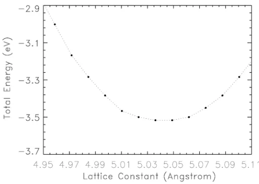
The calculated total energy versus the lattice constant is shown in Figure 4.
We utilized this curve to obtain the calculated bulk modulus which is a measure of the degree of hardness of the material. The lattice constant corresponding to the minimum value of the total energy is known as the equilibrium lattice con-stant. The value of our predicted, equilibrium lattice constant is 5.044 Å. The calculated bulk modulus is 92.3 GPa. This result is in excellent agreement with
the only experimental value known to us of 92.2 ± 1.8 GPa [32]. Other calculated
[7] [10] [11] [12] [13] [16] [17] [18] [19] LDA results produced values that are
about 1.0 GPa lower than ours. The hardness of zb-BeSe is related to its low
Figure 4. Plot of the total energy (eV) of BeSe versus the lattice constant (Å). The mini-mum value of the total energy on the curve is located at the equilibrium lattice constant of 5.044 Å.
4. Discussion
A review of the content of Table 1 leads to an obvious question. Indeed, the
pre-vious calculations utilizing ab-initio LDA or GGA potentials, unlike ours, have
uniformly underestimated the band gap of zb-BeSe. Even the calculation
utiliz-ing DFT derived ad hoc potentials mostly underestimated the band gap. The key
reasons for these underestimations are thoroughly explained by Bagayoko [29].
The first of these reasons is that the results of these calculations cannot be ex-pected to possess the full, physical content of DFT, due to the fact that they uti-lized a single basis set; such calculations lead to a stationary solution among po-tentially infinite others. The minimization resulting from self-consistent itera-tions cannot correct for any major deficiency of the selected basis set in terms of size (i.e., number of functions), angular symmetry, and radial characteristics. The successive calculations of the BZW-EF method, with the increase of the size, angular features, and radial components of the basis set, verifiably lead to the
absolute minima of the occupied energies, i.e., the ground state, as required by
the second Hohenberg-Kohn theorem.
first DFT theorem or the Rayleigh theorem for eigenvalues.
Our calculated, indirect band gap of 5.46 eV calls for further experimental in-vestigations for the following reasons. While this value is clearly in the 4 to 5.5 eV range for available experimental results, it is desirable that new experiments attempt to narrow this rather wide (1.5 eV) range. Additionally, the first experi-mental report did not specify the direct or indirect nature of the band gap. The second one found a direct band gap while our result is an indirect band gap, as qualitatively found by most of the previous, theoretical calculations. Our calcu-lated, room temperature direct gap of 6.056 eV, at Γ, is only 0.6 eV larger than our calculated, optical band gap of 5.46 eV. All measurement procedures do not
find an indirect band gap; this fact is amply illustrated in the case of TiO2 that
was considered to be a direct gap material until the work of Ekuma and Bagayo-ko [35] found an indirect one of 2.95 eV, very close to the direct one of 3.05 eV.
Santara et al. [36] confirmed the prediction of Ekuma and Bagayoko and
ex-plained how measurements with non-polarized light could not find this indirect band gap, but they led to the slightly larger direct gap for TiO2.
5. Conclusion
In conclusion, we have performed ab-initio, self-consistent calculations of
elec-tronic energy bands, total density of states (DOS), partial densities of states
(pDOS), effective masses and bulk modulus of zb-BeSe. The distinctive feature
of our calculations as compared to previous ab-initio and empirical calculations
is the implementation of the Bagayoko, Zhao, and Williams (BZW) method, as enhanced by Ekuma and Franklin (BZW-EF). Our calculated, indirect band gap is 5.46 eV, from Г to a conduction band minimum between Г and X, for a room temperature lattice constant of 5.152 Å. Our bulk modulus is in excellent agree-ment with experiagree-ment within the experiagree-mental uncertainties. Our results for the band gap, DOS, pDOS, effective masses and bulk modulus, along with similar
ones from this group [22] [23] [24] [25] [26], strongly suggest that LDA BZW-
EF calculations have the capability to accurately describe and predict electronic and related properties of semi-conductors. Based on this capability, our calcula-tions are expected to inform and to guide the design and fabrication of semi-conductor-based devices. Our results and the limited, available experimental ones strongly suggest the need for further measurements of electronic properties of zb-BeSe, including its band gap.
Acknowledgements
This work was funded in part by the US Department of Energy (DOE), National Nuclear Security Administration (NNSA) (Award No.DE-NA0002630), the Na-tional Science Foundation (NSF) (Award No, 1503226), LaSPACE, and LONI- SUBR.
References
Gerhardt, T. and Moller, M. (1996) Molecular-Beam Epitaxy of Beryllium Chalco-genides Based Thin Films and Quantum-Well Structures. JournalofApplied Phys-ics, 80, 792-796. https://doi.org/10.1063/1.362888
[2] Luo, H., Ghandehari, K., Greene, R., Ruoff, A., Trail, S. and DiSalvo, F. (1995) Phase Transformation of BeSe and BeTe to the NiAs Structure at High Pressure. Physical ReviewB, 52, 7058-7064. https://doi.org/10.1103/PhysRevB.52.7058
[3] Bouhafs, B., Aourag, H. and Certier, M. (2000) Trends in Band-Gap Pressure Coefficients in Boron Compounds BP, BAs, BSb. Journal of Physics Condensed Matter, 12, 5655-5668. https://doi.org/10.1088/0953-8984/12/26/312
[4] Yim, W.M., Dismakes, J.B., Stofko, E.J. and Paff, R.J. (1972) Synthesis and Some Properties of BeTe, BeSe and BeS. JournalofPhysicsandChemistryofSolids, 33, 501-505.
[5] Wilmers, K., Wethkamp, T., Essar, N., Cobet, C., Richter, F., Wagner, V., Lugauer, H., Fischer, F., Gerhard, T. and Keim, M. (1999) Ellipsometric Studies of BexZn1-xSe between 3 eV and 25 eV. PhysicalReviewB, 59, 10071-10075.
https://doi.org/10.1103/PhysRevB.59.10071
[6] Yu, Y., Liu, D., Chen, J., Ji, J. and Long, J. (2014) First-Principles Investigations on Structural, Electronic and Elastic Properties of BeSe under High Pressure. Solid StateSciences, 28, 35-40.
[7] Guo, L., Hu, G., Zhang, S., Feng, W. and Zhang, Z. (2013) Structural, Elastic, Elec-tronic and Optical Properties of Beryllium Chalconides BeX (X=S, Se, Te) with
zinc-blende Structure. JournalofAlloysandCompounds, 561, 16-22.
[8] Alay-e-Abbas, S.M., Wong, K.M., Noor, N.A., Shaukat, A. and Lei, Y. (2012) An Ab-Initio Study of the Structural, Electronic and Magnetic Properties of Half-Metallic Ferromagnetism in Cr-Doped BeSe and BeTe. SolidStateScience, 14, 1525-1535.
[9] Al-Douri, Y., Baaziz, H., Charifi, Z. and Reshak, A.H. (2012) Density Functional Study of Optical Properties of Beryllium Chalcogenides Compounds in Nickel Ar-senide B8 Structure. PhysicaB, 407, 286-296.
[10] Rached, D., Rabah, M., Benkhettou, N., Khenata, R., Soudini, B., Al-Douri, Y. and Baltache, H. (2006) First-Principle Study of Structural, Electronic and Elastic Prop-erties of Beryllium Chalcogenides BeS, BeSe and BeTe. Computational Materials Science, 37, 292-299.
[11] Srivastava, G.P., Tutuncu, H.M. and Gunham, N. (2004) First-Principles Studies of Structural, Electronic, and Dynamical Properties of Be Chalcogenides. Physical Re-viewB, 70, Article ID: 85206. https://doi.org/10.1103/PhysRevB.70.085206
[12] Khenata, R., Bouhemadou, A., Hichour, M., Baltache, H., Rached, D. and Rerat, M. (2006) Elastic and Optical Properties of BeS, BeSe and BeTe under Pressure. Sol-id-StateElectronics, 50, 1382-1388.
[13] Hassan, F.E. and Akbarzadeh, H. (2006) Ground State Properties and Structural Phase Transition of Beryllium Chalcogenides. ComputationalMaterialsScience, 35, 423-431.
[14] Berghout, A., Zaoui, A. and Hugel, J. (2006) Fundamental State Quantities and High-Pressure Phase Transition in Beryllium Chalcogenides. Journal of Physics CondensedMatter, 18, 10365-10375. https://doi.org/10.1088/0953-8984/18/46/005 [15] Heciri, D., Beldi, L., Drablia, S., Meradji, H., Derradji, N.E., Belkhir, H. and
[16] Okoye, C. (2004) Structural, Electronic, and Optical Properties of Beryllium Mo-nochalcogenides. EuropeanPhysicalJournalB, 39, 5-17.
https://doi.org/10.1140/epjb/e2004-00164-3
[17] Yadav, P.S., Yadav, R.K., Agrawal, S. and Agrawal, B.K. (2007) Ab-Initio Study of Electronic and Optical Properties of Be-Chalcogenides in GW Approximation. Phy-sicaE, 36, 79-85.
[18] Fleszar, A. and Hanke, W. (2000) Electronic Excitations in Beryllium Chalcogenides from the Ab-Initio GW approach. PhysicalReviewB, 62, 2466.
https://doi.org/10.1103/PhysRevB.62.2466
[19] Stukel, D.J. (1970) Energy-Band Structure of BeS, BeSe and BeTe. PhysicalReview B, 2, 1852. https://doi.org/10.1103/PhysRevB.2.1852
[20] Sarkar, R.L. and Chatterjee, S. (1977) Electronic Energy of BeSe and BeTe. Journal ofPhysicsC, 10, 57. https://doi.org/10.1088/0022-3719/10/1/011
[21] Gonzales-Diaz, M., Rodriguez-Hernandez, P. and Munoz, A. (1997) Elastic Constants and Electronic Structure of Beryllium Chalcogenides BeS, BeSe, and BeTe from First-Principles Calculations. PhysicalReviewB, 55, Article ID: 14043. https://doi.org/10.1103/PhysRevB.55.14043
[22] Bagayoko, D., Zhao, G.L., Fan, J.D. and Wang, J.T. (1998) Ab-Initio Calculations of the Electronic Structure and Optical Properties of Ferroelectric Tetragonal BaTiO3.
JournalofPhysicsCondensedMatter, 10, 5645. https://doi.org/10.1088/0953-8984/10/25/014
[23] Bagayoko, D., Franklin, L. and Zhao, G.L. (2004) Predictions of Electronic, Struc-tural, and Elastic Properties of Cubic InN. Journal of Applied Physics, 96, 4297-4301. https://doi.org/10.1063/1.1790064
[24] Bagayoko, D. and Franklin, L. (2005) Density Functional Theory Band Gap of Wurtzite InN. JournalofAppliedPhysics, 97, Article ID: 123708.
https://doi.org/10.1063/1.1939069
[25] Ekuma, C.E., Bagayoko, D., Jarrell, M. and Moreno, J. (2013) Electronic, Structural, and Elastic Properties of Metal Nitrides XN (X = Sc, Y): A First Principle Study. AIP Advances, 2, Article ID: 032163. https://doi.org/10.1063/1.4751260
[26] Bagayoko, D. (1983) Contraction of Gaussian Basis Sets and the Total Energy of FCC Copper. International JournalofQuantumChemistry, 24, 527-535.
https://doi.org/10.1002/qua.560240857
[27] Franklin, L., Ekuma, C.E., Zhao, G.L. and Bagayoko, D. (2013) Density Functional Theory Description of Electronic Properties of Wurtzite Zinc Oxide. Journal of PhysicsandChemistryofSolids, 74, 729-736.
[28] Ekuma, C.E., Jarrell, M., Moreno, J. and Bagayoko, D. (2013) Re-Examining the Electronic Structure of Germanium: A First Study Principle Study. PhysicsLetterA, 377, 2172.
[29] Bagayoko, D. (2014) Understanding Density Functional Theory (DFT) and Com-pleting It in Practice. AIPAdvances, 4, Article ID: 127104.
https://doi.org/10.1063/1.4903408
[30] Ceperly, D.M. and Alder, B.J. (1980) Ground State of the Electron Gas by a Stochas-tic Method. PhysicalReviewLetter, 45, 566-569.
https://doi.org/10.1103/PhysRevLett.45.566
[31] Vosko, S.H., Wilk, L. and Nusair, M. (1980) Ground State of the Electron Gas by a Stoichastic Method. CanadianJournalofPhysics, 58, 1200-1211.
https://doi.org/10.1139/p80-159
a Ti (0001) Film. PhysicalReviewB, 20, 1433-1443. https://doi.org/10.1103/PhysRevB.20.1433
[33] Harmon, B.N., Weber, W. and Hamann, D.R. (1982) Total Energy Calculations for Si with First Principles Linear Combination of Atomic Orbitals Method. Physical ReviewB, 25, 1109-1115. https://doi.org/10.1103/PhysRevB.25.1109
[34] Gall R, (1997) Diplomarbeit. Wurzburg University, Wurzburg.
[35] Ekuma C.E. and Bagayoko, D. (2011) Ab-Initio Electronic and Structural Properties of Rutile Titanium Dioxide. JapaneseJournal of AppliedPhysics, 50, Article ID: 101103. https://doi.org/10.7567/JJAP.50.101103
[36] Santara, B., Giri P.K., Imakita, K. and Fujii, M. (2014) Microscopic Origin of Lattice Contraction and Expansion in Undoped Rutile TiO2 Nanostructures. Journal of
PhysicsD: AppliedPhysics, 47, Article ID: 215302. https://doi.org/10.1088/0022-3727/47/21/215302
Submit or recommend next manuscript to SCIRP and we will provide best service for you:
Accepting pre-submission inquiries through Email, Facebook, LinkedIn, Twitter, etc. A wide selection of journals (inclusive of 9 subjects, more than 200 journals)
Providing 24-hour high-quality service User-friendly online submission system Fair and swift peer-review system
Efficient typesetting and proofreading procedure
Display of the result of downloads and visits, as well as the number of cited articles Maximum dissemination of your research work
Submit your manuscript at: http://papersubmission.scirp.org/