ISSN Online: 2327-5227 ISSN Print: 2327-5219
DOI: 10.4236/jcc.2019.76003 Jun. 30, 2019 15 Journal of Computer and Communications
Broad Band Microstrip Patch Antenna Based on
Foam-Filled and One Open Slot on Backward of
Radiating Layer
Ali Esseid Almuzwghi, Lail Brian
Department of Computer Engineering and Science, Florida Institute of Technology, Melbourne, FL, USA
Abstract
A broadband microstrip patch antenna, loaded E-U-shaped open slot on backward of radiating layer is proposed and experimentally investigated. The antenna employs a foam-filled dielectric substrate, whose dielectric constant is within the lower end of the range. The proposed antenna has been designed for electromagnetic analysis including the impedance bandwidth, reflection coefficient, radiation pattern, and antenna gain. The open slot is loaded on the back radiated layer, which is perpendicular to the radiating edge of the oblong microstrip patch component, where the symmetric line feed is se-lected. This new technique used to increase the bandwidth and the gain of antenna through increasing current path by slot location, width and length on backward of radiating Layer. The main structure in this research was a single microstrip patch antenna planar with three layers operating at two resonant frequencies 4.440 GHz and 5.833 GHz. All the simulated results are con-firmed by two packages of electromagnetism simulation. An impedance bandwidth (S11 ≤ −10 dB) up to about 41.03% and 30.61% is achieved by in-dividually optimizing its parameters. The antenna exhibits nearly stable ra-diation pattern with a maximum gains of 8.789 dBi and 9.966 dBi, which is suitable for Wi-Fi Band, satellite communications, and wireless presented. Whereas the results before this design that we have a proof of publication are 36.17% and 28.43%.
Keywords
Broad Band, Foam, One Open Slot, Three Layers, Two Packages, Electromagnetism Simulation
1. Introduction
With a booming period and desire in modern wireless communication applica-tions, microstrip patch antennas have attracted much interest due to their com-How to cite this paper: Almuzwghi, A.E.
and Brian, L. (2019) Broad Band Microstrip Patch Antenna Based on Foam-Filled and One Open Slot on Backward of Radiating Layer. Journal of Computer and Commu-nications, 7, 15-28.
https://doi.org/10.4236/jcc.2019.76003
Received: April 14, 2019 Accepted: June 27, 2019 Published: June 30, 2019
Copyright © 2019 by author(s) and Scientific Research Publishing Inc. This work is licensed under the Creative Commons Attribution International License (CC BY 4.0).
DOI: 10.4236/jcc.2019.76003 16 Journal of Computer and Communications patibility with printed circuits without problems, light weight, profile, and ease of fabrication [1][2][3][4]. A major challenge of microstrip patch antenna de-sign comprises its commercialization that requires wide impedance bandwidth, high efficiency and high gain along with taking care at a low price in a single de-sign. For over a period two decades, investigators and scientists have developed several methods to increase the impedance bandwidth, high efficiency and high gain of patch antenna. One of that methods, the impedance bandwidth of the microstrip patch antenna, increases with a decrease in the relative permittivity dielectric constant (Єr) [5][6][7] or with an increase in the layer thickness (h) [7][8][9] [10]. However, there is an experiential limit on increasing the layer thickness (h), while if increased beyond 0.1 wavelength (λ0), surface-wave propagation comes out, resulting in degradation in antenna performance. The bandwidth larger than 25% is accomplished utilizing gap-coupled coplanar mi-crostrip resonators [10]. Another conventional broad-banding technique in-cludes the use and inserting relatively thick air-gap [11] or foam-gap substrate [12], and in addition, organizing a two or more patches antenna on different layers of the dielectric substrates in one pile (stacked) [13] to achieve wide bandwidth.
In recent years, many designs have been reported to achieve wideband patch antenna for modern wireless communication devices. That includes use of vari-ous formed slot, slit and patch like U-shape slot antenna [14][15][16][17][18], wide band E-shape patch antenna [19] [20]. However, their realizable band-widths of these designs are below 30%. As example on that, covered dielectric layer which is separated from feed patch by air as another dielectric [21], an im-pedance bandwidth of 220 MHz, is achieved and gain is found as 13.4 dBi. The structure in this design is 2 by 2 microstrip patch planar array antenna using air substrate with (Єr = 1) at frequency 5.8 GHz [22]. The results show that the gain increases up to 14.63 dBi if using air substrate compared to FR-4 substrate (9.04 dBi). In another novel antenna structure which contains five substrate layers [23], the eight-element antenna array with feeding network achieved frequency band from 5.28 to 6.05 GHz 15.4% and antenna gain of 16.24 dBi. Most of the reported papers in the literature are more complexes, high-cost, and have achieved a maximum bandwidth of 30% with gain below 16.24 dBi. The pro-posed design is low-cost and very simple with a single patch. It has achieved gain of 8.789 dBi and 9.966 dBi at a resonant frequency of 4.450 GHz and 5.833 GHz with directivity of 9.782 dBi and 10.262 dBi and a bandwidth of 41.03% and 30.61% respectively.
DOI: 10.4236/jcc.2019.76003 17 Journal of Computer and Communications
2. Antenna Design
The one that is most recommendable for good reception apparatus execution are thick substrates, whose dielectric steady is in the lower value enclosed to 1 since they give better they provide better efficiency, produce high gain, and increase wide band. In this paper the impedance band and the gain proposed has been improved using foam substrate where dielectric constant Єr = 1.03 has thickness 3.2 mm.
The first design, the foam substrate is inserted between the radiation layer and ground plane. The radiation layer used the Rogers_RT_Duroid5881 substrate with thickness 1.6 mm and permittivity (Єr) = 2.17 when the tangent loss is 0.0009 at top layer, whereas, the ground layer used the Rogers_RT_Duroid5870 substrate with thickness 1.6 mm and permittivity (Єr) = 2.33 when the tangent loss is 0.0012 at the bottom layer as shown in Figure 1.
[image:3.595.213.534.450.709.2] [image:3.595.215.530.451.552.2]The second design inserted driven layer (printed figure) between the radiating layer and foam gap. The driven layer is E-shaped or U-shaped. The dimensions of the patch antenna and driven layer are shown in Figure 2 and Table 1. This technique making multilayer microstrip antenna has ability obtained enhanced bandwidth, enhanced gain of antenna, and better efficiency. In addition, the feed line used to feed the antenna. Microstrip line feed structure is more suitable if compared to Coaxial feed, due to no difficulty of fabrication, compatibility with printed circuits without problems and lower costs. Finally, the idea of this paper is to present the simulation results of our study of the antenna parameters under conditions, by means of an adjustable the distance between the top printed fig-ure and the end edge of the point feed (D-L) and printed-figfig-ure style.
Figure 1. Design of the proposed antenna.
[image:3.595.213.535.588.703.2]DOI: 10.4236/jcc.2019.76003 18 Journal of Computer and Communications
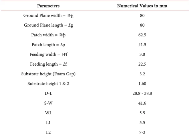
Table 1. Optimized values of proposed patch antenna parameters.
Parameters Numerical Values in mm
Ground Plane width = Wg 80
Ground Plane length = Lg 80
Patch width =Wp 62.5
Patch length = Lp 41.5
Feeding width = Wf 3.0
Feeding length = Lf 22.5
Substrate height (Foam Gap) 3.2
Substrate height 1 & 2 1.60
D-L 28.8 - 38.8
S-W 41.6
W1 5.5
L1 5.5
L2 7-3
Optimized Antenna Design
The sizes of the metallic antenna were slightly changed in order to enhance the antenna performance parameters. It is optimized from 28.8 mm to 38.2 mm in 1.0 mm increments, where the other parameters are constant. Finally, the total area of the ground plane is 80 mm × 80 mm and the total area of the patch an-tenna is 62.5 mm × 41.5 mm.
3. Results and Discussion
3.1. Antenna Design without Printed Figure and Foam Gap
Microwave office (AWR) version 2018 and Advance Design System (ADS) ver-sion 2016 were used, whereas MATLAB used to compare the simulation results. All the results are displayed graphically and numerically, where the simulators have been utilized to acquire these outcomes. The main purpose of different al-gorithms simulation are to support objective decision making by means of re-sults analysis, to enable design to safely plan their operations, and to compare favorably with present different algorithms. The results simulated a successfully to operate at specified frequencies are perfect agreement between different algo-rithms simulation.
3.1.1. Simulation Results of Patch without Foam Gap and Driven Layer
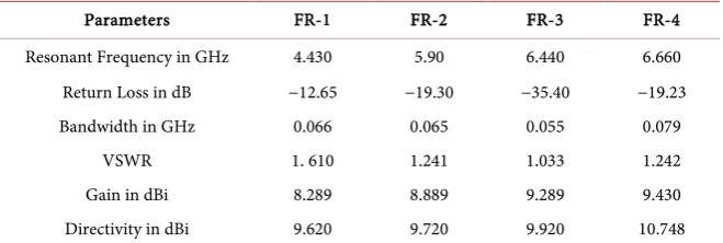
DOI: 10.4236/jcc.2019.76003 19 Journal of Computer and Communications 6.438 GHz, and (RL-4)-15.57 dB at 6.662 GHz was obtained by ADS. The corre-sponding impedance bandwidths are (BW-1) 0.066 GHz, (BW-2) 0.065 GHz, (BW-3) 0.055 GHz, and (BW-4) 0.079 GHz. That is clear sure, the reflection co-efficients and the resonant frequencies show better agreement between two software simulations. Both results prove that the antenna has good performance both. The small discrepancies between two simulated results could be attributed, because the two software’s have the different logarithmic (Table 2).
3.1.2. Simulation Results of Patch with Foam Gap and without Driven Layer
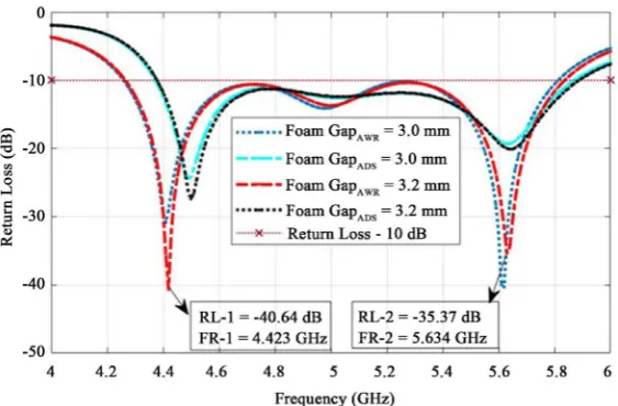
[image:5.595.234.515.286.472.2]Simulated results of microstrip patch antenna show the effect the thickness of foam gap in Figure 4, which have −40.46 dB and −35.37 dB return losses with increased bandwidth up to 1.589 GHz at 4.423 GHz and 5.634 GHz frequencies, which are 35.91 and 28.23 percent more than single patch antenna without gap.
Figure 3. Return loss obtained by AWR and ADS of antenna without Gap and driven
layer.
[image:5.595.233.515.519.704.2]DOI: 10.4236/jcc.2019.76003 20 Journal of Computer and Communications
Table 2. Summary of simulated results of design an antenna without gap and slot.
Parameters FR-1 FR-2 FR-3 FR-4
Resonant Frequency in GHz 4.430 5.90 6.440 6.660 Return Loss in dB −12.65 −19.30 −35.40 −19.23
Bandwidth in GHz 0.066 0.065 0.055 0.079
VSWR 1. 610 1.241 1.033 1.242
Gain in dBi 8.289 8.889 9.289 9.430
Directivity in dBi 9.620 9.720 9.920 10.748
3.1.3. Simulation Results of Patch with Foam Gap and Driven Layer
In order to fully understand the influence of the space between the top of printed figure and the edge of feed the patch (D-L) parameter, the parametric investiga-tion was carried out by varying this parameter, while holding still existing pa-rameters values as Section 2. This simulation was conducted using two different designs.
3.2. Antenna Design with Printed Figure
3.2.1. The Effect of Print Figure E Shape on Power Reflection Coefficient and Resonance Frequency
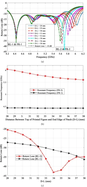
Figure 5(a) shows the parametric effect (D-L) on the reflection coefficient (S11
≤ −10 dB), and resonant frequencies when (D-L) parameter are varied.
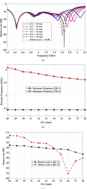
The following section in Figure 5(b) shows the effect of a variable parameter (D-L), with the increase in the (D-L), the resonant frequency (FR-2) curve shifts towards lower resonant frequencies, while there is no significant change in the resonant frequency (FR-1).
AS the D-L smoothly increased, there are more amount to the fringing effects occurred, this leads to a better return loss (RL-1), whereas return loss (RL-2) has a maximum amount at D-L is equal 34mm, after that, it turn into inverse direc-tion as shown in Figure 5(c).
3.2.2. Bandwidth by Taking the (D-L) as a Parameter for Patch Antenna
The distance (D-L), is varying from 28.0 mm to 29.0 mm, there is very little variation in the absolute value of the bandwidth (BW-1) and the bandwidth (BW-2). The bandwidth (BW-1) and the bandwidth (BW-2) have a rapid in-crease to the maximum value where the distance (D-L) has an inin-crease from 29.0 mm to 30.0 mm, whereas the distance 30.0 mm to 38.0 mm all bandwidths are a slowly decrease as shown the result in Figure 6. A significant bandwidth is ob-served at distance of the printed figure beyond at 30.0 mm, it is appreciable ex-tent. In these points of observation, the bandwidths are close to 1.821 GHz or 41.03% and 30.61%.
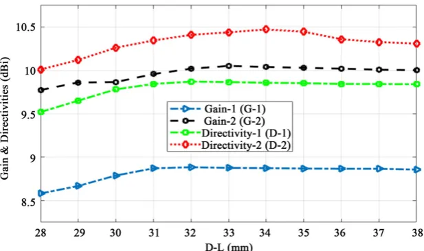
3.2.3. Gains and Directivities by Taking the (D-L) as a Parameter for Patch Antenna
Figure 7 shows directivities and gains Vs distance (D-L). All directivities are
DOI: 10.4236/jcc.2019.76003 21 Journal of Computer and Communications (a)
(b)
[image:7.595.233.519.66.682.2](c)
Figure 5. (a) Power reflection coefficient (S11) and resonance frequency different values
DOI: 10.4236/jcc.2019.76003 22 Journal of Computer and Communications
[image:8.595.220.529.302.485.2]Figure 6. Bandwidth for figure E shape at different values of (D-L).
Figure 7. Gains and directivities for different values of (D-L).
38.0 mm directivities are a slowly decrease. However, gains are slowly increasing from 28.0 mm to 34.0 mm, whereas the distance at 34.0 mm to 38.0 mm gains are a slowly decrease.
3.3. Design Antenna with Printed Figure U-Shaped
The Effect of Print Figure U Shape on Power Reflection Coefficient and Resonance Frequency
The simulated plot of varied reflections coefficient (S11 < −10 dB) and resonant frequencies that obtained by effect various lengths D-L from 28 mm until 38mm is shown in Figure 8(a).
Figure 8(b) shows the general effect of the variable parameter (D-L), with the
DOI: 10.4236/jcc.2019.76003 23 Journal of Computer and Communications (a)
(b)
[image:9.595.232.516.63.675.2](c)
Figure 8. (a) Power reflection coefficient (S11) and resonance frequency different values
DOI: 10.4236/jcc.2019.76003 24 Journal of Computer and Communications AS the D-L move towards a higher increased there more amount to the fring-ing effects occurred, and this leads to a better return loss (RL-1), whereas return loss (RL-2) has a maximum amount at D-L is equal 36mm. After that, it turns into inverse direction as shown in Figure 8(c).
3.4. The Dissimilarity between the Figures E and U
3.4.1. The Dissimilarity of Resonance Frequencies
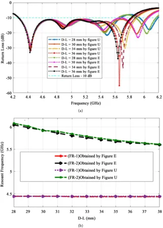
Two resonant frequencies obtained from the conventional patch antenna with the figures E and U. The results very similar of the simulation of two different designs as shown in Figure 9(a) and Figure 9(b) were obtained.
(a)
[image:10.595.213.536.232.682.2](b)
Figure 9. (a) Dissimilarity between the figures of E-shape and U-shape of reflection
DOI: 10.4236/jcc.2019.76003 25 Journal of Computer and Communications 3.4.2. The Dissimilarity of Return Losses
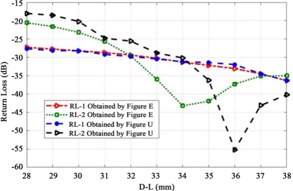
The results of return loss (RL-1) very similar of the simulation of two different designs as shown in Figure 9(a) and Figure 10 were obtained, whereas, return loss (RL-2) dissimilar it's irregular, It is a balanced values with activities effi-ciency by a specified way of the current path that pass through the patch an-tenna.
3.4.3. The Dissimilarity of Bandwidths
Two bandwidths obtained from the conventional patch antenna with the figures E and U. The results very similar of the simulation of two different designs as shown in Figure 11 were obtained.
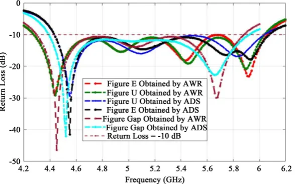
[image:11.595.231.518.303.490.2]The simulated of bandwidths are 41.03% and 30.61% covering the (4.270 - 6.091 GHz) obtained by figure-E, whereas the simulated bandwidths are 40.18% and 30.12% covering the (4.277 - 6.061 GHz) obtained by figure-U, as shown in
[image:11.595.230.517.523.703.2]Figure 12, Figure 13 and Table 3.
Figure 10. Dissimilarity between the figures of E-shape and U-shape of return losses.
DOI: 10.4236/jcc.2019.76003 26 Journal of Computer and Communications
Figure 12. Variation reflection coefficient and resonant Frequency under the Foam Gap,
[image:12.595.225.524.304.512.2]E-Figure, and U-Figure influences.
Figure 13. Variation VSWR and resonant frequency under the Foam Gap, E-Figure, and
U-Figure influences.
Table 3. Summary of simulated results of final design an antenna.
Parameters Figure E Figure U Foam
Resonant Frequencies in GHz 4.442 - 5.833 4.440 - 5.920 4.425 - 5.632 Return Loss in dB 28.47 - 21.65 28.21 - 23.06 40.64 - 35.37 Bandwidth in % 41.03 - 30.61 40.18 - 30.10 36.17 - 28.43
Bandwidth in GHz 1.821 1.784 1.628
[image:12.595.210.540.577.725.2]DOI: 10.4236/jcc.2019.76003 27 Journal of Computer and Communications
4. Conclusion
In this paper, the antenna design has been simulated successfully to operate at specified frequencies through specified new technique simulated by different al-gorithms with perfect agreement of results, whereas, the specified frequencies are 4.440GHz and 5. 5.833 GHz. The simulation results demonstrate clearly and definitely that new technique can be used to optimize bandwidth and gain for specified antenna. The bandwidths have been obtained 41.03% and 30.61% for specified frequencies respectively to operate in wireless communications appli-cation at Wi-Fi band. The designed antenna has power reflection coefficient (S11) of −28.62 dB and −23.41 dB for specified frequencies respectively. The de-signed broad band antenna has a VSWR value of 1.086 and 1.248. The value of the directivity is 9.782 dBi and 10.262 dBi and the gain magnitude is 8.789 dBi and 9.966 dBi.
Conflicts of Interest
The authors declare no conflicts of interest regarding the publication of this pa-per.
References
[1] Balanis, C.A. (1997) Antenna Theory, Analysis and Design. John Wiley & Sons, New York.
[2] Xiong, J., Ying, Z. and He, S. (2008) A Broadband E-Shaped Patch Antenna of Compact Size and Low Profile. IEEE Antennas and Propagation Society Interna-tional Symposium, San Diego, 5-11 July 2008, 1-4.
[3] Ali, J.K. (2011) A New Dual Band E-Shaped Slot Antenna Design for Wireless Ap-plications. Progress in Electromagnetics Research Symposium, Suzhou, 12-16 Sep-tember 2011, 12-16.
[4] Kumar, G. and Ray, K.P. (2003) Broadband Microstrip Antennas. Artech House, Norwood, MA.
[5] Chen, W. and Lee, K.F. (1993) Input Impedance of Coaxially Fed Rectangular Mi-crostrip Antenna on Electrically Thick Substrate. Microwave and Optical Technol-ogy Letters, 6, 387-390.https://doi.org/10.1002/mop.4650060616
[6] Bhattacharayya, A.K. (1990) Characteristics of Space and Surface-Waves in a Multi-layered Structure. IEEE Transactions on Antennas and Propagation, 38, 1231-1238. https://doi.org/10.1109/8.56959
[7] Almuzwghi, A.E. and Brian, L. (2019) Broad Band Microstrip Patch Antenna Using Foam Gap Substrate for Wi-Fi Band. International Journal of Engineering Research and Applications, 9, 48-52.
[8] Radavaram, S. and Pour, M. (2019) Wideband Radiation Reconfigurable Microstrip Patch Antenna Loaded with Two Inverted U-Slots. IEEE Transactions on Antennas and Propagation, 67, 1501-1508. https://doi.org/10.1109/TAP.2018.2885433 [9] Kara, M. (1998) Design Considerations for Rectangular Microstrip Antenna
Ele-ments with Various Substrate Thicknesses. Microwave and Optical Technology Letters,19, 111-121.
DOI: 10.4236/jcc.2019.76003 28 Journal of Computer and Communications [10] Tong, K.F., Luk, K.M., Lee, K.F. and Lee, R.Q. (1993) A Broad-Band U-Slot Rec-tangular Patch Antenna on a Microwave Substrate. IEEE Transactions on Antennas and Propagation, 48, 954-960. https://doi.org/10.1109/8.865229
[11] Ayoub, A.F.A. (2003) Analysis of Rectangular Microstrip Antennas with Air Sub-strates. Journal of Electromagnetic Waves and Applications, 17, 1755-1756. https://doi.org/10.1163/156939303322760335
[12] Luk, K.M., Mak, C.L., Chow, Y.L. and Lee, K.F. (1998) Broadband Microstrip Patch Antenna. Electronics Letters, 34, 1442-1443.https://doi.org/10.1049/el:19981009 [13] Anguera, J., Puente, C., Borja, C., Delbene, N. and Soler, J. (2003) Dual Frequency
Broadband Stacked Microstrip Patch Antenna. IEEE Antennas and Wireless Prop-agation Letters, 2, 36-39.https://doi.org/10.1109/LAWP.2003.811325
[14] Huynh, T. and Lee, K.F. (1995) Single-Layer Single-Patch Wideband Microstrip Antenna. Electronics Letters, 31, 1310-1312.https://doi.org/10.1049/el:19950950 [15] Tong, K.F., Luk, K.M., Lee, K.F. and Lee, R.Q. (2000) A Broad-Band U-Slot
Rec-tangular Patch Antenna on a Microwave Substrate. IEEE Transactions on Antennas and Propagation, 48, 954-960. https://doi.org/10.1109/8.865229
[16] Lee, K.F., Luk, K.M., Tong, K.F., Yung, Y.L. and Huynh, T. (1996) Experimental Study of a Two-Element Array of U-Slot Patches. Electronics Letters, 32, 418-420. https://doi.org/10.1049/el:19960290
[17] Lee, K.F., Luk, K.M., Tong, K.F., Shum, S.M., Huynh, T. and Lee, R.Q. (1997) Ex-perimental and Simulation Studies of Coaxially Fed U-Slot Rectangular Patch An-tenna. IEE Proceedings—Microwaves, Antennas and Propagation, 144, 354. https://doi.org/10.1049/ip-map:19971334
[18] Tong, K.F. and Wong, T.P. (2007) Circularly Polarized U-Slot Antenna. IEEE Transactions on Antennas and Propagation, 55, 2382-2385.
https://doi.org/10.1109/TAP.2007.901930
[19] Kumar, G. and Ray, K.P. (2003) Broadband Microstrip Antennas. Artech House, Norwood, MA.
[20] Deshmukh, A.A. and Kumar, G. (2005) Compact Broadband E-Shaped Microstrip Antennas. Electronics Letters, 4, 989-990.https://doi.org/10.1049/el:20051789 [21] Kharade, A.R. and Patil, V.P. (2012) Enhancement of Gain of Rectangular Micro
Strip Antenna Using Multilayer Multi Dielectric Structure. IOSR Journal of Elec-tronics and Communication Engineering, 2, 35-40.
https://doi.org/10.9790/2834-0263540
[22] Ali, M.T., Jaafar, H., Subahir, S. and Yusof, A.L. (2012) Gain Enhancement of Air Substrates at 5.8 GHz for Microstrip Antenna Array. 2012 Asia-Pacific Symposium on Electromagnetic Compatibility, Singapore, 21-24 May 2012, 477-480.
https://doi.org/10.1109/APEMC.2012.6237872