28 Iranian Journal of Electrical & Electronic Engineering, Vol. 7, No. 1, March 2011
Design Optimization for 4.1-THZ Quantum Cascade Lasers
F. Esmailifard*, M. K. Moravvej-Farshi* and K. Saghafi**
Abstract: We present an optimized design for GaAs/AlGaAs quantum cascade lasers
operating at 4.1THz. This was based on a three-well active module with diagonal radiative transition. This was performed by modifying the existing model structure, to reduce the parasitic anticrossings (leakage currents) as well as the optical gain linewidth. While the gain FWHM was reduced by more than 50% the gain peak was increased by about 23.3%.
Keywords: Quantum Cascade Laser, Resonant Tunneling Transport, Parasitic Current
Channel.
1 Introduction1
A challenge associated with terahertz-quantum cascade lasers (THz-QCLs) is to achieve population inversion in a THz inter-subband structure, at room temperature. Due to the small subband energy separation, thermal excitation of electrons from the ground state into the lower laser state reduces the population inversion between the laser states. Among recently reported successful designs, based on a three-well module incorporated with depopulation process assisted by coherent resonant-tunneling (CRT) [1-4], pulsed mode operation of THz-QCLs up to a heat-sink temperature of 186 K is noticeable [2]. This performance was achieved by an inter-well (diagonal) radiation design that has limited the flow of parasitic leakage current, which in turn has decreased the operating current density.
In this letter, by modifying the diagonal design of [2], we have achieved an optimized design for a THz-QCL, with reduced parasitic current channels, increased oscillator strength (dipole matrix element, z43), and a decreased radiative transition linewidth, all of which have provided an improved optical gain.
2 Design Procedure
A major goal, in THz-QCL design, is to minimize injection of carriers into lower energy subbands for the applied fields below the design bias. It is well-known that these carriers, which result in parasitic current channels, can undesirably increase the threshold current density. Knowing the proportionality between the parasitic current density and the parasitic coupling
Iranian Journal of Electrical & Electronic Engineering, 2011. Paper first received 4 Dec. 2010 and in revised form 4 Jan. 2011. * The Author is with the Department of Electrical and Computer Engineering, Advanced Device Simulation Lab (ADSL), Tarbiat Modares University, P. O. Box 14115-143, Tehran 1411713116, Iran. E-mails: [email protected], [email protected]. ** The Author is with the School of Engineering, Shahed University, P.O. Box 18155-159, Tehran, Iran.
E-mail: [email protected].
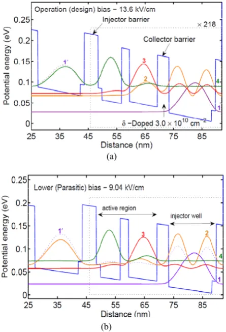
(anticrossing), one may devise a design that reduces this anticrossing and hence the parasitic current density which in turn reduces the threshold current density. One way to implement this is to separate the injector state from the lower parasitic states spatially, as performed in the diagonal design of [2], which was pointed out earlier in Section 1. Modifying this diagonal design, we have reduced the anticrossing almost 50% of the value reported by [2]. Furthermore, by devising a strategy we have detuned the lower laser state from the upper collector state, which in turn, has reduced the QCL gain linewidth. Fig. 1(a), illustrates the conduction band diagram of the QCL under the design bias of 13.6 kV/cm at which the injector level (1′) and the upper laser level (4) are in resonance. The operating temperature is assumed to be T=5 °K. The module consists of an Al0.17Ga0.83As/Al0.03Ga0.97As/GaAs/Al0.15 Ga0.85As/Al0.01Ga0.99As/Al0.15Ga0.85As/GaAs/Al0.03Ga0.97 As material system. As observed in Fig. 1(a), under the operating bias a diagonal radiative transition of frequency f≈E43/h ≈ 4.3 THz occurs from 4→3, while levels 3 and 2 are in coherent resonance tunneling. Note that h is the Planck′s constant. The collector level population, under goes a nonradiative depopulation process to level 1 that acts as the injector level to the next module. Energy of the nonradiative transition is absorbed by a longitudinal optical (LO) phonon of the same energy (i.e., E21=37.7 meV) in GaAs. Also seen in this figure are the extended wavefunctions for states 1′
and 4 with an energy splitting (injector anticrossing coupling) of ∆1′4=1.43 meV.
Figure 1(b) shows the QCL conduction band under the parasitic bias of 9.04kV/cm at which level 1′ from the preceding module is in resonance with the upper collector level (2) in the next module with anticrossing coupling of ∆1′2=0.29 meV. This has resulted in a
parasitic current channel due to LO phonon scattering from level 2 to 1.
Esmailifard et al: Design Optimization for 4.1-THZ Quantum Cascade Lasers 29
(a)
(b)
Fig. 1 Conduction band of the three-well active module with
the squared magnitude of the envelope wavefunctions obtained by the extended Hamiltonian approximation under (a) the operating bias of 13.6 kV/cm, and (b) a lower parasitic bias of 9.04 kV/cm, as characterized by the 1′→4 and 1′→2 alignments, respectively.
It is well known that, in a THz-QCL, the stronger the injector anticrossing the broader the gain spectrum is. In order to minimize the broadening effect, one needs to maintain the injector anticrossing in the range of
opt 1 4
1.4 meV<Δ′ <1.5 meV [4]− i.e., the optimized
injector anticrossing.
However, the injector, the collector, and the parasitic anticrossings that can be calculated for the three-well THz-QCL with diagonal transition fabricated by [2], as the reference points for comparison, are:
ref
1 4 2.23 meV,
Δ′ ≈ Δ ≈32ref 5 meV,
ref
1 2 0.54 meV
Δ′ ≈ and dipole
matrix element ref 43
z ≈3.7 nm.The superscript “ref” is to indicate the reference. In order to approach the optimized range, one may increase either the injector barrier height or width from the reference values. In the present design, in order to approachΔ1 4′ , and also keeping the parasitic anticrossing as low as possible, we have combined both techniques. As shown in Fig. 1, in addition to increase the injector barrier height by 18 meV (equivalent to an increase 2% in Al mole fraction),
with respect to those of the other two barriers in the module, we have added two 5-monolayer step-barriers of Al0.03Ga0.97As, on both sides of the injector barrier.
Furthermore, in order to increase the tunneling current through the collector barrier, as far as possible, the resonant coupling between levels 3 and 2 should also be as large as possible. The typical value of the collector coupling, ∆32, used in literature is in the range of 4 meV <∆32<5meV [4]. On the other hand, for ∆32>2 meV, the optical gain linewidth experiences an additional undesirable broadening.
As results of modifications, so far, we have achieved
∆1′4=1.43 meV, ∆32=4.94 meV, ∆1′2=0.29 meV,
∆1′3=0.38 meV and z43≈5.05 nm. Meanwhile, the
energy detuning δ32 (between energy levels 3 and 2) and δ1′4 (between energy levels 1′ and 4) are ignorable (i.e.,
the same as that of [2] ref ref
32 1 4 0
δ =δ′ = ). Notices, that in our design the parasitic anticrossing ∆1′2 is reduced to
half of the reference point. Hence, in the modified design, the parasitic current J1′2 is about one fourth of that obtained the reference diagonal design of [2]. Because for weak parasitic coupling, 2
1 2 1 2
J′ ∝(Δ′ ) [6].
In order to compensate for the undesirable broadening, caused by ∆32=4.94 meV, one may increase the collector energy detuning, δ32. In order to do that, we have raised the bottom of the second active well by about 8.9 meV. This is done by replacing the GaAs as the original well material used in [2] with Al0.01Ga0.99As. This has resulted in an energy detuning of δ32=4.38 meV which is not much less than E43=17.7 meV, as illustrated in Fig. 2(a).
In order to calculate the energy levels across the module, shown in this figure, we have used the tight-binding model for the resonant tunneling across the injector and the collector barriers. The integer number below each barrier/well layer indicates the number of monolayers forming that particular layer in the module. Each monolayer for this lattice matched system of materials is about 0.2825 nm. Using the energy levels and the wavefunctions illustrated in Fig. 2(a) we have calculated the radiative energy, E43, and the nonradiative depopulating energy, E21, versus the applied electric field. Figure 2(b) illustrates these variations in E43 and E21 versus the electric field. Also shown in this figure are the injector, collector and parasitic channels anticrossings (∆1′4, ∆32, ∆1′2, and ∆1′3)
that have been extracted from the results of Fig. 1 with extended wavefunctions. As also seen in this figure, the operation (design) bias coincides with the bias (13.6 kV/cm) at which injector anticrossing of ∆1'4=1.43 meV withzero detuning (δ1′4=0) occurs.
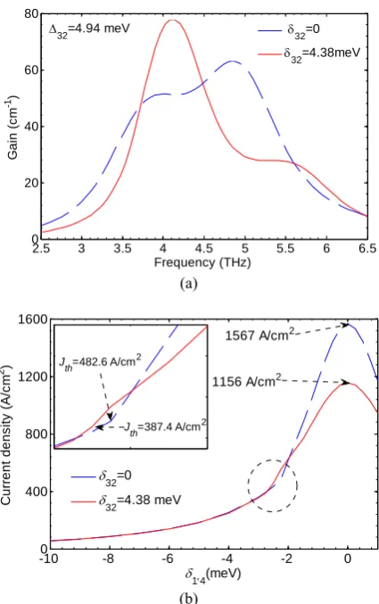
To investigate the effect of injector anticrossing and collector detuning on gain spectra broadening, we demonstrate the numerical results for the gain spectra as illustrated in Fig. 3(a). As observed in this figure, the dashed line represents the gain for ∆1'4=1.43 meV,
(b)
30 Iranian Journal of Electrical & Electronic Engineering, Vol. 7, No. 1, March 2011
(a)
(b)
Fig. 2 (a) Conduction band of the three-well active module
under the operating bias of 13.6 kV/cm, with the squared magnitude of the envelope wavefunctions obtained by the tight-binding approximation. (b) Anticrossings (calculated via extended Hamiltonian) and energy separations (obtained by tight-binding Hamiltonian), for the design.
∆32=4.94 meV, and δ32=0. That gain full width at half maximum is FWHM =2.1 THz and peak gain is 63.1 cm−1. For the final design in which the collector energy detuning is also increased to δ32=4.38 meV, the line broadening is reduced to FWHM=1 THz, while, the peak gain is increased to 77.81 cm−1 that occurs at the frequency of fpeak=4.1 THz (<E43/h). This shift in the frequency is due to the energy detuning (δ32).
Moreover, to investigate the effect of the energy detuning (δ32) on the steady state resonant-tunneling current through levels 1′ and 4, we have calculated the current density (J) versus δ1′4 (as illustrated in Fig.
3(b)). Note that δ1′4 is proportional to the external bias
[4]. The dashed and solid lines represent the current densities corresponding to the cases illustrated by the dashed and solid lines in Fig. 3(a), respectively.
For calculating these two curves, we have included the electron-photon interaction as well as the injector and collector anticrossings. While in analytic method of [2] the electron-photon interaction was ignored.
When carriers are injected through the collector barrier by means of resonant tunneling, the lifetime of
(a)
(b)
Fig. 3 (a) Optical gain for collector energy detuning of δ32=0
(dashed-line) and δ32=4.38 meV (solid line); (b) Steady state
resonant tunneling current density through levels 1′ and 4 versus δ1′4.
the lower laser level increases [4]. Also the electron-photon interaction beyond threshold reduces the lifetime of the upper laser level due to stimulated transitions. Both of these reduce the peak in the current density. Furthermore, the solid line demonstrates that when the collector detuning in the final design is increased to δ32=4.38 meV, the peak in current intensity decreases further. This detuning increases the lifetime of the lower laser level, which in turn, decreases the FWHM of the frequency linewidth due to scattering decreases [4]. This reduction in FWHM also reduces the resulting threshold current intensity (demonstrated by the inset in Fig. 3(b)). Notice, as the frequency linewidth due to scattering becomes narrower; the required population inversion, required for the threshold gain, becomes smaller. As shown in Fig. 3(b), in the absence of the collector detuning (δ32=0), Jth= 482.6 A/cm2. Whereas, the threshold current for the final design, with δ32=4.38 meV, is Jth= 387.4 A/cm2 that occurs at a smaller δ
1′4.
From Fig. 3(b), one can realize that the maximum current density Jmax and the dynamic range for lasing (Jmax/Jth) for the final design (with ∆1'4=1.43 meV and δ32=4.38 meV) are both reduced. On the other hand Fig. 3(a) shows that the laser gain is increased by 23.3%.
4.8 5.2 5.6
6 7 8 9 10 11 12 13 14 15
0 20 40
Bias (kV/cm) 1.0
2.0 3.0
Δ
E
(m
e
V
)
Δ
23=4.94meV
Δ
1′4=1.43meV
Δ
1′3=0.38meV
Δ
1′2=0.29meV
E 21
E 43
2.5 3 3.5 4 4.5 5 5.5 6 6.5
0 20 40 60 80
Frequency (THz)
Ga
in
(
c
m
-1)
δ
32=0
δ
32=4.38meV
Δ
32=4.94 meV
-100 -8 -6 -4 -2 0
400 800 1200 1600
δ
1′4(meV)
C
u
rr
ent
dens
it
y
(
A
/c
m
2)
δ
32=0
δ
32=4.38 meV
1567 A/cm2
1156 A/cm2
Jth=387.4 A/cm2
Jth=482.6 A/cm2
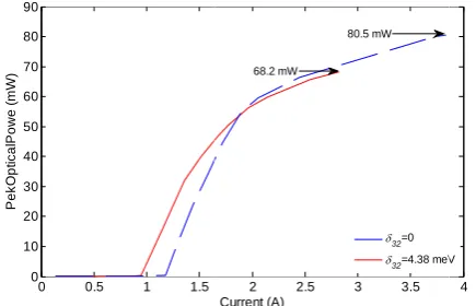
Esmailifard e Fig. 4 Peak op
detuning of δ3
Figure 4 design versu top contact g used by [2] cm2 and the The dashed l the laser in The values o peak current comparison design is abo data present differential q η=(e/ћω)·(dp structures wi 3 Conclusi We have radiative lin material syst threshold cu current chan to those of t parasitic cu injection se diagonal des Acknowledg This wo Telecommun Grant T-500-References
[1] Luo H Aers G cascad modul 04111 [2] Kumar
operat based Vol. 9 0 0.5 0 10 20 30 40 50 60 70 80 90 Pek O pt ic al Pow e ( m W )
et al: Design
ptical power ve
2=0 (dashed-lin
illustrates th us the device c
geometry is as with cross-se cavity mirror line in this fig absence of th of the peak p t densities ar shows that t out 15% less ed in this fig quantum effic pout/dI)~ 4.2 a ith δ32=4.38 m
ion
presented an newidth FW tem at 4.1TH urrent, higher nnels (i.e., 1′→ the earlier de urrent channe electivity for
ign.
gment
ork was su nication Rese
-10312.
H., Laframboi G. C. and Liu de lasers ba
le”, Appl. Phy 2–041114, 20 r S., Hu Q. ion of terah on a diagona 4, No. 13, pp.
5 1 1.5
Optimization f
ersus current fo ne) and δ32=4.3
he peak pow current (solid ssumed to be ectional area o loss is taken gure shows the
he collector d powers that c re labeled on the peak pow
than the case gure, we hav ciency is also and 4.9 photon meV δ32=0, res
optimized de WHM in the Hz. The design
peak gain, →2 and 1′→3 esign. As a re els have pro
the 1′→4
upported in earch Center
ise S. R., W u H. C., “Ter sed on a th ys. Lett., Vol 007.
. and Reno hertz quantum al design”, A . 131105–131
2 2.5 Current (A)
68.2 mW
for 4.1-THZ Q
or different ene 8 meV (solid li
wer for the fi line). The dev the same as t of A=2.448×1 to be αm=4 cm e peak power detuning (δ32=
orrespond to n the graph. T wer for the fi e δ32=0 Using ve calculated calculated to n/electron for spectively.
sign with narr e GaAs/AlGa
n shows a low smaller paras 3), in compari esult, the sma ovided a be tunneling in
part by I r (ITRC) un
Wasilewski Z. rahertz quantu hree-well act l. 90, No. 4,
J. L., “186 m-cascade las Appl. Phys. L
107, 2009.
3 3.5
δ32=0
δ32=4.38 meV
80.5 mW Quantum Casc ergy ne). final vice that 10−3 m−1. r for =0). the The final the the o be the row aAs wer sitic ison aller etter n a Iran nder R., um-tive pp. 6 K sers ett., [3] [4] [5] [6] (AD Tar inte opt Un and Au me Tel Tar cur Dev are Pho Nan Gra Far in l the app the ele 4 V cade Lasers ] Scalari G
Walther C quantum-c Phys. Lett 2009. ] Kumar S.
tunneling lasers”, P 245329, 2 ] Kumar S. quantum Appl. Phy 121125, 2 ] Sirtori C., L., Sivco tunneling Quantum 1729, Sep DSL), Departm rbiat Modares erests are mo toelectronic dev
niversity of Cal d the Universit ustralia, in 1987 mber of researc lecommunicatio rbiat Modares rrently a Profes
vice Simulation e Avalanche Ph otonic Crystals noelectronic D aphene nanorib rsi four books in laser electronic e best translatio plied sciences. M e two most pro
ctrical engineer
., Amanti M. C., Beck M. cascade laser t., Vol. 94, N
. and Hu Q., transport in Phys. Rev. B 2009.
., Williams B cascade laser ys. Lett., Vol. 2006.
, Capasso F. a o D.L. and
in quantum Electronics, p. 1998. Farnoush Tehran, Ira BSc degre from Semn and the M University Tehran, Ira working to Advanced ment of Electrica
University, odeling and s vices, and semic
Mohamm Farshi wa
He receiv degrees University Tehran, University (USC), L 1978, resp Ph. D deg lifornia at Sant ty of New Sou 7, respectively.
ch staff with the on Research
University (T sor of Electron n Lab (ADSL). hoto Diodes; A s and nanostru Devices base bbons. He has n the field of se s. His last trans n of the year in M. K. Moravve ominent profes ring, nationwid
I., Fischer M and Faist J emitting at 3 No. 4, pp. 041
, “Coherence terahertz quan B, Vol. 80,
B. S. and Hu rs with one-w
. 88, No. 12,
and Faist J., H Cho A. Y cascade lase Vol. 34, No.
Esmailifard
an, in 1976. Sh ee in electrica nan University, M.S. degree f of Science an an, in 2002. Sh
oward the Ph Device Sim al and Compute Tehran, Iran. imulation of conductor quan
mad Kazem
as born in Yazd ved the B. Sc. in physics y of Techno Iran, in 19 y of Southe Los Angeles, pectively, the M grees in electro ta Barbara (UC uth Wales (UN From 1980 to e Division of M
Center (ITRC TMU) in 1987 nics and head of
. His current fi All-optical dev uctures; Nanop d Carbon n s translated fro emiconductor d slation in 2004 w
n the field of e ej-Farshi was el ssors of 2002 i de. Professor M
31 M., Terazzi R., ., “Step well 3 THz”, Appl. 1114–041116,
of resonant-ntum-cascade pp.
245316-Q., “1.9 THz well injector”, pp.
121123-Hutchinson A. Y., “Resonant ers”, IEEE J. 9, pp.
1722-was born in he received the al engineering Iran in 1999, from the Iran nd Technology, he is currently .D. degree in mulation Lab er Engineering, Her research semiconductor ntum lasers.
Moravvej-d, Iran, in 1952. and the M. A. from Sharif ology (SUT), 76, and the ern California California, in M. Sc. and the onics from the CSB), in 1980, NSW), Sydney, 1984, he was a Microwave, Iran C). He joined , where he is f the Advanced elds of interest vices based on photonics; and nanotubes and om English to devices and one was selected as ngineering and lected as one of in the field of Moravvej Farshi , l , -e -z , -. t -n e g , n , y n b , h r -. . f , e a n e e , , a n d s d t n d d o e s d f f i
32
is currently a member of Op of the founde (OPSI). He ha for the period
department of Iran, in 199 submicron se interests are c optoelectronic modeling and nanotube field nanowire trans
a senior memb ptical Society o ers of the Optic as been elected
2009-2011.
Kamya
Iran, receive enginee Science the M. electric Modare 1999, f Electrical En
9. He has be emiconductor centered on th c devices. He is d simulation o d effect transisto
sistors.
Ira
ber of IEEE, of America (OS
cs and Photoni IEEE Iran Sect
ar Saghafi wa
on December ed the B. Sc. d ering from Ir e and Technol Sc. degree an cal engineering
es University, I respectively. ngineering of S
een working devices. His he physics of n
s presently wor of nano device ors, single elect
anian Journal
and also a se SA). He is also ics Society of tion Vice presid
as born in Teh r 19, 1963. degree in electr ran University logy in 1991, nd Ph.D. degre both from Tar Iran, in 1994 an He joined Shahed Univer
on simulation current resea nanoelectronic rking on numer es such as car tron transistors
of Electrical
nior one Iran dent
hran, He rical y of
and e in rbiat nd in the sity, n of
arch and rical rbon and
& Electronic Engineering, Vol. 7, No. 1, March 2011