www.adv-radio-sci.net/4/313/2006/ © Author(s) 2006. This work is licensed under a Creative Commons License.
Radio Science
From algorithm to implementation:
a case study on blind carrier synchronization
D. Schmidt, T. Brack, U. Wasenm ¨uller, and N. Wehn
Microelectronic System Design Research Group, University of Kaiserslautern, Erwin-Schr¨odinger-Straße, 67663 Kaiserslautern, Germany
Abstract. Increasing chip complexities demand a higher
design productivity. IP cores, which implement commonly needed operations, can help to dramatically shorten develop-ment and verification times for new designs. They often al-low for a efficient mapping of algorithmic tasks to a hardware architecture. In this paper we present a novel configurable building block for blind carrier synchronization that features combined frequency and phase offset estimation and an al-ternative modulation removal that improves communication performance compared to state-of-the-art designs. The used design flow exploits the benefits of IP cores for rapid devel-opment times while still offering the designer the full range of optimization possibilities for a specific design. It allowed us to do an almost complete design space exploration, assur-ing a near-optimal solution to the given problem. The imple-mentation platform is a XILINX Virtex II Pro FPGA.
1 Introduction
It is well known that the increasing chip complexities de-mand a higher design productivity. An important method for decreasing development effort and shortening development time is the use of IP cores. Many common building blocks, such as multipliers, dividers and dual port rams, can be ad-dressed by freely available IP cores. Configurability regard-ing precision, finite word lengths or throughput make them suitable for a wide range of designs, thus drastically reduc-ing engineerreduc-ing effort for design and verification.
This paper demonstrates the design of a configurable IP core for blind carrier synchronization with novel features (combined frequency and phase offset estimation, an ad-vanced modulation removal technique, and a configurable windowed spectral analysis). This building block is in use in a large scale communication system. The system through-Correspondence to: D. Schmidt ([email protected])
put requirements can not be fulfilled by a DSP and due to the low volume an FPGA solution is far more cost efficient than an ASIC implementation. Thus, XILINX Virtex II Pro FPGAs were selected as implementation platform. We used the freely available IP cores generated with the XILINX core generator tool. The case study shows the high level design flow from the basic algorithms of the application to the im-plemented building block. This design flow includes the mapping of algorithmic steps to the available IP cores and the evaluation of algorithmic variations, considering both, communications performance and implementation complex-ity. While designing a communication system the designer always has to trade off between these two. Our building block offers a configurable interface to accept different word lengths at the input.
Every inner receiver for wireless communication must estimate the generally unknown parameters of timing, fre-quency and phase offset of the received signal. All possi-ble negative influences introduced by them have to be elim-inated. As mentioned, this paper concentrates on the fre-quency and phase offset estimation and correction (carrier synchronization) of bursts with Phase Shift Keying modula-tion for different modulamodula-tion indicesM(MPSK), e.g.M=2 for BPSK andM=4 for QPSK.
Algorithm Selection and Optimization
IP Core Selection Parameter Selection
Fixed Point Simulations
Synthesis, MAP, P&R CP OK?
N
Y
Througput (TP) Estimation (Operations/Cycle)
TP OK?
Final Validation N
Y
OK? N
Y
Configuration Data Problem Description
XILINX IP Cores
Floating Point Simulations
FFT 1(N,q,x) FFT 2(N,q,x) FFT 3(N,q,x) CORDIC 1(x,y) CORDIC 2(x,y) SINCOSLUT(x) DIVIDER 1(x,y) DIVIDER 2(x,y) DUAL PORT RAM SINGLE PORT RAM DUAL PORT ROM SINGLE PORT ROM MACC(x,...) DCT(x) CAM(x)
SHIFT REGISTERS ...
CP: communications performance TP: throughput
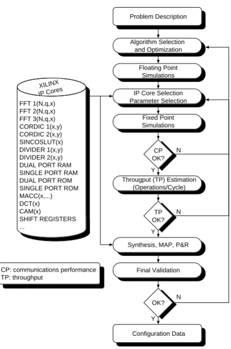
Figure 1: The used design flow for IP core based design
Figure 1: The used design flow for IP core based design
quirement specifications. A first estimate of the communications performance of an
algorithm can be derived using a floating point model. The use of a high level
mod-eling language, like SystemC or MATLAB, allows for faster development and shorter
simulation times compared to a VHDL model. These first models are neither cycle
accurate nor bit true models of the later implementation. Once an algorithm achieving
a sufficient communications performance is found, the different implementation
alter-natives have to be reviewed. Thus a more accurate fixed point model of the hardware is
needed that takes into account the effects of different quantization levels and of the IP
cores used. Cores from the XILINX IP core library can be used to reduce development
effort. To evaluate the impact of the decisions made on the communications
perfor-mance, the simulation results of the fixed point model are compared to the results of
the floating point simulation. The fixed point models can still be written in a high level
language.
The core library provides IP cores for many high latency operations like FFTs or
dividers. In cases where the number of clock cycles needed to perform a calculation
is dominated by such complex operations, a rough throughput estimation can be done
Fig. 1. The used design flow for IP core based design.
2 Design flow
Figure 1 shows the used design flow. Typically any given problem can be solved with various algorithms. Additionally, each of the algorithmic alternatives may depend on several parameters. There may also be different ways to implement an algorithm using different IP cores. Hence, all implemen-tation alternatives form a tree, the so called design space. In the phase of design space exploration the designers task is to select the algorithm, the parameters and the IP cores to solve the problem under all given constraints. In a commu-nication system these constraints usually regard the imple-mentation complexity, the minimum throughput and maxi-mum latency as well as the achievable communications per-formance. As the characteristics of each algorithmic alter-native are not known in advance it is necessary to estimate them for each algorithm under consideration until a feasible solution is found. This is indicated by the iterative loops in the design flow diagram.
To minimize the time spent for design space exploration it is vital to exclude as many implementation alternatives as early in the process as possible. This is best done by
eval-uating the communications performance of each algorithm prior to the time consuming estimation of the implementa-tion complexity and comparing it to the requirement specifi-cations. A first estimate of the communications performance of an algorithm can be derived using a floating point model. The use of a high level modeling language, like SystemC or MATLAB, allows for faster development and shorter simu-lation times compared to a VHDL model. These first models are neither cycle accurate nor bit true models of the later im-plementation. Once an algorithm achieving a sufficient com-munications performance is found, the different implementa-tion alternatives have to be reviewed. Thus a more accurate fixed point model of the hardware is needed that takes into account the effects of different quantization levels and of the IP cores used. Cores from the XILINX IP core library can be used to reduce development effort. To evaluate the impact of the decisions made on the communications performance, the simulation results of the fixed point model are compared to the results of the floating point simulation. The fixed point models can still be written in a high level language.
The core library provides IP cores for many high latency operations like FFTs or dividers. In cases where the number of clock cycles needed to perform a calculation is dominated by such complex operations, a rough throughput estimation can be done based on the specifications of the used IP cores. The glue logic does not significantly contribute to the compu-tation complexity or the implemencompu-tation complexity. Hence, to estimate the number of occupied slices, it is sufficient to instantiate and connect the main blocks of the design. Then, only for the design with the optimal trade-off a synthesizable VHDL-model has to be described and validated.
As a last step the resulting design has to be verified using the fixed point model. In the area of communication systems this can either be done with a bit true C-model or by com-parison of statistical bit error rates. After synthesis, mapping and place and route have been performed, a final validation of throughput and area ensure the compliance with the given constraints.
3 Problem description
This section contains all fundamental algorithms needed for the development of our blind carrier synchronization build-ing block. Further details and resources can be found in Meyr et al. (1997); Viterbi and Viterbi (1983); Mengali and D’Andrea (1997); van Trees (1968); Barry et al. (2004). The basic synchronization steps are estimation of the frequency offset, frequency offset correction, estimation of the phase offset and correction of the phase offset.
In an MPSK modulation scheme the set of M possible symbolssmis given by:
sm:=e j2πM·m
The received sample sequencer is given in the complex baseband according to Eq. (2):
r(l):=s(l)·ej (2πfolT+8)+n(l) l=0,1, .., L−1 (2) The sample sequencer withLelements is based on MPSK symbolsswith one sample per symbol and symbol duration
T, and is disturbed by a noise sequencen. The frequency off-setfoand phase offset8have to be estimated and corrected.
They are considered fixed during one burst transmission. The estimation of the unknown parametersfoand8can
be done by data aided or non data aided methods. Data aided methods need known symbols in the transmitted bursts. The introduced redundancy is exploited to estimate the frequency and phase offset, at the cost of decreasing bandwidth and power efficiency (Meyr et al., 1997). Hence, non data aided or blind methods become mandatory. They estimate the pa-rameters without the help of such a training sequence. In this case especially estimation of frequency offset becomes a very critical task with high impact on communications per-formance. Deviation of the frequency estimation results in bursts with high bit error rates, resulting in high frame error rates after channel decoding.
For blind frequency or phase offset estimation the mod-ulation introduced by the unknown transmitted symbol se-quence s has to be removed from the received sample se-quencer. State-of-the-art modulation removal is based on a power ofM operation onr, where M is the modulation index.
˜
r(l):=r(l)M = |r(l)|M ·ej M·arg(r(l)) (3)
l=0,1, .., L−1
Note that by such a power ofMoperation all the MPSK sym-bols defined in Eq. (1) are transformed to the symbols0. Af-ter the modulation has been removed, an approximation of the maximum likelihood estimation of the frequency offset can be found by calculating the spectral power of the se-quencer˜. This is done by performing a Fast Fourier Transfor-mation (FFT) (Mengali and D’Andrea, 1997) withN points according to Eq. (4):
X(k):=
N−1
X
n=0
x(n)·e−j
2π·k·n N
k=0,1, .., N −1 (4)
The sequencexwithNelements corresponds to the sequence ˜
rwithL≤N elements of Eq. (4), which is padded with ze-ros to achieve theN elements of Eq. (4). Note that each bin X(k)represents the spectral power of x in a range of
(M·N·T )−1Hz, not only in one distinct frequency. This results in a loss of accuracy, depending on the numberN of points. The estimated frequency offsetf˜ois given by spectral
analysis of the FFT output, i.e. the FFT bin corresponding to the estimated frequency offset is given by:
kf, s.t.: |X(kf)| =max k
|X(k)| k=0,1, .., N−1 (5)
After spectral analysis of the FFT bins, the sample sequence
rmust be corrected with the calculated frequency offsetf˜
o.
The corrected sample sequenceuis then given by:
u(l):=r(l)·e
−j
2π·kf·l M·N
l=0,1, .., L−1 (6) Phase offset estimation can be done using the V and V algorithm presented in Viterbi and Viterbi (1983). This algo-rithm requires the modulation to be removed from the sample sequenceu, analogous to Eq. (4):
˜
u(l):=u(l)M l=0,1, .., L−1 (7)
The phase offset of the sample sequenceuis then estimated to be the average phase of the symbols in the sequenceu˜, as given in Eq. (8):
˜
8:=M−1·arg
L−1
X
l=0 ˜
u(l) (8)
The sequence u(l)must be corrected with the estimated phase offset8˜, which results in
v(l):=u(l)·e−j8˜ l=0,1, .., L−1 (9)
Equation (8) still leaves an M-time phase ambiguity. Apart from this phase ambiguity the sequencev(l)gives an estimation of the transmitted symbolss(l). The resolution of the phase ambiguity can be achieved using several methods, e.g. differential encoding can be used. But this strongly de-pends on the actual communication system. Thus this step of the synchronization process is not considered in our case study.
4 Algorithm optimization
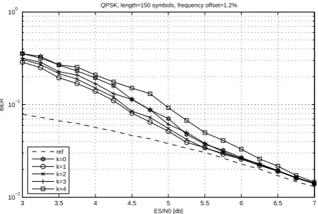
During the design space exploration we reviewed several modifications of the above mentioned algorithms. As men-tioned, we were particularly interested in their impact on im-plementation complexity and communications performance. Since the power operation for modulation removal in Eqs. (4) and (7) enhances the noise in the signal super pro-portional, so called self noise is inferred. This results in large frequency offset estimation errors especially at medium to low signal to noise ratio ranges. Thus bursts with high bit error rate and therefore high frame error rate after channel decoding result.
To elude this problem another approach for removing the modulation, proposed in Wang et al. (2003); Viterbi and Viterbi (1983), is used. This technique for modulation re-moval is based on the following calculation:
˜
r(l): = |r(l)|k·ej M·arg(r)
k=0,1, .., M;l=0,1, .., L−1 (10)
3 3.5 4 4.5 5 5.5 6 6.5 7 10−2
10−1 100
QPSK, length=150 symbols, frequency offset=1.2%
ES/N0 [db]
BER
ref k=0 k=1 k=2 k=3 k=4
Figure 1: BER of 150 symbols QPSK bursts for different values of kFigure 2: BER of 150 symbols QPSK bursts for different values of k
of the simulation results to a perfect frequency and phase synchronization reflecting the performance limits of the AWGN channel. Clearly,k= 1yields the best performance. Simulations with different burst lengths and BPSK bursts showed similar results. A de-tailed discussion of the presented algorithms regarding communications performance can be found in [7].
The frequency and phase estimation can be performed in a combined manner de-fined by Equation 11 or in a separate manner, dede-fined by Equation 6, Equation 7 and Equation 8. Obviously, the combined frequency and phase offset estimation reduces the overall computational complexity. Simulation results also showed that using differ-ent modulation removal techniques for frequency and phase offset estimation does not yield a better communications performance.
5
IP Core Selection
To obtain a first estimate of the number of slices occupied by each implementation alternative, a VHDL-model that merely instantiates and connects the needed IP cores and all major building blocks, is used. The time consuming task of describing all the needed control logic and validating the design is not yet necessary at this stage, because for computational intensive algorithms, like the ones under consideration, the control logic does not significantly contribute to the implementation complexity.
The components of the synchronization circuit are derived from the optimized al-gorithm and mapped to XILINX IP cores. We also used specific XILINX resources like the internal multipliers (MULT) and block RAM (BRAM) available on the Virtex II Pro FPGA.
For the FFT calculation defined in Equation 4 three XILINX IP cores with differ-ent architectures are available [8]. The architectures differ in throughput, latency and needed resources. Due to the throughput requirements we had to choose the fastest FFT core with a throughput of one FFT bin calculation per clock cycle independent of
7
Fig. 2. BER of 150 symbols QPSK bursts for different values of k.
The calculation of the phase offset 8˜ can be simpli-fied with further algebraic transformations. Combining Eqs. (6–8) gives an equivalent equation for calculating the estimated phase offset8˜:
˜
8:=M−1·arg(X(kf)) (11)
Equation (11) uses the FFT result of Eq. (4) for the bin k
withk=kf. Thus frequency and phase offset estimation can
be combined efficiently. Note that in this case phase offset estimation and frequency offset estimation implicitly use the same technique for modulation removal. The input burst has to be corrected with the estimated values of frequency and phase offset, formally described as:
v(l):=r(l)·e
−j
2π kf·n M·N
+ ˜8
l=0,1, .., L−1 (12) If the range of the occurring frequency offset is known in advance, the communications performance can be improved significantly by simply limiting the spectral analysis. This windowing technique is given by substitutingkf in Eq. (12)
withkf wfrom Eq. (13): kf w, s.t.: |X(kf w)| =max
k
|X(k)|
k=0, .., wu, wl, .., N−1 (13)
The parameterswuandwldefine the FFT bin range, where
the frequency offset has to be found. SettingwutoN/2−1
andwltoN/2 describes the FFT binkf given in Eq. (5).
Evaluating the impact of the parameterkon communica-tions performance is done by simulation. Figure 2 shows the bit error rates (BER) of QPSK bursts with a length of 150 symbols for the different modulation removal techniques. We simulated transmission of the bursts over an additive white Gaussian noise (AWGN) channel using a floating point model written in C. A reference graph ref is provided to allow comparison of the simulation results to a perfect frequency and phase synchronization reflecting the performance lim-its of the AWGN channel. Clearly, k=1 yields the best
performance. Simulations with different burst lengths and BPSK bursts showed similar results. A detailed discussion of the presented algorithms regarding communications per-formance can be found in Brack et al. (2004).
The frequency and phase estimation can be performed in a combined manner defined by Eq. (11) or in a separate man-ner, defined by Eqs. (6–8). Obviously, the combined fre-quency and phase offset estimation reduces the overall com-putational complexity. Simulation results also showed that using different modulation removal techniques for frequency and phase offset estimation does not yield a better communi-cations performance.
5 IP core selection
To obtain a first estimate of the number of slices occupied by each implementation alternative, a VHDL-model that merely instantiates and connects the needed IP cores and all major building blocks, is used. The time consuming task of de-scribing all the needed control logic and validating the design is not yet necessary at this stage, because for computational intensive algorithms, like the ones under consideration, the control logic does not significantly contribute to the imple-mentation complexity.
The components of the synchronization circuit are derived from the optimized algorithm and mapped to XILINX IP cores. We also used specific XILINX resources like the inter-nal multipliers (MULT) and block RAM (BRAM) available on the Virtex II Pro FPGA.
For the FFT calculation defined in Eq. (4) three XILINX IP cores with different architectures are available (Xilinx, 2003a). The architectures differ in throughput, latency and needed resources. Due to the throughput requirements we had to choose the fastest FFT core with a throughput of one FFT bin calculation per clock cycle independent of the pa-rameterk. The number of FFT points must be chosen to be at least twice the maximum burst length in the application Mengali and D’Andrea (1997). It also has to be considered that more points result in a higher resolution of the FFT bins and hence in a higher estimation accuracy.
Table 1. Selected alternatives for modulation removal and their IP
core and resource requirements.
Alt. Equation Cores MULT SLICES
0 α:=ej4arg(r) aCORDIC, SCL 0 273
1 |r| ·α CORDIC, SCL 2 331
2a r4/(<(r)2+ =(r)2) DIVIDER 10 297
2b α(<(r)2+ =(r)2) aCORDIC, SCL 4 290
2c |r|2·α CORDIC, SCL 3 325
3 |r|3·α CORDIC, SCL 4 329
4 r4 6 79
In some cases ofk andMthe use of a CORDIC module obsolete. Fork=M Eq. (10) reduces to a power ofM op-eration, which can be implemented using 3 multipliers in the case of BPSK and 6 multipliers for QPSK modulation.
ForM=4 andk=2 Eq. (10) equalsr˜=r4/|r|2. To calcu-late|r|2= <(r)2+ =(r)2two multipliers are needed, so the CORDIC module can be replaced by 10 Multipliers and a di-vider. As a third alternative fork=2, we can use a simplified CORDIC module (aCORDIC) that only calculates arg(r)but not|r|. Then, again, we need two additional multipliers to calculate|r|2. The simplified CORDIC module is also suf-ficient to perform the calculation of Eq. (10) in the case of
k=0.
After modulation removal the resulting sample sequencer˜ has to be transformed back to Cartesian coordinates for the FFT calculation (see Eq. (4)). This is accomplished with a sine-/cosine-look-up-table (SCL) (Xilinx, 2002), also avail-able as an IP core, and internal multipliers to realize the
ej xoperation.
The realization of Eq. (5) as well as the improved version, defined in Eq. (13), is not based on IP cores. The windowing feature proposed in Eq. (13) to evaluatekf wis realized using
a limited maximum absolute value search on the determined FFT bins. This can be implemented in a very efficient way using only counters and comparators. Since this part does not differ between two algorithmic alternatives, it does not have to be taken into account when comparing their imple-mentation complexities.
After determining the frequency binkf w, the phase offset
is estimated according to Eq. (11). Again, the argument func-tion needed for this equafunc-tion is realized with a CORDIC IP core. Because only one argument calculation per phase esti-mation has to be performed, we can use a rather small serial aCORDIC core without the ability to calculate|r|.
Rotation of the samples, as described, in Eq. (12) is ac-complished with complex number multiplications and a
sec-modulation
removal FFT spectralanalysis
RAM phase/freq.
correction
AGC IP CORE phasefinal
rinp ˜s
˜r X(k)
r
r Φ, k
fw
rram
v
v
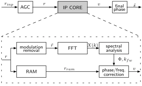
Figure 1: Base architecture for blind carrier synchronization
Figure 3: Base architecture for blind carrier synchronization
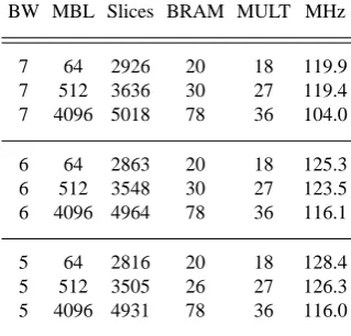
BW MBL Slices BRAM MULT MHz
7 64 2926 20 18 119.9
7 512 3636 30 27 119.4
7 4096 5018 78 36 104.0
6 64 2863 20 18 125.3
6 512 3548 30 27 123.5
6 4096 4964 78 36 116.1
5 64 2816 20 18 128.4
5 512 3505 26 27 126.3
5 4096 4931 78 36 116.0
Table 2: Synthesis results
performance of each implementation alternative based on high level simulations (in SystemC/MATLAB) and the specifications of the used IP cores. The time demanding step of describing and verifying a fully functional and synthesizable VHDL-model has only to be done for the final architecture. Thus, the IP core based design flow proved to combine near optimal results with very short development times.
7
Conclusion
In this paper we presented a configurable building block that utilizes advanced tech-niques like combined frequency and phase synchronization, improved modulation re-moval and a windowed spectral analysis. These features yield high throughput, com-pact size and best communications performance achievable for transmissions without training sequence. We used a design flow suitable for a wide range of designs. In our case study we showed how to employ it to efficiently explore the design space for a blind frequency and phase synchronization module for MPSK bursts.
10
Fig. 3. Base architecture for blind carrier synchronization.
ond SCL.
The considered implementation alternatives for modula-tion removal and the IP cores needed by each of them are listed in Table 1. It also shows the number of slices and other hardware resources occupied. The resources needed by the FFT and for the other building blocks (phase offset estima-tion, spectral analysis with windowing and combined correc-tion) are not taken into account, because they are the same for all values ofk.
6 Results
We used XILINX ISE 6.1 for synthesis and place and route with XILINX Virtex II Pro FPGA XC2VP50 as target plat-form. Figure 3 shows the main building blocks of the im-plemented architecture. We assume that the input signal is filtered using a matched filter and is sampled at one sam-ple per symbol. As a front-end to the IP core an automatic gain control unit (AGC) is required to adapt the input sam-ples bit width to the IP core input bit width without limiting the dynamic range. The back-end must deal with the M-times phase uncertainty introduced by Eq. (8).
The building blocks modulation removal, FFT, spectral analysis, and phase/freq. correction correspond directly to the algorithms from Sect. 3 and Sect. 4. The RAM buffer is used to guarantee constant throughput by hiding the FFT latency.
The final working and validated IP core is configurable regarding different bit widths (BW) of the input signalrand maximum burst lengths (MBL). As can be seen in Table 2 the size of the IP core grows strongly with increasing MBL due to the FFT component. The results also show that the over-head introduced by the alternative modulation removal with
Table 2. Synthesis results.
BW MBL Slices BRAM MULT MHz
7 64 2926 20 18 119.9
7 512 3636 30 27 119.4
7 4096 5018 78 36 104.0
6 64 2863 20 18 125.3
6 512 3548 30 27 123.5
6 4096 4964 78 36 116.1
5 64 2816 20 18 128.4
5 512 3505 26 27 126.3
5 4096 4931 78 36 116.0
The resulting maximum sample throughput is about half the clock speed because the FFT point size is at least twice the maximum burst length (Sect. 5). Thus the corresponding bit rate is determined by the modulation:
throughput[bits/sec] ≈(2·cycle)−1·log2(M) (14) For example, using QPSK modulation Eq. (14) evaluates to a bit rate beyond 100 Mbps for every configuration (Table 2). We have also shown that an IP core based design flow al-lows not only for a rapid implementation but also for a fast and exhaustive design space exploration. As in many designs resource needs and throughput are dominated by operations that can be covered with pre-existing IP cores, it is possible to quickly and accurately estimate the performance of each implementation alternative based on high level simulations (in SystemC/MATLAB) and the specifications of the used IP cores. The time demanding step of describing and verifying a fully functional and synthesizable VHDL-model has only to be done for the final architecture. Thus, the IP core based design flow proved to combine near optimal results with very short development times.
7 Conclusions
In this paper we presented a configurable building block that utilizes advanced techniques like combined frequency and phase synchronization, improved modulation removal and a windowed spectral analysis. These features yield high throughput, compact size and best communications per-formance achievable for transmissions without training se-quence. We used a design flow suitable for a wide range of designs. In our case study we showed how to employ it to efficiently explore the design space for a blind frequency and phase synchronization module for MPSK bursts.
References
Barry, J. R., Lee, E. A., and Messerschmitt, D. G.: Digital Commu-nication, Kluwer Acad. Publishers, Boston/Dordrecht/London, 2004.
Brack, T., Wasenm¨uller, U., Schmidt, D., and Wehn, N.: De-sign Space Exploration for Frequency Synchronisation of BPSK/QPSK Bursts, in Kleinheubacher Berichte, 48, 337–341, 2004.
Mengali, U. and D’Andrea, A.: Synchronization Techniques for Digital Receivers, Plenum Publ. Corp., New York, 1997. Meyr, H., Moeneclaey, M., and Fechtel, S.: Digital Communication
Receivers, Wiley and Sons, Inc., New York, 1997.
van Trees, H. L.: Detection, Estimation and Modulation Theory, Wiley and Sons, Inc., New York, 1968.
Viterbi, A. J. and Viterbi, A. M.: Nonlinear Estimation of PSK Modulated Carrier Phase with Application to Burst Digital Transmission, IEEE Trans. on Inf. Theory, 32, 543–551, 1983. Volder, J.: The CORDIC Trigonometric Computing Technique, IRE
Transactions on Electronic Comp., 8, 330–334, 1959.
Wang, Y., Serpedin, E., and Ciblat, P.: Optimal Blind Carrier Re-covery for MPSK Burst Transmissions, IEEE Trans. on Com-mun., 51, 1571–1581, 2003.
Xilinx Inc. Fast Fourier Transform v2.0, Mar. 2003a. Xilinx Inc. CORDIC v2.0, Mar. 2003b.