(Full length research article)
Design a Microstrip Patch Antenna with Electronic Band gap Structure for
Wireless Devices
M A Khana, Tazeem A Khanb and M. T Begc
aHead, Electrical Engg Section, F/o Engg & Tech., JMI bE & C Deptt., F/o Engg & Tech., JMI c
Prof & Head, E & C Deptt., F/o Engg & Tech., JMI
Received 15 June 2012; accepted 20 June 2012, Available online 30 June 2012
Abstract
To design a compact microstrip patch antenna for use in wireless/cellular devices. A typical cellular phone measures about 14.5 cm by 4.5 cm. Hence the antenna designed must be able to fit in such a cellular phone. I have to design a compact microstrip patch antenna having a center frequency of 2.5 GHz accordingly to reach the design and results. The ground plane dimensions for the patch antenna has been designed to be 28 mm by 28 mm and the patch dimensions are 28 mm by 28 mm. Hence the antenna is compact enough to be placed in a typical cellular phone. I have to plot the radiation pattern for the desired antenna orientation and back lobe radiation also to be reduced.
Key Words: Patch antenna, Microstrip
1. Introduction
1Micro strip patch antennas have some Limitations such
as restricted band-width of operation, low gain and a potential decrease in radiation efficiency due to surface wave losses. The ability of an Electronic band gap Structure or Photonic band gap Substrate to minimize the surface wave effects is analyzed for a thick and high εr substrate. The thickness of the dielectric substrate being used, increases, surface waves and spurious feed radiation also increases, which hampers the bandwidth of the antenna. The return-loss going to be minimized with the increasing of the Electronic band gap structure
2. Microstrip patch antenna
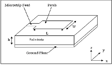
In its most basic form, a Microstrip patch antenna consists of a radiating patch on one side of a dielectric substrate which has a ground plane on the other side as shown in Figure 1.The patch is generally made of conducting material such as copper or gold and can take any possible shape. The radiating patch and the feed lines are usually photo etched on the dielectric substrate. In order to simplify analysis and performance prediction, the patch is generally square, rectangular, circular, triangular, and elliptical or some other common shape as shown in Figure 2.
* Corresponding author's email: [email protected]
Fig.1 Structure of a microstrip Patch Antenna
For a rectangular patch, the length L of the patch is usually- 0.3333λ0< L< 0.5λ0, where λ0 is the free-space wavelength. The patch is selected to be very thin such that t << λ0 (where t is the patch thickness). The height h of the dielectric substrate is usually 0.003 λ0≤h ≤0.5 λ0. The dielectric constant of the substrate (εr) is typically in the range 2.2≤ εr ≤12. The basic shapes that the patch can take are
Microstrip patch antennas radiate primarily because of the fringing fields between the patch edge and the ground plane. For good antenna performance, a thick dielectric substrate having a low dielectric constant is desirable since this provides better efficiency, larger bandwidth and better radiation [5].
Fig. 2 Common shape of a microstrip Patch elements
However, such a configuration leads to a larger antenna size. In order to design a compact Microstrip patch antenna, higher dielectric constants must be used which are less efficient and result in narrower bandwidth. Hence a compromise must be reached between antenna dimensions and antenna performance.
3. Methods of analysis
The most popular models for the analysis of Microstrip patch antennas are the transmission line model, cavity model, and full wave model [5] (which include primarily integral equations/Moment Method). The transmission line model is the simplest of all and it gives good physical insight but it is less accurate. The cavity model is more accurate and gives good physical insight but is complex in nature. The full wave models are extremely accurate, versatile and can treat single elements, finite and infinite arrays, stacked elements, arbitrary shaped elements and coupling. These give less insight as compared to the two models mentioned above and are far more complex in nature.
3.1 Transmission Line Model
This model represents the microstrip antenna by two slots of width W and height h, separated by a transmission line of length L. The microstrip is essentially a non-homogeneous line of two dielectrics, typically the substrate and air.
Fig. 3 Microstrip line & Electric Field Line
Hence, as seen from Figure 6, most of the electric field lines reside in the substrate and parts of some lines in air.
As a result, this transmission line cannot support pure transverse-electric-magnetic (TEM) mode of transmission, since the phase velocities would be different in the air and the substrate. Instead, the dominant mode of propagation would be the quasi-TEM e mode. Hence, an effective dielectric constant (reff) must be obtained in order to account for the fringing and the wave propagation in the line. The value of is slightly less then because the fringing fields around the periphery of the patch are not confined in the dielectric substrate but are also spread in the air as shown in Figure 3 above. The expression for reff is given by Balanis [12] as:
Where ref = Effective dielectric constant r = Dielectric constant of substrate h = Height of dielectric substrate W = Width of the patch
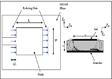
Consider Figure 4 below, which shows a rectangular microstrip patch antenna of length L, width W resting on a substrate of height h. The co-ordinate axis is selected such that the length is along the x direction, width is along the y direction and the height is along the z direction.
Fig.4 Microstrip patch Antenna
Fig. 5.Top & Side View of antenna
It is seen from Figure 5 that the normal components of the electric field at the two edges along the width are in opposite directions and thus out of phase since the patch is / 2 long and hence they cancel each other in the broadside direction. The tangential components (seen in Figure 5), which are in phase, means that the resulting fields combine to give maximum radiated field normal to the surface of the structure. Hence the edges along the width can be represented as two radiating slots, which are / 2 apart and excited in phase and radiating in the half space above the ground plane. The fringing fields along the width can be modeled as radiating slots and electrically the patch of the microstrip antenna looks greater than its physical dimensions. The dimensions of the patch along its length have now been extended on each end by a distance L, which is given empirically by Hammers tad [13] as:
The effective length of the patch L ef f now becomes:
For a given resonance frequency f o , the effective length is given by [9] as:
For a rectangular Microstrip patch antenna, the resonance frequency for any TMmn mode is given by James and Hall [14] as:
Where m and n are modes along L and W respectively. For efficient radiation, the width W is given by Bahl and Bhartia [15] as:
3.2 Cavity Model
Although the transmission line model discussed in the previous section is easy to use, it has some inherent disadvantages. Specifically, it is useful for patches of rectangular design and it ignores field variations along the radiating edges. These disadvantages can be overcome by using the cavity model. A brief overview of this model is given below. In this model, the interior region of the dielectric substrate is modeled as a cavity bounded by electric walls on the top and bottom. The basis for this assumption is the following observations for thin substrates (h << )[10].
• Since the substrate is thin, the fields in the interior region do not vary much in the z direction, i.e. normal to the patch.
• The electric field is z directed only, and the magnetic field has only the transverse components Hx and Hy in the region bounded by the patch metallization and the ground plane. This observation provides for the electric walls at the top and the bottom.
Fig.6 Charge distribution and current density creation on the microstrip patch
movement, currents flow at the top and bottom surface of the patch. The cavity model assumes that the height to width ratio (i.e. height of substrate and width of the patch) is very small and as a result of this the attractive mechanism dominates and causes most of the charge concentration and the current to be below the patch surface. Much less current would flow on the top surface of the patch and as the height to width ratio further decreases, the current on the top surface of the patch would be almost equal to zero, which would not allow the creation of any tangential magnetic field components to the patch edges. Hence, the four sidewalls could be modeled as perfectly magnetic conducting surfaces. This implies that the magnetic fields and the electric field distribution beneath the patch would not be disturbed. However, in practice, a finite width to height ratio would be there and this would not make the tangential magnetic fields to be completely zero, but they being very small, the side walls could be approximated to be perfectly magnetic conducting [5].
Since the walls of the cavity, as well as the material within it are lossless, the cavity would not radiate and its input impedance would be purely reactive. Hence, in order to account for radiation and a loss mechanism, one must introduce a radiation resistance Rr and a loss resistance R L. A lossy cavity would now represent an antenna and the loss is taken into account by the effective loss tangent eff which is given as:
QT is the total antenna quality factor and has been expressed by [4] in the form:
• Qd represents the quality factor of the dielectric and is given as:
Where, r is the angular resonant frequency. W Tis the total energy stored in the patch at resonance. P d is the dielectric loss.
tan is the loss tangent of the dielectric.
• Qc represents the quality factor of the conductor and is given as:
Where, P c is the conductor loss. is the skin depth of the conductor. h is the height of the substrate.
•Qr represents the quality factor for radiation and is given as:
Where Pr is the power radiated from the patch.
Substituting equations (3.8), (3.9), (3.10) and (3.11) in equation (3.7), we get
Thus, (3.12) describes the total effective loss tangent for the microstrip patch antenna.
4. Patch antenna design and simulation result
4.1 design specifications
Dielectric constant of substrate (εr) = 4.6 Height of substrate (h) = 1.6mm Frequency of Operation (fo) = 2.5 GHz
c = velocity of light = 3x10(8) m/s or = 3x10(11) mm/s
So, for a Square patch Antenna the Length and Width is taken as 28mm.
Width (W) = Length (L) =28mm
Depth of the slot for inset feed is given by Yo = 10 mm
4.2 Design procedure
4.2.1 Design specifications
The three essential parameters for the design of a Microstrip Patch Antenna are:
Frequency of operation(fo): The resonant frequency of the antenna must be selected appropriately. The resonant frequency selected for my design is 2.5 GHz.
Dielectric constant of the substrate (εr): The dielectric material selected for my design is glass (FR4) which has a dielectric constant of 4.6. A substrate of a high dielectric constant when selected reduces the dimensions of the antenna.
Height of dielectric substrate (h): For the microstrip patch antenna to be used in cellular phones, it is essential that the antenna is not bulky. Hence, the height of the dielectric substrate is selected as 1.6 mm.
4.2.2 Design steps
Step 1: Calculation of the Width (W):
The width of the Microstrip patch antenna is given by the equation
1 2
2
r o
C W
f
Step 2: Calculation of Effective dielectric constant (εreff)
The effective dielectric constant is given by the equation
1 2
1 1
1 12
2 2
r r
reff
h W
Step 3: Calculation of the Effective length (Leff)
The effective length is calculated by the equation
2
eff
LL L 2 0
eff
reff
C L
f
Step 4: Calculation of the length extension (∆L):
( 0.3) 0.264
0.412
( 0.258) 0.8
reff
reff
W h L h
W h
Step 5: Calculation of actual length of patch (L):
The actual length is obtained by the equation
2
effL
L
L
Step 6: Calculation of the ground plane dimensions (Lg
and Wg):
The transmission line model is applicable to infinite ground planes only. However, for practical considerations, it is essential to have a finite ground plane. It has been shown that similar results for finite and infinite ground plane can be obtained if the size of the ground plane is greater than the patch dimensions by approximately six times the substrate thickness all around the periphery. Hence, for this design, the ground plane dimensions would be given as:
Specification
Frequency : 2.5GHz Return Loss : >20dB Gain : >6 dB VSWR : 1:1.3 εr : 4.6 Thickness : 1.6mm
5. Simulation results
Microstrip Patch Antenna without EBG Structure For 2.5 Ghz
Microstrip Patch Antenna with a Single EBG Structure for 2.5 Ghz
An electronic bandgap has been made at the following specified location:
X = 0 mm; Y = 7 mm: Radius = 1mm.
An electronic bandgap has been made at the following specified location:
X = -7.5 mm; X = 0 mm;X = 7.5 m Y = 5 mm:Y = 7 mm; Y = 5 mm; Radius=1.5mmRadius=1mm.Radius= 1.2mm.
Microstrip Patch Antenna with a Three Different EBG Structure for 2.5 GHz
An electronic bandgap has been made at the following specified location:
X = -7.5 mm; X = 0 mm;X = 7.5 Y = 5 mm;Y = 7 mm; Y = 5 mm;
Radius = 1mm Radius = 1mm.Radius = 1mm.
Microstrip Patch Antenna with a Five Similar EBG Structure for 2.5 GHz
An electronic bandgap has been made at the following specified location:
X = -7.5 mm;X = -8.5 mm; X = 0 mm;X = 8.5 mm; X = 7.5 mm;
Y = 5 mm;Y = 9 mm;Y = 7 mm;Y = 9 mm; Y = 5 mm; Radius = 1mm,Radius = 1mm.,Radius = 1mm.,Radius = 1mm,Radius = 1mm
Microstrip Patch Antenna with a Single EBG Structure for 2.5 Ghz
An electronic bandgap has been made at the following specified location:
Radiation pattern and antenna parameters for 2.5 ghz
Parameter No EBG single EBG three different EBG
five similar EBG Return loss
(dB)
-16.14 -18.59 -20.91 -21.23
VSWR 1.369 1.267 1.198 1.19
Radiation Efficiency (%)
87.5532 87.4144 86.9969 86.88
Antenna Efficiency (%)
47.1761 65.372 74.7341 78.07
3 dB
Beamwidth (deg)
(84.123 6,159.21 6)
(83.9628,15 9.254)
(83.870 4,159.32 8)
(83.895 6,159.26 6) Gain (dBi) 3.04752 4.46892 5.05077 5.6071 Directivity
(dBi)
6.3103 6.315 6.31558 6.31673
Conclusions and future scope
A typical cellular phone measures about 14.5 cm by 4.5 cm. Hence the antenna designed must be able to fit in such a cellular phone. As demonstrated by the design and the results obtained in chapter 4, a compact microstrip patch antenna has been successfully designed having a center frequency of 2.5 GHz. The ground plane dimensions for the patch antenna have been designed to be 28 mm by 28 mm and the patch dimensions are 28 mm by 28 mm. Hence the designed antenna is compact enough to be placed in a typical cellular phone. Radiation pattern plots have been obtained for the desired antenna orientation. Reduced back lobe radiation was obtained which is an added advantage for the application of the antenna in cellular handsets since this minimizes the amount of electromagnetic energy radiated towards the users head. A gain of 5.6071 dBi and directivity of 6.31673 dBi were obtained.
Another area for future work is to extend this concept to a multiband design. It is envisioned in the future, that a single handset would serve a number of applications. When the user would be at home, the handset would operate in the same frequency range as used by cordless phones and thus would be connected to the local telephone exchange. When the user would be outside his house, the handset would connect to the cellular network. On a business trip away from home, the handset would then connect though the satellite network to provide service to the user. These different networks would require that the antenna in the handset is able to operate at separate frequencies. The antenna designed in this work is a uniband antenna centered at 2.5 GHz. Work must be done to design a dichroic or trichroic microstrip patch antenna which can operate at two or three frequencies to serve multiple applications.
References
1. R.B. Waterhouse (2002), Microstrip patch antennas, in Handbook of Antennas in Wireless Communications, L.C. Godara, Ed. Boca Raton: CRC Press.
2. W. Stutman, G. Thiele (1998), Antenna Theory and Design, New York, John Wiley & Sons, Inc.
3. R. Garg, P. Bhartia, I. Bahl (2002), A. Ittipiboon, Microstrip Antenna Design Handbook, Massachusetts, Artech House, Inc.
4. I. Bahl, P. Bhartia, Microstrip (1980), Antennas, Massachusetts, Artech House, Inc.
5. Pekka Salonen, Fan Yang, Yahya Rahmat-sii, Markku Kivikoski (2002), WEBGA – Wearable Electromagnetic Band-Gap Antenna, IEEE Antennas and Wireless Propogation, pp.451-454.
6. He, W., Jin, R., Geng, J (2008), E-Shape patch with wideband and circular polarization for millimeter-wave communication, IEEE Transactions on Antennas and Propagation 56(3),893–895.
7. Lau, K.L., Luk, K.M., Lee (2006), Design of a circularly-polarized vertical patch antenna, IEEE Transactions on Antennas and Propagation, 54(4), 1332–1335.
8. Zhang, Y.P., Wang, J.J (2006), Theory and analysis of differentially-driven microstrip antennas, IEEE Transactions on Antennas and Propagation, 54(4), 1092– 1099.