Quantum cellular automata majority circuit
simulation using simulated annealing Genetic
algorithm
Dr.E.N.Ganesh
Professor ECE Dept, Rajalakshmi Engineering College, Chennai – 602105 TamilNadu, India
Email: [email protected]
Abstract
Quantum cellular automata (QCA) is a new technology in the nanometer scale and has been considered as one of the alternative to CMOS technology. QCA have a large potential in the development of circuits with high space density and low heat dissipation and allow the development of faster computers with lower power consumption. This paper proposes the use of Evolutionary algorithm like genetic simulated annealing algorithm for QCA cell to achieve stable condition in its polarization. QCA Majority gate circuit is considered as an example for simulation using genetic algorithm. We use simple mutation and cross over operators to generate new populations. It was found that probability of getting correct polarization of QCA cell is 0.98 and instability in its polarization lies between 0 to 0.6 for +1 polarization. We also compared worst case QCA cell with the best QCA cell in terms of its energy values. Such analysis reduces the possibility of failures in QCA circuit and guarantees high speed.
Keywords:
Quantum cellular automata, Majority voting, Fitness function, Hybridization, Crossover.
1. Introduction
The Quantum cellular automata (QCA) has been one of the promising nanotechnology and proposed as an alternative to CMOS technology. The analysis and simulation of the QCA circuits has many challenges. QCA circuit simulation involves larger computational complexity. Quantum dots are nanostructures created from standard semi conductive materials. These structures are modeled as quantum wells. They exhibit energy effects even at distances several hundred times larger than the material system lattice constant. A dot can be visualized as well. Once electrons are trapped inside the dot, it requires higher energy for electron to escape. Quantum dot cellular automata is an Novel technology that attempts to create general computational functionality at the nanoscale by controlling the position of single electrons [1][2][8]. The fundamental unit of QCA is QCA cell created with four quantum Dots positioned at the vertices of a square.[1] [8]. The electrons are quantum mechanical particles; they are able to tunnel between the dots in a cell. The electrons in the cell that are placed adjacent to each other will interact; as a result the polarization of one cell will be directly affected by the polarization of its neighboring cells. Figure 1 below shows quantum cells with electrons occupying opposite vertices.
1(a) 1(b) Fig 1 QCA cells with four quantum dots.1 (a) P = +1 (Binary 1) 1(b) P = -1 (Binary0) [1][2][4][8]
neighboring cells. To perform logic computing, we require universally a complete logic set. We need a set of Boolean logic gates that can perform AND, OR, NOT and FANIN and FAN OUT [3] Operations. The combination of these is considered as universal because any general Boolean function can be implemented with the combination of these logic primitives. The fundamental method for computing is majority gate or majority voter method [1] [4]. Suppose three inputs are given to QCA circuit, then the output of the QCA structure is tabulated in table 1.
Table 1 – Majority voting scheme [4] [5]
INPUT OUTPUT MAJORITY VOTING 000 0 001 0 010 0 011 1 100 0 101 1 110 1 111 1
The majority gate produces an output that reflects the majority of the inputs. The majority function is a part of a larger group of functions called threshold functions. Threshold functions works according to inputs that reaches certain threshold before output is asserted. The majority function is most fundamental logic gate in QCA circuits. In order to create an AND gate we simply fix one of the majority gate input to 0 (P = -1). To create OR gate we fix one of inputs to 1 P = +1. The inverter or NOT gate is also simple to implement using QCA. If we place two cells at 45 degrees with respect to each other such that they interact inversely.
Fig 2.Majority AND gate [6] [11] Control input is -1.
The output of majority AND gate reflects the majority of the inputs. Suppose input A =1, B = 1, Control input 0(-1), the output is equal to 1.
B
A
Control
Input
Y
B
A
Control
Figure 2 and 3 shows the majority AND and OR gate structure. Control input to AND gate is -1 and for OR gate is +1.
2. QCA CLOCKING
Figure 4 shows clocking scheme of QCA circuits [4][5]
Clocking is the requirement for synchronization of information flow in QCA circuits. It requires a clock not only to synchronize and control information flow but clock actually provides power to run the circuit [9] [10] [11]. The cells are not powered from any other external source apart from the clock. These clocks have been proposed to control the potential barriers between the dots. When the clock signal is high the potential barriers between the dots are low and electrons effectively spread out in the cell and no net polarization exists. As the clock signal is switched low, the potential barriers between the dots are raised high and the electrons are localized such that a polarization is developed based on the interaction of their neighbors [7][12].In short when clock is high cell is unlatched and when clock is low cell is latched. In order to pump information down a circuit in a controllable manner four clocking zones are available as shown in Figure 4. Each of clocking signal lagging in phase by 90 degrees with respect to one before. In this way, the cells are latched in series and propagate information in the same direction. So clocking is essential for QCA circuits.
3. Genetic algorithm
We have used here genetic simulated annealing algorithm to simulate simple QCA circuits. Evolutionary algorithm like Genetic algorithm can be used to simulate QCA circuits depending on semi classical QCA model proposed by Macussi etal in [14] The genetic simulated annealing algorithm is based on semi classical model in which electrons are considered as particles and arranged in the four dots in a cell. The main aim is to minimize the total electrostatic energy between the electrons in the dots in a QCA cell. The total electrostatic energy of an array of QCA cell can be expressed as the energy of the system of point charges as given in equation 1.
E = Σ qi qj / 4 Π0r rij (1)
Where qi is the charge associated with ith dot and rij is the distance between dot i and j, is the relative permittivity of the medium. The main goal is to minimize the electrostatic energy which is called ground state configuration of the cell. The minimum energy is the total electrostatic energy among the possible configurations. We have assumed two clock zones of clock 0 for inputs and clock 1 for getting the output.
3.1. Fitness Function
We define the fitness function for the above problem as
Where as g(i) is negative – electrostatic energy of ith chromosome, gmax is the maximum among g(x) and temp is the temperature at which the QCA circuit simulated.
3.2. Genetic operator
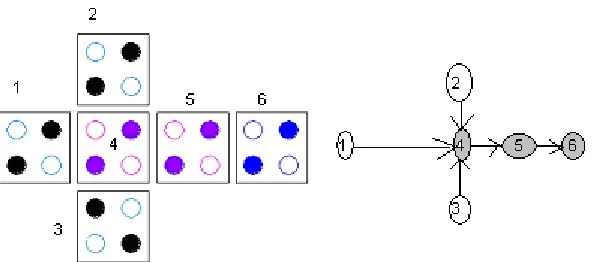
The selection is based on the fitness function defined in equation 2, the individual having highest fitness value has large probability to come to stable condition. and the individual chromosome with lesser probability will be removed. Figure 2 and 3 shows the majority QCA gate, we number a,b and control inputs as 1,2,3 chromosomes and the middle QCA cell is a 4th chromosome and output cells as 5th and 6th chromosome as shown in figure 5 . As per majority logic 4th cell has replicate of one of the inputs, therefore the 4th QCA cell and its interaction with the 5th and 6th cell are considered here. Hence 4th to 6th chromosome must be brought to the perfect ground state condition. For crossover we need not compare the same genes from the first position to third position, we randomly select a hybridization location from the different genes of the two chromosomes as shown in figure 6. The genes in the parent A and B are identical from the first to third bit, thus hybridization location can only random select from the fourth to sixth bit.
Figure 5 Majority QCA gate with 1, 2, 3 input chromosome and 4, 5 and 6 output chromosomes
Figure 6 Crossover Regulation of Majority QCA gate
The outcome of the crossover is shown in figure 5 . For every gene in the population has identical mutation probability. The calculation (simulation) is terminated as soon as iterative generation reaches maximum generation and defined as termination condition. Initially maximum population and temperature is set, then randomly select near by cell or state in the adjacent domain and calculate the probability as in equation 3.
f(xij) = min { 1, exp( (g(i) - gmax) / temp)} (3)
From these again new population is produced. We compute the fitness function decided by fitness values. (Energy values as in [15]) and select maximum value chromosome as the new population, then perform mutation for next population. Termination is achieved when simulation has reached maximum generation condition. The temperature for the simulation considered here is 7K.
4. Simulation results
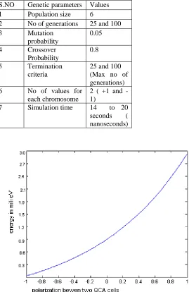
Figure 7 shows the plot of polarization value +1 to -1 with respect to its ground energy, it was proved in [15] the
Hybridization
location
Parent A 1 2 3 4 6 5 offspring A1 1 2 3 4 5 6
the electrons in a QCA cell, for more than 5 generations the polarization reaches perfect +1 or -1 condition. The conditions for simulations are given in table 2.
Table 2 Genetic algorithm parameters for simulation
S.NO Genetic parameters Values
1 Population size 6
2 No of generations 25 and 100 3 Mutation
probability
0.05 4 Crossover
Probability
0.8 5 Termination
criteria
25 and 100 (Max no of generations) 6 No of values for
each chromosome
2 ( +1 and -1)
7 Simulation time 14 to 20 seconds ( nanoseconds)
Figure 7 Plot of polarization of QCA cell with respect to its energy value
Figure 8 Plot of fitness function in terms of polarization and no of generations
Figure 9 Energy value of electron in QCA cell versus no of generations
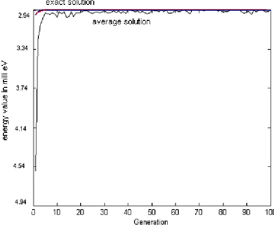
Minimization of function mentioned with the set of values for 100 generations are also simulated, here we have included worst case chromosome (lesser probability) taken along with the best chromosomes. Figure 9 shows the plot of generation versus energy of fitness function for average track of solution and best solution. It is shown that best solution red line falls near to ground state condition of 2.99 milli eV.
Next we have considered the cell to cell response function as non-linearity function i.e. Fitness function; Equation 4 gives non –linear response of QCA cell to its neighboring QCA cell.
F(x) = - tanh (x / 2) (4)
stability for 25 no of generations. Black line shows the average solution of best and worst case chromosome and blue line shows best solution which reaches near to ground state configuration. We have validated our graph with QCAdesigner tool in [16] which shows polarization value between 0 to 0.5 has instability region, by this algorithm we found near to ground state is around 0.58. Whenever polarization reaches between 0.6 to 1.0, QCA cell reaches steady state rotation condition. Next we have considered interaction between two QCA cells (two chromosomes). Figure 11 shows plot of cell to cell response in terms of polarization of two QCA cell. Marked points (circle) on the plot are the instability region. The best value for achieving ground state from our simulation is 0.58 for fixed 25 no of generations. Two different values are substituted in the fitness function and we found the interaction of first QCA cell with the second QCA cell. Figure 12 shows the difference between QCA cell with and without achieving ground state. Black curve corresponding cell has lesser probability and shows instability and red curve stabilizes around 0.6. For unstable QCA cell we have assumed lesser probability which is worst case chromosome, which will never reach ground state condition.
Figure 11 cell to cell (chromosome) response in terms of its polarization.
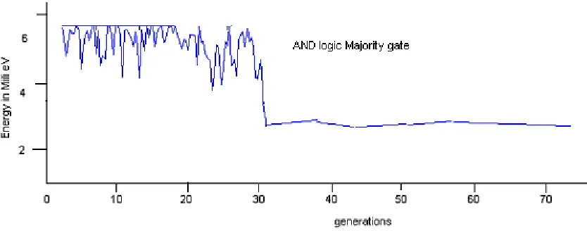
Finally we plot for AND and OR majority gate the ground state achievement of output cell i.e output chromosomes ( 5th and 6th chromosome) as in figure 13 and 14 . We note down that ground state achievement for both the majority gate is around 3 Miili electron volt. We have simulated maximum of 100 generations, stability condition is achieved for about 30 generations for AND gate and 35 generation for OR gate. The probability of achieving ground state by the genetic simulated annealing algorithm is 0.98 ( 2.99 of 3 milli ev) which is higher than the probability of 0.95 simulated from QCAdesigner tool as shown in figure 15.
Figure 13 Plot of Energy versus no of generations of AND gate majority logic
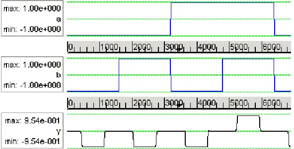
Figure 15 Simulated waveform of QCA AND gate from QCADesigner tool has probability of 0.95
5. Conclusion
We have used genetic simulated annealing algorithm for finding ground state configuration in terms of polarization and energy of elementary logic gates AND and OR QCA circuits. The probability of getting correct polarization by genetic annealing method is 0.98 than other QCA circuit simulation methods using QCAdesigner tool. It was found that the instability in the polarization QCA cell lies between 0 – 0.6 for +1 polarization ( 0 to -1 for -1 polarization) and this can be validated by cell to cell response in QCA circuits. We found the minimum energy or ground state around 3 Milli electron volt for a QCA cell and can be brought to stable condition using Genetic stimulated annealing algorithm. QCA AND and OR gates are simulated for 200 generation and around 40 generations both the circuits are stabilized. This study can be extended to other QCA circuits as well as optimization of number of QCA cells in a QCA circuit.
Reference
[1] K.Walus, Wei Wang and Julliaen et al, “Majority logic reduction for Quantum Cellular Automata” in Proc IEEE Nanotechnology conf, vol 3 December 2004.
[2] K.Walus, Wei Wang and Julliaen et al, “Quantum Cellular Automata adders” in Proc IEEE Nanotechnology conf, vol 3 page461-463December 2004.
[3] K.Walus, Schulaf and Julliaen et al, “High level Exploration of Quantum Dot Automata” in Proc IEEE Nanotechnology conf, vol 2,page 30- 33 2004
[4] K.Walus, Schulaf and Julliaen et al, “Circuit design based on majority gates for application with Quantum dot cellular automata” in Proc IEEE Nanotechnology conf, vol 4,page 1350- 1354, 2004.
[5] K.Walus, Dimitrov and Julliaen et al, “Computer Architecture structure for Quantum Cellular Automata”in Proc IEEE Nanotechnology conf, vol 3,page 1435 – 1439 2003
[6] K.Walus, Dysart and Julliaen et al, “QCQ Designer A Rapid design and simulation tool for quantuim dot cellular automata” in IEEE transactions on Nanotechnology conf, vol 3,No – 2 June 2004.
[7] K.Walus, Dysart and Julliaen et al, “Split current Quantum dot cellular automata modeling and simulation ” in IEEE transactions on Nanotechnology conf, vol 3 March 2004.
[8] A. Vetteth et al., “Quantum dot cellular automata carry-look-ahead adder and barrel shifter,” in Proc. IEEE Emerging Telecommunications Tech-nologies Conf., 2002.
[9] C. Lent and P. Tougaw, “A device architecture for computing with quantum dots,” in Proceeding of the IEEE, vol. 85-4, pp. 541–557, April 1997.
[10] Orlov, R. Kummamuru, R. Ramasubramaniam, C. Lent, G. Bernstein, and G. nider, “Clocked quantum-dot cellular automata shift register,”
Surface Science, vol. 532, pp. 1193–1198, 2003.
[11] C. Lent, B. Isaksen, and M. Lieberman, “Molecular quantum-dot cellular automata,” Journal of American Chemical Society, vol. 125, pp. 1056–1063 -2003.
[12] J. Timler and C. Lent, “Maxwell’s demon and quantum-dot cellular automata,” Journal of Applied Physics, vol. 94, pp. 1050–1060, July 2003.
[13] J.Timler and C.Lent “Quantum Computing with Quantum-dot Cellular Automata using Coherence Vector Formalism “ IEEE nano conference 1998 pp 4361 – 67.
[14] M.Maucci, G.Innaccone, S.Francavigilia and B.Pellegrini “ Semiclassical simulation of Quantum cellular automation circuits” International journal of circuit theory and applications, 2001, Vol – 29, pp 37 – 47.
[15] Sanjukta Bhanja, Marco ottavi, Fabrizia Lombardi, Salvatore Pontarelli “Novel Designs for Thermally Robust Coplanar Crossing in QCA” Proceedings of the conference on Design, automation and test in Europe: ProceedingsMunich, Germany SESSION: Reliability issues for nanotechnology circuits,Pages: 786 – 791, Year of Publication: 2006 ISBN:3-9810801-0-6
![Table 1 – Majority voting scheme [4] [5] INPUT](https://thumb-us.123doks.com/thumbv2/123dok_us/9606286.1489059/2.612.86.230.568.702/table-majority-voting-scheme-input.webp)
![Figure 4 shows clocking scheme of QCA circuits [4][5]](https://thumb-us.123doks.com/thumbv2/123dok_us/9606286.1489059/3.612.71.243.121.276/figure-shows-clocking-scheme-qca-circuits.webp)