MODIFIED SEVEN LEVEL MULTIPLE-POLE PWM
AC–AC CONVERTERS WITH REDUCED
COMPONENTS COUNT
Deepa Nidanakavi
1, J.Lakshmi
2, A.Srilatha
3Associate Professor1 , Assist.Prof 2,3 Department.of Electrical Electronics Engineering
Sphoorhty Engineering College Affiliated to JNTUH, Hyderabad, Telangana (India)
ABSTRACT
The proposed three-phase front-end bidirectional seven-level (7L) rectifier and rear-end 7L inverter are constructed based on multiple-pole multilevel diode-clamped (M2DCC)approach, which consist a total number of 48 diode components clamped. To achieve light weight, efficiency, and better input current quality a novel multilevel ac/dc/ac converters with reduced number of semiconductor devices is proposed in this paper. Higher n-level ac/dc/ac converter topologies offer an alternative solution to address the implications of high-switching-frequency operation. These higher n-level converters have the natural ability to achieve better efficiency with lower switching and conduction losses while operating at lower switching frequency, the number of switching devices can be further reduced based on the M2DCC concept to construct a new unidirectional front-end rectifier (M2SCR).Results obtained show that low current harmonic distortions of 5% and high power factor of 0.99 are achieved with small input inductors despite low-switching-frequency operation at 1 kHz. This seven level multiple pole ac/dc/ac converter is fed to permanent magnet synchronous motor (PMSM)
I INTRODUCTION
In this paper a novel multilevel ac/dc/ac converters with reduced number of semiconductor devices is proposed to achieve light weight, efficiency, and better input current quality Higher n-level (such as 7L) ac/dc/ac converter topologies offer an alternative solution to address the implications of high-switching-frequency operation.
synchronous generator wind turbine with grid connected. To achieve optimum performance simple control techniques can be implemented, due to the advantage of decoupling both front-end source and rear-end load through a dc link.
For higher n-level the realizing dc-link capacitor voltages are the greatest problem output diode-clamped converters. Thus, it results to poorer input and output performance. In between front-end rectifier and rear-end inverter, this unbalanced condition can be solved with the introduction of a multi winding transformer connected to multi pulse diode bridge rectifiers or an additional dc/dc balancing circuit
The future development of multilevel converters involves reducing the overall cost and size needed .An additional dc/dc voltage balancing circuit would be more preferable than implementing a bulky and costly multi winding transformer among the two solutions. For the motor drive applications many classical configurations of high-power transformerless seven -level (7L)ac/dc/ac drive have been experimented . with the proposed power factor correction technique to yield a fair analysis, the performances of both the proposed front-end rectifiers with the 7L-M2DCI are evaluated. The simulation results obtained along with the verified theoretical analysis have proven the feasibility of the proposed topologies for any ac/dc/ac drive applications.
Good overall performance is also achieved while operating at low switching frequency. The 7L ac/dc/ac drives based on the proposed multiple pole multilevel diode-clamped converter (M2DCC) approach presented in this paper drastically reduce the number of power diodes required.
II. OPERATING PRINCIPLES OF 7L AC/DC/AC TOPOLOGIES
Based on the classical MDCC and the proposed M2DCC approaches this section presents the operating principles of three different 7L ac/dc/ac PWM converters. The derivation of the proposed M2DCR and M2SCR topologies are explained here, whereas the proposed M2DCI topology is detailed .
Seven Level Multiple Pole PWM AC-AC Converter
In this paper the work is extended to seven level multiple pole PWM AC-AC converter. For obtaining seven levels output at the inverter side two more switches and two more diodes are added in each pole for every phase at both rectifier side and inverter side of five level multiple pole PWM AC-AC converter. The controlling circuit for five level multiple pole PWM AC-AC converter is extended to control triggering pulses for seven level multiple pole PWM AC-AC convert
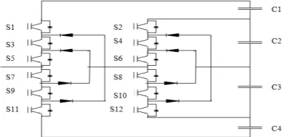
The 7L voltage stepped waveform is obtained with the switching positions based on a single-pole circuit configuration. It can be observed directly that the phase voltage levels are achieved across the point Va to the neutral point m.The classical 7L-MDCC ac/dc/ac converter is a back-to-back (BTB) configuration clamped inverter. In seven level multiple pole diode clamped converter 12 IGBT switches and 8 clamping diodes are used. In overall 72 IGBT switches and 48 clamping diodes utilised. But in classical method 60 clamping diodes are required. So 12 diodes are saved
III PROPOSED SEVEN LEVEL MULTIPLE POLE PWM AC-AC CONVERTER FED TO PMSM.
3.1 Permanent Magnet Synchronous Machine
The permanent-magnet synchronous machine (PMSM) drive has emerged as a top competitor for a full range of motion control applications. For example, in high-power applications the PMSM is widely used in machine tools, robotics, actuators, and is being considered such as vehicular propulsion and industrial drives.
The PMSM is known for having high efficiency, low torque ripple, superior dynamic performance, and high power density. For commercial/residential applications it is also becoming viable. For high-performance applications these drives often are the best choice and are expected to see expanded use as manufacturing costs decrease. In some instances it is referred to as a brushless DC (BDC) machine because by appropriate control it can be made to have input/output characteristics much like a separately excited brush-type DC machine The PMSM is sometimes referred to as a permanent-magnet AC (PMAC) machine or simply as a PM machine.
In the rotorthe use of permanent magnets facilitates efficiency, eliminates the need for slip rings, and eliminates the electrical rotor dynamics that complicate control (particularly vector control). The PMSM also has the drawback of requiring rotor position feedback by either direct means or by a suitable estimation system. The permanent magnets have the drawback of adding significant capital cost to the drive, although the long term cost can be less through improved efficiency
[
𝑉𝑑 𝑉𝑑 𝑉0]
=2 3
[
cos𝜃 cos
(
2𝜋3 -𝜃
)
cos(
2𝜋3 +𝜃
)
sin𝜃 sin
(
2𝜋3 -𝜃
)
sin(
2𝜋3 +𝜃
)
0.5 0.5 0.5
]
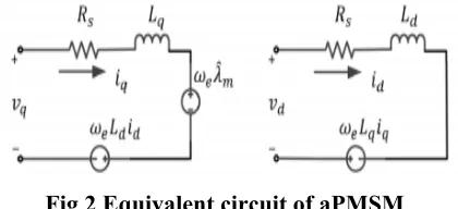
𝑉𝑑=𝑅𝑠𝑖𝑑+ 𝑑𝜆𝑑 𝑑𝑡 -𝜔𝑒𝜆𝑞 (1) 𝑉𝑞=𝑅𝑠𝑖𝑑+ 𝑑𝜆𝑑 𝑑𝑡 +𝜔𝑒𝜆𝑞 𝜆𝑑=𝐿𝑑𝑖𝑑+𝜆𝑝𝑚 𝜆𝑎=𝐿𝑎𝑖𝑎
Where, Ld is the d-axis inductance, Lq is the q-axis inductance, and ܲpm is the amplitude of flux linkage due to the permanent magnet. According to a dynamic equivalent circuit of a PMSM in the d-q frame can be drawn as shown in figure 7.
Fig 2 Equivalent circuit of aPMSM
In the d-q frame, the input power of a PMSM can be written as
(2)
𝑃𝑖𝑛=32
(
𝑉𝑑𝑖𝑑+𝑉𝑞𝑖𝑞)
Assuming the motor losses are negligible, then the input power equals the output power, ܲout of the motor, which can be represented as follows
(3)
𝑃𝑜𝑢𝑡=32𝜔𝑒
(
𝜆𝑝𝑚𝑖𝑞+(
𝐿𝑑-𝐿𝑞)
𝑖𝑑𝑖𝑞)
Since the output power is a product of the motor mechanical speed time the developed/output torque, the output torque can be obtained as:
(4) 𝑇𝑒= 𝑝𝑜𝑢𝑡 𝜔𝑚 = 𝑝 2 3
2
(
𝜆𝑝𝑚𝑖𝑞+(
𝐿𝑑-𝐿𝑞)
𝑖𝑑𝑖𝑞)
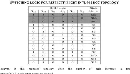
TABLE I
SWITCHING LOGIC FOR RESPECTIVE IGBT IN 7L-M 2 DCC TOPOLOGY
However, in this proposed topology when the number of cells increases, a total number of 6(n-3) diode components are reduced.
Based on the multiple pole hierarchy the 7L voltage stepped waveform of the M2DCC topology is achieved with the switching positions.
3.2 Proposed Unidirectional Front-End 7L M2SCR WithRear-End 7L-M2DCI Topology
To achieve 7L input voltage stepped waveform each phase leg of the proposed unidirectional 7L-M2SCR also requires two cells, as shown. For certain ac/dc/ac drive applicationsa bidirectional power flow in the front-end rectifier is not required such as propulsion, compressor, or any non regenerative braking system. Thus, a proposed transformerless front-end unidirectional rectifier is reconstructed in Fig. 3 with the arrangement of the semiconductor devices in the bidirectional M2DCR configuration
f o l low s
For the outer cell and similarly for the inner cell the states selection of the top and bottom diodes of a M2SCR is dependent on 1-Sa1 and 1-Sa2. Hence, only two switching devices are required in each cell, with four series diodes connected to the terminals of the capacitors in the dc link. Due to lesser number of switches needed, higher power efficiency is achieved with lesser switching and conduction losses. To the neutral-point clamped of the four dc-link capacitors the two switching devices (Sa3 and Sa4) of the inner cell are connected directly, whereas the other two switching devices (Sa1 and Sa2) of the outer cell are clamped to the output terminals of the inner cell..
3.3 General Characteristic of the Classical and Proposed7L AC/DC/AC Converters
The proposed 7L ac/DC/AC converters of general characteristics of the classical is explained. The front-end rectifier and the rear-end inverter of 7L ac/dc/ ac drives are operated independently with same level-shifted PWM (LS-PWM). To achieve the desired switching signals the LS-PWM requires a reference signal and a set of four 1-kHz triangular carriers for the respective semiconductor switches. The switching function of the LS-PWM technique for the7L rectifiers and inverters is expressed as
{
𝑆𝑎1(𝑡) =𝑇𝑎1(𝑡) = 2𝑚𝑎sin𝜔𝑡-1𝑆𝑎2(𝑡) =𝑇𝑎2(𝑡) = 2𝑚𝑎sin𝜔𝑡
(5)
{
𝑆𝑎3(𝑡) =𝑇𝑎3(𝑡) = 2𝑚𝑎sin𝜔𝑡+ 1𝑆𝑎4(𝑡) =𝑇𝑎4(𝑡) = 2𝑚𝑎sin𝜔𝑡+ 2
wherema is the ratio of two times the fundamental component of pole voltage to the dc-link voltage.
Fig.4. Ripple current versus modulation ratio of rectifier
Under the condition of steady state and balanced dc-link voltage, the general incremental output pole voltage equation is expressed as
(6)
Vxm(t) =Vndc‒(t)1
(
∑i = 1n‒1Txi-n‒21)
(7)
{
𝑀𝑥,𝑟𝑒𝑐𝑡𝑖𝑓𝑖𝑒𝑟(𝑡) =𝑉𝑑𝑐(𝑡)
𝑉𝐿-𝐿(𝑡), 𝑀𝑥,𝑟𝑒𝑐𝑡𝑖𝑓𝑖𝑒𝑟(𝑡) > 1
𝑀𝑥,𝑟𝑒𝑐𝑡𝑖𝑓𝑖𝑒𝑟(𝑡) =2𝑉𝑉𝑥𝑚(𝑡)
𝑑𝑐(𝑡), 𝑀𝑥,𝑟𝑒𝑐𝑡𝑖𝑓𝑖𝑒𝑟(𝑡)≤1
whereVxm(t) is the output pole voltage referred to the inverter side . Vx, L−L(t) is the line-to-line grid voltage.
IV. HIGH-POWER-FACTOR OPERATION OF THREE-PHASE 7L M 2DCR AND M2SCR RECTIFIERS
A. Semiconductors Voltage and Current Stresses
For the respective front-end rectifiers are derived with the switching function in (1) and based on the the voltage and current stress expressions following
The voltage and current stress expressions for the respective front-end rectifiers are derived with the switching function in (1) and based on the following In the converter design voltage and current stresses are the dominant factors considered, so that the converter can achieve optimum performance with higher reliability. For the proposed front-end rectifiers Proper selection of device rating is determined based on the global stress analysis. The maximum voltages across the power devices of unidirectional 7L-M2SCR and bidirectional 7L-M2DCR are respectively expressed in the following:
(8)
{
VDa1=3Vdc 4
VDa4= Vsa1=3V8dc VDa2= VDa3= Vsa2=
Vdc 4
(9)
{
VSa1=3Vdc 4
VSa4=3V8dc VSa2= VSa3= VDa1= VDa2=
Vdc 4
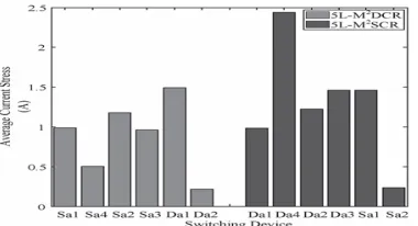
For the power devices in the upper phase leg, Since the maximum voltage stress expressionsare (9) and (10).Using the same expressions the respective complimentary power devices in the lower phase leg are also determined. Based on the assumed five factors (1)–(5) the average current stress is analyzed over one period of the fundamental frequency For simplification, the average current stress is approximated as follows based on respective switching functions
𝐼𝑠𝑎(𝑜𝑢𝑡𝑒𝑟𝑐𝑒𝑙𝑙)(𝑡) =𝐼𝐷𝑎(𝑜𝑢𝑡𝑒𝑟𝑐𝑒𝑙𝑙)(𝑡) = 1 2𝜋
∫
2𝜋
0
𝐼𝑎sin (𝜔𝑡)𝑆𝑎(𝑜𝑢𝑡𝑒𝑟𝑐𝑒𝑙𝑙)𝑑𝜔𝑡
(10)
𝐼𝑆𝑎(𝑖𝑛𝑛𝑒𝑟𝑐𝑒𝑙𝑙)(𝑡) =𝐼𝐷𝑎(𝑖𝑛𝑛𝑒𝑟𝑐𝑒𝑙𝑙)(𝑡) =21𝜋∫2𝜋
0 𝐼𝑎sin𝜔𝑡*
[
2 -4𝑉𝑎𝑚(1)𝑉𝑑𝑐 sin𝜔𝑡
]
𝑆𝑎(𝑖𝑛𝑛𝑒𝑟𝑐𝑒𝑙𝑙)𝑑𝜔𝑡diodes during the positive cycle conduction period. Hence, the final net average current stress of the 7L-M2DCR in Fig. 8 is found much lower compared with that of the 7L-M2SCR.
B. Input Current Shaping of the 7L-M2DCR andthe 7L-M2SCR
The reverse current through the semiconductor switches in the bidirectional 7L-M2DCR will be cancelled out. In the upper phase leg of the proposed front-end rectifiers final average current stress for the respective power devices are shown in Fig. 8.
Fig.5. Average current stress level for each devices of the respective front-end rectifier topologies. as 1.
In this case the current harmonic distortion can be minimized by increasing the switching frequency to 5 kHz and higher.when the voltage transfer ratio Mx, rectifier is greater than 1.3. This can be proved by substituting (6) into (4), where fsis observed to be cancelled away. However, the grid current distortion does not deviate much with any range of switching frequency utilized.
C. Control Theory
For the respective semiconductor switches the LS-PWM requires a reference signal and a set of six 1- kHz triangular carriers to achieve desired switching signals. The front-end rectifier and the rear-end inverter of seven level of 7L ac/dc/ac converter are operated independently with same Level- shifted PWM (LS-PWM). Under the condition of steady state and balanced dc-link voltage, the general incremental output pole voltage equation is expressed as
(11)
𝑉𝑥𝑚(𝑡) =
𝑉𝑑𝑐(𝑡) 𝑛-1
(
∑𝑛-1 𝑖= 1𝑇𝑥𝑖
-𝑛-1
2
)
Where, ‘x’ represents phase “a,” “b,” and “c;” and n is the number of voltage level. High modulation index of the front-end rectifier is required to mitigate the input current distortion and achieve good voltage tracking due to its boosting effect in nature. Meanwhile, the rear-end inverter must be operated at the linear region.
current with constant unity power factor SRF controller provides a good dynamic response performance and
overall efficiency, and lightest weight among the other rectifier topologies.
D. Unbalanced DC-Link Capacitor Voltages
If the power converter is not adequately designed, the unbalanced dc-link capacitor voltages may disrupt the smooth operating system and affect the global reliability. By overstressing the limited blocking voltage capability of the semiconductor devices this disastrous condition will damage the converter. When any fault condition occurs by disabling the rectifier/inverter operation although this undesirable condition can be typically resolved, the overall efficiency of the system may be greatly affected.
To ensure that the power device ratings are properly selected the alternative solution to overcome this issue is during the design ,according to the worst case scenarios. Thus, the maximum voltage stress across the respective power devices of the 7L rectifiers. The obtained results are co simulated between PSIM and MATLAB Simcouple. As a result, for the classical 7L rectifiers it is essential to have series-connected switches, but these additional switching devices can be avoided for the proposed 7L topologies.It should be noted in the proposed 7L rectifiers under unbalanced condition is Vdc, that the maximum voltage stress across the semiconductor switches, unlike in the classical 7L rectifiers, which will be experiencing 2Vdc (twice the dc-link voltage).
E. SRF Current Control Scheme
The proposed control algorithm with power factor correction technique is shown,to regulate the dc-link voltage and mitigate the current distortions. two control loops, i.e., synchronous-reference-frame (SRF) current control and constant switching frequency modulation, are implemented
The detailed analyses of the outer-loop dc-link voltage control and the inner-loop current control are both presented. For the dc–dc balancing circuit the balancing control is presented in [12] and [13].Due to the simplicity of the control strategy, low-cost integrated control circuit can be designed. The unity power factor controller for the front-end 5L rectifiers ( M2DCR or M2SCR) designed is based on the SRF current control with the LS-PWM technique.
To achieve high quality input sinusoidal current with constant unity power factor performance SRF controller provides a good dynamic response. Under steady-state condition the open-loop transfer function of the dc-link voltage control is written as follows to achieve a stable control system:
(12) 𝐿(𝑠) = 𝐾𝑝𝑠+𝐾𝐼 𝑠 . 𝐿𝑥𝐼𝑑 𝐶𝑒𝑞𝑉𝑑𝑐.
(
3𝑉 𝑝 𝐿 𝑥𝐼𝑑 -𝑠)
𝑠+(
𝐼 𝑑𝑐 𝐶 𝑒𝑞𝑉𝑑𝑐)
and the input (phases a, b, and c) filter inductance with the values of 600 μF and 5 mH, respectively. Kp and KI are the proportional and integral parameters of the dc voltage control loop selected at 0.4 and 15, respectively. Vp is the RMS value of the grid phase voltage, and Vdc is the mean value of the dc link voltage. The feed forward current control loop under steady-state condition is derived based on the power balanced principle, which is expressed in the following:
(13)
𝐾𝑓= 𝑉3𝑑𝑐
𝑉𝑝
whereVpis the RMS value of the grid phase voltage.
V. SIMULATION RESULTS
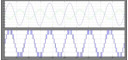
The operation of the proposed bidirectional 7L-M 2DCR has been evaluated with the power factor control under various load conditions. Figs. 9 and 10 show the unity power factor operation under two different types of loading effect. However, the proposed unidirectional 7L-M 2 SCR topology can only achieve unity power factor without any reversal power capability with same performance obtained in Fig. 9
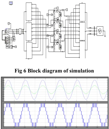
Fig 6 Block diagram of simulation
Fig. 8. Unity power factor operation with inverting mode. (a) Voltage and current at the grid side. (b) Pole voltage at the rectifier side.
Fig. 9. Leading power factor, PF = 0 .43. (a) Voltage and current at the grid side. (b) Pole voltage at the rectifierside..
Fig. 10. Lagging power factor, PF=0.43. (a) Voltage and current at the grid side. (b) Pole voltage at the rectifier side.
TABLE II
VI. CONCLUSION
In seven level multiple pole PWM AC-AC diode clamped converter Permanent Magnet Synchronous Motor is connected at output side of inverter. PMSM rotates with synchronous speed in both inverting and rectifying modes the speed and torque variations are observed. But the PMSM acts as motor in inverting mode and acts as generator in rectifying mode. To reduce the number of semiconductor devices compared with the conventional converters a new generation of front-end bidirectional 7L-M 2DCR topologies has been introduced in this paper. With low operational switching frequency of 1 kHz without the aid of any bulky LC passive filter excellent performance and low input current distortion with high power factor is achieved. In addition to that, the reduction of component counts allows the proposed converters to achieve low voltage/current stress and low switching losses.However, the dc-link voltage balancing circuit is restricted to certain power applications. These will provide a more cost-effective and energy-efficient solution for a higher level ac/dc/ac drive and can particularly be suitable for renewable energy conversion where high efficiency is paramount. By using simulation results we can analyze the overall converter efficiency is also improved. The size of input reactors is greatly reduced as well because of the incremental voltage stepped waveforms synthesized at low switching frequency. In the dc link this is at the small cost of having an additional voltage balancing circuitry to balance the capacitor voltages.
REFERENCES
[1] K. A. Corzine and J. R. Baker, “Reduced-parts-count multilevel rectifiers,” IEEE Trans. I nd. Electron., vol. 49, no. 4, pp. 766–774,Aug. 2002.
[2] J. K. Steinke, “Use of an LC filter to achieve a motor-friendly performance of the PWM voltage source inverter,” IEEE Trans. Energ y C onvers.,vol. 14, no. 3, pp. 649–654, Sep. 1999.
[3] A. I. Maswood, O. H. P. Gabriel, and M. A. Rahman, “High power multilevel inverter with unity PF front-end rectifier,” in Proc. IEEE ITE, 2012, pp. 1–5.
[4] A. I. Maswood, O. H. P. Gabriel, and E. Al Ammar, “Comparative study of multilevel inverters under unbalanced voltage in a single dc link,” IETPower Electron., vol. 6, no. 8, pp. 1530–1543, Sep. 2013.
[5] A. I. Maswood and L. Fangrui, “A unity power factor front-end rectifier with hysteresis current control,” IEEE Trans. Energy Convers., vol. 21, no. 1, pp. 69–76, Mar. 2006.
[6] C. Kuei-Hsiang, C. Pi-Yun, and C. Chun-Hsin, “A three-level converter with output voltage control for high-speed railway tractions,” in Proc.33rd Annu. IEEE IECON, 2007, pp. 1793–1798. [7] J. Yang, F. C. Lee, and L. Sizhao, “Space vector modulation for threelevel NPC converter with neutral point voltage balance and switching loss reduction,” IEEE Trans. Power Electron., vol. 29, no. 10, pp. 5579–5591, Oct. 2014.
[9] S. Jie, S. Schroder, B. Duro, and R. Roesner, “A neutral-point balancing controller for a three-level inverter with full power-factor range and low distortion,” IEEE Trans. Ind. Appl., vol. 49, no. 1, pp. 138–148,Jan./Feb. 2013. [10] A. I. Maswood and L. Fangrui, “A novel unity power factor input stage for ac drive application,” IEEE Trans.
Power Electron., vol. 20, no. 4, pp. 839–846, Jul. 2005. [11] J. Minibock and J. W. Ko lar, “Novel concept f or multilevel inverter.
DEEPA NIDANAKAVI
Completed B.Tech in Electrical &Electronics Engineering in 2006 from JNTUH, Hyderabad and M.Tech in Power Electronics in 2009 from G. Narayanamma Engineering College Affiliated to JNTUH, Hyderabad. Working as Associate Professor at SphoorthyEnggineering ,Nadergul, Hyderabad, Telangana, India. Area of interest includesPower Electronics,power systems, electrical drives control.
J.LAKSHMI
Completed B.Tech in Electrical &Electronics Engineering from JNTUH, Hyderabad and MEAffiliated to OU, Hyderabad. Working as Assistant Professor at SphoorthyEnggineering ,Nadergul, Hyderabad, Telangana, India. Area of interest includesPower Electronics,power systems, electrical drives control.
SRILATHA.ANNREDDY