A study of Bs2 chip for personal computer
controlled six power transistor inverter for
three phase induction motor speed control
(1) M.C. OKENWA
Department of Electrical Engineering of Nnamdi Azikiwe University, Awka,Nigeria. Email:[email protected], [email protected]
Phone: +2348022600700, +2349092441770
(2) EZECHUKWU O.A
Department of Electrical Engineering of Nnamdi Azikiwe University, Awka,Nigeria.
(3) UMUNNA C.O
Department of Electrical Engineering Of Nnamdi Azikiwe University, Awka, Nigeria
Abstract
A Bs2 chip to produce six sequential pulses for Pc controlled transistorized inverter was designed and implemented. It has electrically erasable device (EEPROM) and facility for pulse width modulation. The development involved design of Bs2 software program fed to transistorized inverter. 0.3KW transistorized inverter is triggered sequentially which was used to drive 250watt induction machine to full speed of 1800rpm.
Keyword: Bs2chip; bipolar transistor switch; induction motor speed control; six sequential pulses; PBasic instructions
1. Introduction
Variable speed drives are today increasingly being applied in many industrial control systems. In the past, D.C motors were used in areas where variable speed operation was required because their flux and torque can be controlled by two independent orthogonal Variables; stator current and rotor flux. Consequently, they require periodic maintenance. They cannot be used in an explosive environment because of sparking due to brush and commutation action. These problems can be avoided by the application of induction motors. Induction machines have simple and rugged structure, high maintainability and economic considerations. However, the speed or torque control of the new control system for induction motors include: variable voltage, variable frequency, inverse-parallel thyristor, auto-transformer tap changing, pulse width modulation (PWM) and flux vector control. These make it possible to vary the speed and torque of an induction machine in a manner similar to that of a separately excited DC motor.
In this study, BS2 chip is used to trigger 0.3KW transistorized inverter to control the speed of 250watt induction machine. This induction motor control is only used for the prototype design presented in this work. A 230VDC bus line is modulated with pulse width modulation (PWM) inherent in BS2 chip. This provides the variable speed output. This also upholds a constant voltage to frequency ratio for constant torque throughout the speed range. BS2 chip pulses have a dead time of 50 micro seconds (1/200) which disallowed the short circuiting of two parallel BJT transistors (TI and T4 IN Fig 4). The six power transistor inverter is switched sequentially by firing pulses produced by BS2 microprocessor chip. The preponderance of discrete Components to produce triggering pulses for transistor inverter switching declined tremendously with the advent of the microprocessor. The microprocessor produces pulses, and then fed to switching devices via its input/output point which are properly ritualized in the computer programme. Moreover, the power transistor inverter could be power bipolar transistor (BJT), power metal oxide semiconductor field effect transistor (MOSFET) or insulated gate bipolar transistor (IGBT) switched in six steps to synthesis the three phase output fed to induction machine. The power BJTS are used for 250watts induction motor. The power BJT inverter must switch fastly to produce PWM output.
Interestingly, the incessant demand for microprocessor induction motor control system has justified the need for this work.
2. Background
2.1 transistor switch
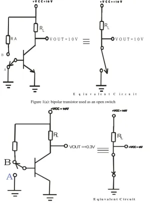
saturation conditions. Figure 1(a) depicts the base shorted to ground. With no forward bias on the base emitter junction, there is no voltage to develop a base current. The result is that the transistor is cut off and there is no connection between the collector and emitter. It can be determined whether the transistor is not conducting by measuring the voltage from collector to the ground. The reading should show a value equal to the supply voltage. An open switch will also have the full voltage present across its terminals in the equivalent circuit. Figure 1(b) shows the base-emitter junction forward biased when the base is connected to RA. If the resulting base current is large enough, the collector current will reach its maximum, or saturation value. In this condition a short circuit between the collector and emitter occur. A value above zero volts from collector to ground indicates that the transistor is fully on. A closed switch in the equivalent circuit will have zero volt present across its terminals.
A
+ V C C = 1 0 V + V C C + = 1 0 V
RL RL
R A V O U T = 1 0 V V O U T = 1 0 V
B
E q i u v a l e n t C i r c u i t Figure 1(a): bipolar transistor used as an open switch
+VCC = 10V
RL
+VCC = 10V
+VCC = 0V
E q i u v a l e n t C i r c u i t VOUT =+0.3V
B
A
RL
Figure 1 (b): Bipolar transistor used as a closed switch
In this work 0.3KW transistorized inverter is used to control 0.25KW Induction motor. The switching circuit encompasses six power Bipolar transistors. Thus, the load is 250W. We are to design a 0.3kW three phase BJT inverter to drive the load (250W).
Basically, power = voltage x current (1)
Known parameters: power = 300W
Voltage = 230V dc bus Therefore; current = 300/230=1.304A
So, the BJT (bipolar transistors) not less than 400v and 2A are selected.
the transistor to saturate. A zero volt input will drive the transistor into the cut off condition. Resistor Rb limits the base current to a safe value. Resistor Rc represents the load such as a relay coil or induction machine.
R b
+VCC
R c
Computer Microprocessor
5 v
Figure 2: a transistor switched on or off by a microprocessor
2.2 BS2 Chip firing pattern for six BJT power transistor inverter
The use of BS2 Chip to produce triggering pulses supersedes that of discrete component because of its numerous advantages. These include smaller physical size then occupies small space, reliability, flexibility, high clocking frequency, has electrically erasable memory device and has facility for PWM. It is user friendly. BS2 chip is power with regulated 9volt supply and has built-in 20MHz oscillator.
Consequently, the BS2 chip commands the operation of the transistor inverter by the use of software design. This chip understands PBASIC (programming Basic) or other higher level language. In this work, PBasic has been used. The PBASIC instructions include: pause, Goto, delay, CON, high, Low, rotate, reverse, return, if-then, if-then/else, for-next etc. These instructions when applied give linear coding, branching, loops and subroutine.
The BS2 chip produces six sequential square wave pulses for the firing of the six BJT inverter. The pulses have variable delay time of 1/200s. This dead time prevent short circuiting of two parallel transistors. A personal computer is used to accelerate or decelerate the on-time.
Bs2 CHIP
R P1
P 2
P3 P4
P 5
P6 +VCC=5V
LED
R R R R R
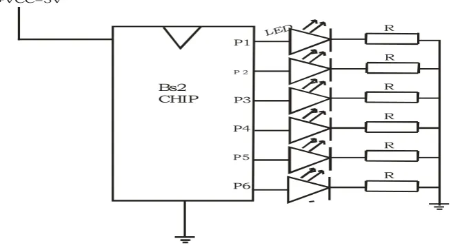
Figure3: The BS2 chip firing Circuit
In Fig.3, each LED must have a resistor connected in series to limit the forward current. This forward current may be maximum value of 0.01A. This forward current causes a 2vdrop across the LED. The value of the series resistor to use can be calculated from the expression below.
2.3 The transistor Inverter Switching Model
+V
T1 T3 T4
T5 T6 T2 C OV
B A
AC
Th ree Ph ase M ot or
Figure 4: Transistor Inverter Switch Model
From fig.4, three switches A,B and C are connected in parallel across a DC supply. The switch positions connect either positive voltage or ground to the swivel terminal. The voltage is positive in the up position and zero in the down position.
The transistors (T1,T4,T3,T6,T5,T2) in the transistor inverter perform the switching. The swivel terminal ‘A’ represents the junction between transistor T1 andT4. The swivel terminal ‘B’ represents the junction between T3 and T6. Also, the swivel terminal “C” represents the junction T5 and T2. Where all six switching transistors are sequenced properly, they develop square wave signals to simulate three phase voltage patterns.
3 Ac Drive Speed control Model
The speed is reciprocal of the period in seconds. Speed is also determined by the number of Poles. The speed of a given Ac induction motor is derived from the following equation.
N = 60f/P (3)
F = 1/T (4)
Where,
N = Speed (RPM)
f = Frequency (Hz)
P = Number of pole Pairs
60 = To determine RPM, the frequency given in seconds is converted to the number of cycles in a minute by multiplying 60 times f
T = period
3.1 The derivation of a corresponding Revolution per minute produce from BS2 chip.
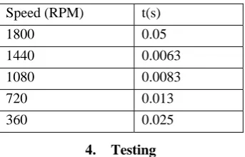
The prototype induction machine has the following specifications: 1800rpm, 250watt. BS2 chip has a variable delay time at 1/200s the induction motor drives at full speed of 1800rpm.
Table1: Speed Driven With Time
Speed (RPM) t(s)
1800 0.05 1440 0.0063 1080 0.0083 720 0.013 360 0.025
4. Testing
The test were performed using PC (personal computer) interface to programmed BS2 chip connected to six bipolar transistor inverter fed to 250watts induction motor.
The 1/200 delay drives 250W induction motor to 1800rpm. The Bs2 chip computer program is shown below
‘Chip type: Basic stamp2 ‘Clocking Frequency: 20MHz
Pin1 CON1
Pin2 CON2
Pin3 CON3
Pin4 CON4
Pin5 CON5
Pin6 CON6
Delay time VAR Byte Step 1:
High pin1 Low pin2 Low pin3 Low pin4 High pin5 High pin6
PAUSE Delay Time GOTO Step2 Step2: High pin1 High pin2 Low pin3 Low pin4 Low pin5 High pin6
PAUSE Delay Time GOTO Step 3 Step 3: High pin1 High pin2 High pin3 Low pin4 Low pin5 Low pin6
PAUSE Delay Time GOTO STEP4 Step 4: Low pin1 High pin2 High pin3 High pin4 Low pin5 Low pin6
Low pin 1 Low pin2 High pin3 High pin 4 High pin5 Low pin6 Pause delay time Goto step6 STEP 6: Low pin1 Low pin2 Low pin3 High pin4 High pin5 High pin6 Pause Delay time Goto Step 1
5. Results and Discussion
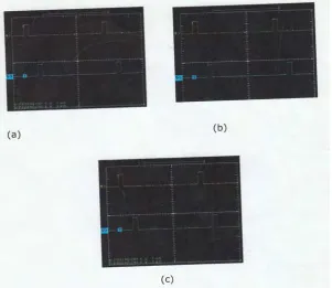
When the BS2 was demonstrated the following wave form were produce
Figure 5: The six sequential waveforms observed on the scope:
a) For transistor T1 and T4 b) For transistor T3 and T6 c) For transistor T5 and T2
As seen from fig.5, and the computer program, they follow six sequential steps.
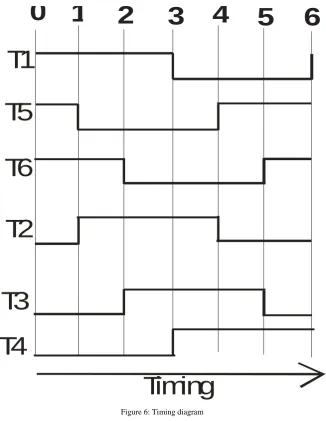
From table I, at a variable delay time, the speed of the induction motor was varied using computer. See fig6 for timing diagram.
0
1
2
3
4
5
6
T1
T5
T6
T2
T3
T4
Timing
Figure 6: Timing diagram
6. Conclusions and recommendation
The BS2 Chip based 0.3kw BJT transistor inverter was developed for 250watts induction motor. The BS2 Chip firing sequence has proven successful. The work has replaced the use of discrete component to produce the pulses. For further work, IGBT transistor inverter is recommended for higher power induction machine.
References
[1] 1 L.M. Terry Barlelt. Industrial control electronics Delmar, a division of Thomson Learning, New York 1997 PP 33-36,191-200. [2] 2 Parallax version 2.0,2014. A Basic stamp syntax and reference Manual. WWW.parallax. Com
[3] 3 S. Vedam. Electrical Drives concepts and Application Mc Graw-Hill publishing company LTD, New York 1996. [4] M.C. Okenwa. Electromechanical devices and machine Unpublished Lecture note. Nnamdi Azikiwe University, Awka 2012. [5] M. Predko. Handbook of Microcontrollers.Mc GRAW-HILL, New-York 1998 PP 771-781.
[6] C.W. Lander. Power Electronics, Mc Graw-Hill Book company England 1987 PP 195- 201.
[7] L. Jones. Basic Electronics. Cambridge University Press, Great Britain 1996 PP 159-164.